EP0688067A2 - Winkelverbinder für Leiterplatten - Google Patents
Winkelverbinder für Leiterplatten Download PDFInfo
- Publication number
- EP0688067A2 EP0688067A2 EP95109385A EP95109385A EP0688067A2 EP 0688067 A2 EP0688067 A2 EP 0688067A2 EP 95109385 A EP95109385 A EP 95109385A EP 95109385 A EP95109385 A EP 95109385A EP 0688067 A2 EP0688067 A2 EP 0688067A2
- Authority
- EP
- European Patent Office
- Prior art keywords
- connector
- housing
- section
- card edge
- printed circuit
- Prior art date
- Legal status (The legal status is an assumption and is not a legal conclusion. Google has not performed a legal analysis and makes no representation as to the accuracy of the status listed.)
- Granted
Links
- 230000006870 function Effects 0.000 description 8
- 229910000679 solder Inorganic materials 0.000 description 7
- 238000003780 insertion Methods 0.000 description 5
- 230000037431 insertion Effects 0.000 description 5
- 239000000463 material Substances 0.000 description 4
- 239000003381 stabilizer Substances 0.000 description 3
- 239000004020 conductor Substances 0.000 description 2
- 238000001816 cooling Methods 0.000 description 2
- 239000003989 dielectric material Substances 0.000 description 2
- 230000009977 dual effect Effects 0.000 description 2
- 238000012986 modification Methods 0.000 description 2
- 230000004048 modification Effects 0.000 description 2
- 239000004033 plastic Substances 0.000 description 2
- 239000002861 polymer material Substances 0.000 description 2
- 230000007797 corrosion Effects 0.000 description 1
- 238000005260 corrosion Methods 0.000 description 1
- 230000007423 decrease Effects 0.000 description 1
- 239000002991 molded plastic Substances 0.000 description 1
- 229920000642 polymer Polymers 0.000 description 1
- 230000000284 resting effect Effects 0.000 description 1
- 230000000717 retained effect Effects 0.000 description 1
- 230000007704 transition Effects 0.000 description 1
Images


Classifications
-
- H—ELECTRICITY
- H01—ELECTRIC ELEMENTS
- H01R—ELECTRICALLY-CONDUCTIVE CONNECTIONS; STRUCTURAL ASSOCIATIONS OF A PLURALITY OF MUTUALLY-INSULATED ELECTRICAL CONNECTING ELEMENTS; COUPLING DEVICES; CURRENT COLLECTORS
- H01R12/00—Structural associations of a plurality of mutually-insulated electrical connecting elements, specially adapted for printed circuits, e.g. printed circuit boards [PCB], flat or ribbon cables, or like generally planar structures, e.g. terminal strips, terminal blocks; Coupling devices specially adapted for printed circuits, flat or ribbon cables, or like generally planar structures; Terminals specially adapted for contact with, or insertion into, printed circuits, flat or ribbon cables, or like generally planar structures
- H01R12/70—Coupling devices
- H01R12/7005—Guiding, mounting, polarizing or locking means; Extractors
-
- H—ELECTRICITY
- H01—ELECTRIC ELEMENTS
- H01R—ELECTRICALLY-CONDUCTIVE CONNECTIONS; STRUCTURAL ASSOCIATIONS OF A PLURALITY OF MUTUALLY-INSULATED ELECTRICAL CONNECTING ELEMENTS; COUPLING DEVICES; CURRENT COLLECTORS
- H01R12/00—Structural associations of a plurality of mutually-insulated electrical connecting elements, specially adapted for printed circuits, e.g. printed circuit boards [PCB], flat or ribbon cables, or like generally planar structures, e.g. terminal strips, terminal blocks; Coupling devices specially adapted for printed circuits, flat or ribbon cables, or like generally planar structures; Terminals specially adapted for contact with, or insertion into, printed circuits, flat or ribbon cables, or like generally planar structures
- H01R12/70—Coupling devices
- H01R12/71—Coupling devices for rigid printing circuits or like structures
- H01R12/712—Coupling devices for rigid printing circuits or like structures co-operating with the surface of the printed circuit or with a coupling device exclusively provided on the surface of the printed circuit
- H01R12/716—Coupling device provided on the PCB
Definitions
- the present invention relates to electrical connectors and, more particularly, to an angled card edge connector.
- U.S. Patent 4,756,694 discloses a dual row connector for receiving memory modules for a low profile package. The connector can receive the memory modules at an angle of 25°.
- U.S. Patents 4,473,263 and 4,862,400 also relate to angled connection of daughter boards to a mother board.
- U.S. Patent 4,241,966 discloses an electrical connector with an ejector-retainer. Other relevant U.S. Patent that disclose ejectors include 5,167,517; 4,898,540; 5,074,800; 4,070,081; 4,579,408; 3,767,974; 4,973,255; 4,975,073.
- a card edge connector comprising a housing and electrical contacts.
- the housing has a first member and a second member.
- the first member comprises a middle section with a card edge receiving area and two rows of contact receiving channels, one at each side of the receiving area.
- the first member also comprises two guiding projections located at opposite ends of the middle section.
- the second member comprises a keeper section with at least four rows of contact passages.
- the housing is suitably sized and shaped to be connected to a mother printed circuit board and have a daughter printed circuit board connected to the housing in the card edge receiving area at an angle of between about 20° and 60° relative to a plane of the mother printed circuit board.
- the electrical contacts are located in the contact receiving channels and extend through the contact passages of the keeper section.
- a card edge connector comprising a housing, electrical contacts, and ejectors.
- the housing has a middle section and two guiding projections located at opposite ends of the middles section.
- the middle section has a card edge receiving area and two rows of contact receiving channels on opposite sides of the receiving area.
- the housing is suitably sized and shaped to be connected to a mother printed circuit board and have a daughter printed circuit board connected to the housing in the card edge receiving area at an angle of between about 20° and 60° relative to a plane of the mother printed circuit board.
- the electrical contacts are located in the contact receiving channels and extend from a bottom of the housing.
- the ejectors are pivotably connected to the housing at the guide projections and are adapted to eject, at least partially, a daughter printed circuit board from the card edge receiving area.
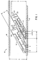
- FIG. 1 there is shown a partial schematic sectional view of an electronic component 10 having electrical connectors 12 incorporating features of the present invention.
- an electronic component 10 having electrical connectors 12 incorporating features of the present invention.
- the present invention will be described with reference to the embodiments shown in the drawings, it should be understood that the present invention can be embodied in various different forms of alternate embodiments. In addition, any suitable size, shape, or type of elements or materials could be used.
- the electronic component 10 includes two parallel mother printed circuit boards 14, 16, two daughter printed circuit boards 18, 20, and two of the electrical connectors 12.
- the two connectors 12 are connected to the first mother printed circuit board 14 and, connect the two daughter printed circuit boards 18, 20 to the first mother printed circuit board 14.
- the electronic component 10 could have only one mother printed circuit board or more than two mother printed circuit boards.
- any suitable number of the connectors 12 could be provided including one or more than two and, could be connected to both of the mother printed circuit boards 14, 16.
- the electronic component 10 could be any suitable type of electronic component, such as a computer.
- the daughter boards 18, 20 are removably connected to the connectors 12.
- the electronic component 10 can be sold without the daughter boards 18, 20 and the purchaser has the option to add the daughter boards to the component at a later date.
- the daughter boards 18, 20 are double sided SIMM printed circuit boards or memory boards.
- any suitable type of daughter boards could be used.
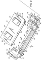
- one of the connectors 12 is shown in a partially exploded view with the first daughter board 18 and ejectors 22.
- the daughter board 18 has contact pads 24 at a card edge 26 and electronics 28 on both the top side 30 and bottom side 32 of the board 18.
- the connector 12 is generally comprised of a housing 34, electrical contacts 36, and the two ejectors 22.
- the housing 34 is comprised of a first member 38 and a second member 40 that are connected to each other. In alternate embodiments one member or more than two members could be used to form the housing 34.
- the two members 38, 40 are both made of dielectric material, such as molded plastic or polymer material.
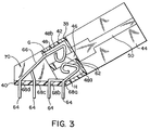
- the first member 38 has a middle section 42 and two guide projections 44 extending out in front of the middle section from opposite ends. Referring also to Fig. 3, the middle section 42 includes a card edge receiving area or slot 46 and two rows of contact receiving channels 48 located on opposite sides of the receiving area 46. The channels 48 intersect with the receiving area 46 and have apertures at the rear of the middle section 42.
- the receiving area 46 is suitably sized and shaped to receive the card edge 26 therein.
- the guide projections 44 have interior facing slots 50 for slidingly receiving end edges 52 of the daughter board 18.
- the guide projections 44 also have exterior facing slots 54.
- the ejectors 22 are pivotably mounted to the guide projections 44 in the exterior facing slots 54.
- the exterior facing slots 54 have snap-lock pivot sections 56, ledges 58, and a passage 60 from the exterior facing slots 54 to the card edge receiving area 46.
- the second member or keeper 40 is fixedly connected to the bottom of the first member 38.
- the second member 40 is a substantially flat member with contact passages or holes 68.
- the holes 68 are arranged into four rows that are staggered relative to holes in adjacent rows.
- the first and second rows 86a, 86b receive portions of the contacts 36 from the bottom receiving channels 48a.
- the third and fourth rows 68c, 68d receive portions of the contacts 36 from the top receiving channels 48b.
- An open area 70 is established at the rear of the middle section 42. This open area 70 is used to allow transition of the different shaped contact middle sections 66 from the receiving channels 48 to the holes 68.
- the second member 40 functions as a keeper to keep the tail ends 64 of the contacts 36 in a predetermined pattern for easy connection to holes 2 in the mother board 14.
- the electrical contacts 36 are comprised of electrically conductive material.
- Each contact 36 includes a spring contact section 62, a solder tail 64 and a middle section 66 between the spring contact section 62 and solder tail 64.
- the spring contact sections 62 are arranged in two rows in the contact receiving channels 48.
- the middle sections 66 extend from the contact receiving channels 48 to the holes 68 in the second member 40.
- the middle sections 66 are fixedly connected to the first member 38 at areas G and H in the receiving channels 48. However, the spring contact sections 62 are still able to deflect when the card edge 26 is inserted into the receiving slot 46.
- the ejectors 22 are provided to assist in ejecting the daughter board 18 from the connector 12.
- the ejectors 22 also function as a locking latch to hold the daughter board 18 in a locked position in the connector 12 until the ejectors 22 are moved.
- the ejectors 22 need not be provided.
- other shapes or types of ejectors could be used.
- Each ejector 22 generally comprises a bottom ejector foot 72, two snap-lock pivot sections 74, one on each side of the ejector, two seating ledges 76, also one on each side of the ejector, and a finger contact section 78 at the top of the ejector.
- the bottom foot 72 has a top surface 80 that the leading edge 26 of the daughter board 18 can seat against when the board 18 is fully inserted.
- the top surface 80 also functions to eject the board 18 when the ejectors are pivoted to an eject position.
- the snap-lock pivot sections 74 of the ejectors 22 are pivotably mounted in the snap-lock pivot sections 56 of the guide projections 44. Snap-lock mounting of the ejectors 22 to the housing 34 makes the addition of the ejectors 22 to the housing 34 easy and simple.
- the ejector pivot section 74 is able to pivot in the housing pivot section 56. Sections 82 of the ejectors 22 act as a stop to limit the pivotable movement of the ejectors.
- the non-ejecting home position generally comprises the ejectors being substantially contained inside the guide portions 44, except for the finger contact sections 78, and the ejector feet 72 being positioned so as not to interfere with the full insertion of the card edge 26 into the receiving area 46.
- the cooperation between the ledges 58 and 76 insures that the ejector feet 70 will be located in the receiving slot 46 and, therefore, not interfere with full insertion of the card edge 26.
- the contact between the ledges 58, 76 also act as a frictional detent to keep the ejectors in their non-ejecting home positions.
- the finger contact sections 78 are adapted to be located over the top of the guide projections 44 in the ejector non-ejecting home positions. They include a leading tip 84 that, when the ejectors are in their non-ejecting position, project past the interior edge of the top of the guide projections 44.
- the daughter board 18 has ledges 86 at its ends.
- the leading tips 84 are adapted to project over the ledges 86 to prevent the daughter board 18 from unintentional removal of the board 18 from the receiving area 46.
- Insertion of the daughter board 18 merely comprises inserting the end edges 52 of the daughter board 18 into the interior facing slots 50. Continued insertion results in the card edge 26 being inserted in the receiving area 46 such that the contact pads 24 make contact with the spring contact sections 62 of the contacts 36. The leading tips 84 of the ejector finger contact sections 78 close over the ledges 86 to keep the board 18 locked in the connector. When it is desired to remove the board 18, a user merely presses the ejector finger contact sections 78 outward. The ejectors 22 pivot at pivot sections 56, 74. The leading tips 84 move out of the path of the ledges 86 and the ejector feet 72 simultaneously push up on the card edge 26. The card edge 26 is thus moved out of the receiving area 46. The user can then merely pull the board 18 out of the slots 50.
- the two mother boards 14, 16 are spaced a center-to-center distance A of about 0.8 inch.
- the solder tails 64 are spaced from adjacent rows at a center-to-center spacing B of about 0.075 inch.
- the total distance C under the solder tails for each connector is only about 0.225 inch.
- the height D of the connectors is only about 0.7 inch.
- the width E of each connector is only about 0.3 inch.
- the distance F between similar locations of the two connectors 12 is only about 0.85 inch.
- the lift out of the board 18 by the ejectors 22 is about 0.15 inch. However, in alternate embodiments, other dimensions could be provided.
- the two piece housing 34 was used in order to make assembly much easier.
- the second member (keeper) 40 is fixedly attached to the first member 38 with the solder tails 64 extending through the holes 68.
- the open area 70 formed by this two piece housing accommodates the different shapes of the contact middle sections 66 and, reduces the overall weight of the connector.
- the connectors 12 are also adapted to be placed directly adjacent each other to further conserve space used on the mother board 14. Because the guide projections 44 are integrally formed with the middle section 42, the connector can be used with or without the ejectors 22.
- the flat nature of the keeper 40 allows for a good secure mounting on the mother board 14 and, the connection of the first member 38 to the keeper 40 nonetheless provides the angled receiving area 46 for the compact configuration shown. This is done without excessive material having to be used for the housing parts.
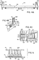
- the connector 90 generally comprises a housing 92 and electrical contacts 94.
- the housing 92 is made of dielectric material, such as molded polymer or plastic material.
- the housing 92 has an elongate center section 96 and two end sections 98.
- the center section 96 has a card edge receiving slot 100 and contact channels 102.
- the end sections 98 are basically mirror images of each other and each includes a raised post section 104.
- Each post section 104 has a tapered base 106, an end portion 108 extending up from the tapered base 106, and two opposing side guides 110 also extending up from the tapered base 106.
- the end portion 108 and side guides 110 all extend up from the tapered base 106 in general cantilever fashion.
- the interior sides of the side guides 110 have interference stabilizer projections 112.
- Area 114 between the two side guides 110 is adapted to receive a portion of a daughter printed circuit board therein.
- the projections 112 are adapted to make an interference gripping with a daughter board inserted into area 114.
- the end sections 98 are thus able to function as guides for allowing proper insertion of the daughter board into the card edge receiving slot 100. Because the depth of the slot 100 is so small, the end sections 98 also function as stabilizers for the daughter board on the housing.
- the interference between the projections 112 and the daughter board functions to frictionally retain the daughter board to the connector 90.
- the contacts 94 are made of electrically conductive material and are mounted to the housing 92 in the contact channels 102.
- the contacts 94 have tail ends 116 that extend out of the bottom of the housing 92.
- the tail ends 116 function as through-hole solder tails.
- the rest of the contacts are located in the housing with contact areas 118 extending into the card edge receiving slot 100.
- the widest portion of the contact 94 is located at its top 120 where it is bent.
- the width of each contact 94 progressively decreases on both sides of the contact away from the top bend 120. This shape is provided for uniform stress distribution on the contact. However, any suitable contacts could be provided.
- a plurality of the connectors 90 are shown connected to a first mother board 14 and sandwiched under a second mother board 16. As seen, the connectors 90 are compactly connected next to each other; side-by-side. The gap 122 between exterior sides of the connectors 90 may even be zero. However, because of the unique shapes of the post sections 104 relatively wide open areas 124 are formed between the post sections 104 of adjacent connectors 90 at end sections 98. These relatively wide open areas 124 allow air to circulate. Thus, daughter boards mounted in the connectors 90 can have better cooling air flow in the otherwise confined and congested area between the two boards 14, 16. The shape of the post sections 104 not only function as guides, stabilizers and retainers for the daughter boards, but they also allow good cooling air flow to the daughter boards mounted to the series of connectors.
- FIG. 6 a perspective view of an end of an alternate embodiment of the present invention is shown.
- the connector 130 is shown with a partial view of a daughter board 19 connected thereto.
- the connector 130 is similar to the connector shown in Figs. 4A-4C, but with several differences.
- the tail ends 132 of the contacts 134 are surface mount solder tails.
- the end section 138 of the housing 140 has a raised post section 139 (shown partially cut-away).
- the end section 138 also has a receiving area 141 for operably mounting an ejector 142.
- the receiving area 141 is generally established by two side sections 144, 145, a bottom rail 146 between the two side sections 144, 145, and two retaining projections 148, 149 extending from the two side sections 144, 145 towards each other at the top of the receiving area 141.
- the raised post section 139 is substantially similar to the raised post sections 104 of the embodiment shown in Figs. 4A-4C. However, the end portion 143 of the raised post section 139 stops below cantilevered extension 164.
- the ejector 142 generally comprises an ejector foot 150, a finger contact section 152, and a mounting section 154.
- the foot 150 includes a top surface 156 that the bottom surface of the daughter board 19 rests against.
- the mounting section 154 has a bottom pivot surface 158, two top side ledges 160, 161, and a stop 162 at a front end of each of the side ledges 160, 161.
- the finger contact section 152 has a cantilevered extension 164.
- the ejector 142 is snap-lock mounted into the receiving area 141 with bottom pivot surface 158 resting on the bottom rail 146.
- the two top side ledges 160, 161 are located under the projections 148, 149. In this fashion, the mounting section 154 is retained between the projections 148, 149 and the bottom rail 146.
- the ejector 142 can pivot at the mounting section 154 relative to the housing 140 in order to move the ejector foot 150.
- the stops 162 (only one of which is shown) limit the pivotal movement of the ejector when they come into contact with the fronts of the projections 148, 149.
- the cantilevered extension 164 is adapted to project into notch 166 in the daughter board 19.
- the ejector 142 is made of a suitable resilient deflectable material, such as a plastic or polymer material.
- the extension 164 is suitably shaped and has a suitable distance above the bottom of the card receiving slot 168 such that, when the card 19 is inserted in the slot 168 and the ejector is closed, the extension 164 projects into the notch 166 and is deflected slightly upward by the card 19 at the notch.
- the extension 164 is thus adapted to bias the card 19 downward against the bottom of the slot 168. In this fashion, the card 19 is prevented from moving in the slot 168. This prevents fretting corrosion from occurring between contacts on the card 19 and contacts of the connector 130 in the slot 168.
- the connector can be used with or without the ejectors 142. In this fashion, the assembler of an electronic device can configure the connector to suit the needs of the electronic device. This can obviously reduce the cost of the electronic device.
- FIG. 7A there is shown an elevational end view of an alternate embodiment of the present invention with a DIMM (Dual In-Line Memory Module) 174 connected to it.
- the connector 170 has end sections 172 with raised post sections 178 substantially similar to the end sections 98 of the embodiment shown in Figs. 4A-4C and 5.
- the connector 170 is an angled connector, similar to the connectors shown in Fig. 1, with the raised post sections 178 angled relative to the bottom surface 180 of the housing but without ejectors.
- a plurality of connectors 170 are shown connected to a first board 14 under a second board 16.
- the shape of the end sections 172 provide a greater air flow path by providing relatively open areas 176 between the connectors 170, but still allows the distance between the two boards 14, 16 to be very small. The distance or pitch between the connectors 170 is also kept small.
Landscapes
- Coupling Device And Connection With Printed Circuit (AREA)
- Details Of Connecting Devices For Male And Female Coupling (AREA)
Applications Claiming Priority (2)
| Application Number | Priority Date | Filing Date | Title |
|---|---|---|---|
| US260881 | 1994-06-16 | ||
| US08/260,881 US5511985A (en) | 1994-06-16 | 1994-06-16 | Angled card edge connector |
Publications (3)
| Publication Number | Publication Date |
|---|---|
| EP0688067A2 true EP0688067A2 (de) | 1995-12-20 |
| EP0688067A3 EP0688067A3 (de) | 1996-06-19 |
| EP0688067B1 EP0688067B1 (de) | 2000-04-05 |
Family
ID=22991038
Family Applications (1)
| Application Number | Title | Priority Date | Filing Date |
|---|---|---|---|
| EP95109385A Expired - Lifetime EP0688067B1 (de) | 1994-06-16 | 1995-06-16 | Winkelverbinder für Leiterplatten |
Country Status (4)
| Country | Link |
|---|---|
| US (1) | US5511985A (de) |
| EP (1) | EP0688067B1 (de) |
| JP (1) | JPH088004A (de) |
| DE (1) | DE69516042T2 (de) |
Cited By (6)
| Publication number | Priority date | Publication date | Assignee | Title |
|---|---|---|---|---|
| EP0871257A3 (de) * | 1997-04-11 | 1999-08-25 | Berg Electronics Manufacturing B.V. | Elektrischer Steckverbinder |
| US8029300B2 (en) | 2009-10-02 | 2011-10-04 | Research In Motion Limited | Connector and system for connectors |
| EP2309413B1 (de) * | 2009-10-02 | 2012-08-08 | Research In Motion Limited | Winkelsteckverbinder und System für Mobilanordnung |
| EP2635100A1 (de) * | 2012-02-29 | 2013-09-04 | Fifthplay NV | Montagesystem für elektronische Module |
| WO2016095635A1 (zh) * | 2014-12-17 | 2016-06-23 | 奥托立夫开发公司 | 汽车安全系统电控单元 |
| CN107799935A (zh) * | 2016-09-06 | 2018-03-13 | 富士康(昆山)电脑接插件有限公司 | 卡缘连接器及其组合 |
Families Citing this family (43)
| Publication number | Priority date | Publication date | Assignee | Title |
|---|---|---|---|---|
| US5672069A (en) * | 1995-11-13 | 1997-09-30 | Hon Hai Precision Ind. Co., Ltd. | Connector with ejector |
| US5730611A (en) * | 1996-07-01 | 1998-03-24 | Hon Hai Precision Ind. Co., Ltd. | Card edge connector with protective hidden locking lug of ejector |
| JPH10112360A (ja) * | 1996-10-08 | 1998-04-28 | Hirose Electric Co Ltd | 電気コネクタ |
| SG71046A1 (en) | 1996-10-10 | 2000-03-21 | Connector Systems Tech Nv | High density connector and method of manufacture |
| US6004142A (en) * | 1997-03-04 | 1999-12-21 | Micron Technology, Inc. | Interposer converter to allow single-sided contact to circuit modules |
| US6710614B1 (en) * | 1997-03-04 | 2004-03-23 | Micron Technology, Inc. | Methods for using an interposer/converter to allow single-sided contact to circuit modules |
| JPH10302863A (ja) * | 1997-04-25 | 1998-11-13 | Molex Inc | 基板取付型電気コネクタ |
| JP2002500810A (ja) * | 1997-05-27 | 2002-01-08 | ザ ウィタカー コーポレーション | カードエッジコネクタ及びコンタクト |
| US5961346A (en) * | 1997-07-30 | 1999-10-05 | Hon Hai Precision Inc. Co., Ltd. | Boardlock for use with slanted card edge connector |
| US5964606A (en) * | 1997-07-30 | 1999-10-12 | Hon Hai Precision Ind. Co., Ltd. | Structure of slanted DIMM connector for dense arrangement |
| US6012952A (en) * | 1997-08-13 | 2000-01-11 | Hon Hai Precision Ind. Co., Ltd. | Slanted connector |
| US6132228A (en) * | 1998-05-26 | 2000-10-17 | Molex Incorporated | Lever for card edge connector |
| JP2000215952A (ja) * | 1999-01-25 | 2000-08-04 | Yamaichi Electronics Co Ltd | カ―ドコネクタの実装構造 |
| TW431670U (en) * | 1999-05-06 | 2001-04-21 | Hon Hai Prec Ind Co Ltd | Electric connector |
| US6420514B1 (en) | 2000-07-12 | 2002-07-16 | Vision - Ease Lens, Inc. | Transparent polysulfone articles with reduced spurious coloration |
| JP4527310B2 (ja) * | 2000-12-08 | 2010-08-18 | タイコエレクトロニクスジャパン合同会社 | カードエッジコネクタ |
| AU2003230919B2 (en) * | 2002-04-15 | 2009-04-09 | Solvay Advanced Polymers, Llc | Polysulfone compositions exhibiting very low color and high light transmittance properties and articles made therefrom |
| TW537537U (en) * | 2002-07-10 | 2003-06-11 | Hon Hai Prec Ind Co Ltd | Electrical connector |
| JP3884343B2 (ja) * | 2002-07-18 | 2007-02-21 | タイコエレクトロニクスアンプ株式会社 | カード用コネクタ組立体 |
| JP4622778B2 (ja) * | 2005-09-26 | 2011-02-02 | 株式会社デンソー | 車両用計器の配線基板構造 |
| CN2874841Y (zh) * | 2005-10-21 | 2007-02-28 | 富士康(昆山)电脑接插件有限公司 | 电连接器 |
| US7458821B2 (en) * | 2005-12-07 | 2008-12-02 | Intel Corporation | Electrical interface for memory connector |
| JP4711194B2 (ja) * | 2006-03-14 | 2011-06-29 | 日本電気株式会社 | 回路基板装置及びコネクタの挿抜方法 |
| TW200805805A (en) * | 2006-07-10 | 2008-01-16 | Fci Connectors Singapore Pte | Card edge connector and latch thereof |
| CN200959382Y (zh) * | 2006-09-05 | 2007-10-10 | 富士康(昆山)电脑接插件有限公司 | 卡缘连接器 |
| CN201041841Y (zh) * | 2007-03-09 | 2008-03-26 | 富士康(昆山)电脑接插件有限公司 | 卡缘连接器 |
| US20090007048A1 (en) * | 2007-04-11 | 2009-01-01 | Moises Cases | Design structure for a computer memory system with a shared memory module junction connector |
| US7500863B2 (en) * | 2007-06-19 | 2009-03-10 | Tyco Electronics Corporation | DIMM socket positive lock extractor |
| CN201112942Y (zh) * | 2007-10-12 | 2008-09-10 | 富士康(昆山)电脑接插件有限公司 | 电连接器 |
| US7993147B2 (en) * | 2009-02-16 | 2011-08-09 | Tyco Electronics Corporation | Card edge module connector assembly |
| JP5293416B2 (ja) * | 2009-06-02 | 2013-09-18 | 富士通株式会社 | 接触端子およびコネクタ |
| RU2544839C2 (ru) | 2010-05-28 | 2015-03-20 | Эппл Инк. | Соединитель с двойной ориентацией с внешними контактами |
| KR101735646B1 (ko) * | 2010-08-09 | 2017-05-25 | 삼성전자주식회사 | 영상처리보드 및 이를 갖춘 디스플레이장치 |
| US8425237B2 (en) * | 2010-09-11 | 2013-04-23 | International Business Machines Corporation | Socket having heat-dissipating vents |
| CN201927742U (zh) * | 2010-11-01 | 2011-08-10 | 富士康(昆山)电脑接插件有限公司 | 卡缘连接器 |
| CN202930658U (zh) * | 2011-08-12 | 2013-05-08 | Fci公司 | 电连接器和电连接器组件 |
| CN203166226U (zh) * | 2011-08-12 | 2013-08-28 | Fci公司 | 电缆连接器 |
| US8708745B2 (en) | 2011-11-07 | 2014-04-29 | Apple Inc. | Dual orientation electronic connector |
| US20140206209A1 (en) | 2013-01-24 | 2014-07-24 | Apple Inc. | Reversible usb connector |
| CN108574176B (zh) | 2017-03-07 | 2020-08-25 | 美国莫列斯有限公司 | 电连接器 |
| TWI600214B (zh) * | 2017-03-07 | 2017-09-21 | 莫仕有限公司 | 電連接器 |
| US10218097B2 (en) * | 2017-07-11 | 2019-02-26 | Te Connectivity Corporation | Card edge connector assembly |
| US12444869B2 (en) * | 2022-12-14 | 2025-10-14 | International Business Machines Corporation | Coplanar card-edge connector |
Citations (12)
| Publication number | Priority date | Publication date | Assignee | Title |
|---|---|---|---|---|
| US3767974A (en) | 1972-01-03 | 1973-10-23 | Cogar Corp | Insertion and extraction lever for printed circuit cards |
| US4070081A (en) | 1975-10-13 | 1978-01-24 | Yamaichi Electric Mfg., Co., Ltd. | Coupling mechanism for male and female connectors |
| US4241966A (en) | 1979-04-26 | 1980-12-30 | Thomas & Betts Corporation | Connector with ejector-retainer means |
| US4473263A (en) | 1981-01-21 | 1984-09-25 | Sunstein Drew E | Circuit board mounting device and associated components |
| US4579408A (en) | 1983-04-11 | 1986-04-01 | Oki Densen Kabushiki Kaisha | Electrical connector structure with release and locking mechanism |
| US4756694A (en) | 1986-12-19 | 1988-07-12 | Amp Incorporated | Dual row connector for low profile package |
| US4862400A (en) | 1987-05-28 | 1989-08-29 | CTXT Systems, Inc. | Microcomputer bus assembly |
| US4898540A (en) | 1987-12-28 | 1990-02-06 | Yamaichi Electric Mfg. Co., Ltd. | Connector for a printed circuit board |
| US4973255A (en) | 1989-09-11 | 1990-11-27 | Itt Corporation | Locking/ejecting mechanism for connector system |
| US4975073A (en) | 1989-02-13 | 1990-12-04 | Calmark Corporation | Insertion and extraction aid for printed circuit card |
| US5074800A (en) | 1989-12-04 | 1991-12-24 | Molex Incorporated | Locking type ejection lever for use in a card edge connector |
| US5167517A (en) | 1991-12-05 | 1992-12-01 | Long Frank T | Ejecting SIMM socket |
Family Cites Families (13)
| Publication number | Priority date | Publication date | Assignee | Title |
|---|---|---|---|---|
| US4178051A (en) * | 1978-06-21 | 1979-12-11 | Amp Incorporated | Latch/eject pin header |
| FR2469019A1 (fr) * | 1979-10-26 | 1981-05-08 | Socapex | Support pour carte enfichable a raccordement electrique et thermique |
| US4445740A (en) * | 1982-04-26 | 1984-05-01 | Rockwell International Corporation | Circuit board assembly |
| US5162002A (en) * | 1990-03-30 | 1992-11-10 | Molex Incorporated | Card edge connector assembly |
| US5100337A (en) * | 1991-01-22 | 1992-03-31 | Lee Chao Kuei L | Electrical connector for exerting multiple elastic forces |
| US5174780A (en) * | 1991-03-29 | 1992-12-29 | Yang Lee Su Lan | Slant socket for memory module |
| US5061201A (en) * | 1991-04-08 | 1991-10-29 | Kenny Tuan | Contact element of electrical connector having high clamping force |
| US5254017A (en) * | 1991-09-13 | 1993-10-19 | Robinson Nugent, Inc. | Terminal for low profile edge socket |
| US5259768A (en) * | 1992-03-24 | 1993-11-09 | Molex Incorporated | Impedance and inductance control in electrical connectors and including reduced crosstalk |
| JP2761489B2 (ja) * | 1992-04-06 | 1998-06-04 | モレックス インコーポレーテッド | 電気コネクタ |
| US5199907A (en) * | 1992-06-18 | 1993-04-06 | Amp Incorporated | Electrical connector having contacts with board retention feature |
| US5364282A (en) * | 1993-08-16 | 1994-11-15 | Robinson Nugent, Inc. | Electrical connector socket with daughtercard ejector |
| US5389000A (en) * | 1993-11-18 | 1995-02-14 | Molex Incorporated | Edge card connector with improved latch/eject mechanism |
-
1994
- 1994-06-16 US US08/260,881 patent/US5511985A/en not_active Expired - Fee Related
-
1995
- 1995-06-02 JP JP7137015A patent/JPH088004A/ja not_active Withdrawn
- 1995-06-16 EP EP95109385A patent/EP0688067B1/de not_active Expired - Lifetime
- 1995-06-16 DE DE69516042T patent/DE69516042T2/de not_active Expired - Fee Related
Patent Citations (12)
| Publication number | Priority date | Publication date | Assignee | Title |
|---|---|---|---|---|
| US3767974A (en) | 1972-01-03 | 1973-10-23 | Cogar Corp | Insertion and extraction lever for printed circuit cards |
| US4070081A (en) | 1975-10-13 | 1978-01-24 | Yamaichi Electric Mfg., Co., Ltd. | Coupling mechanism for male and female connectors |
| US4241966A (en) | 1979-04-26 | 1980-12-30 | Thomas & Betts Corporation | Connector with ejector-retainer means |
| US4473263A (en) | 1981-01-21 | 1984-09-25 | Sunstein Drew E | Circuit board mounting device and associated components |
| US4579408A (en) | 1983-04-11 | 1986-04-01 | Oki Densen Kabushiki Kaisha | Electrical connector structure with release and locking mechanism |
| US4756694A (en) | 1986-12-19 | 1988-07-12 | Amp Incorporated | Dual row connector for low profile package |
| US4862400A (en) | 1987-05-28 | 1989-08-29 | CTXT Systems, Inc. | Microcomputer bus assembly |
| US4898540A (en) | 1987-12-28 | 1990-02-06 | Yamaichi Electric Mfg. Co., Ltd. | Connector for a printed circuit board |
| US4975073A (en) | 1989-02-13 | 1990-12-04 | Calmark Corporation | Insertion and extraction aid for printed circuit card |
| US4973255A (en) | 1989-09-11 | 1990-11-27 | Itt Corporation | Locking/ejecting mechanism for connector system |
| US5074800A (en) | 1989-12-04 | 1991-12-24 | Molex Incorporated | Locking type ejection lever for use in a card edge connector |
| US5167517A (en) | 1991-12-05 | 1992-12-01 | Long Frank T | Ejecting SIMM socket |
Cited By (9)
| Publication number | Priority date | Publication date | Assignee | Title |
|---|---|---|---|---|
| EP0871257A3 (de) * | 1997-04-11 | 1999-08-25 | Berg Electronics Manufacturing B.V. | Elektrischer Steckverbinder |
| US6033253A (en) * | 1997-04-11 | 2000-03-07 | Berg Technology, Inc. | Electrical connector with guide and latch |
| US8029300B2 (en) | 2009-10-02 | 2011-10-04 | Research In Motion Limited | Connector and system for connectors |
| EP2309413B1 (de) * | 2009-10-02 | 2012-08-08 | Research In Motion Limited | Winkelsteckverbinder und System für Mobilanordnung |
| EP2635100A1 (de) * | 2012-02-29 | 2013-09-04 | Fifthplay NV | Montagesystem für elektronische Module |
| BE1020549A3 (nl) * | 2012-02-29 | 2013-12-03 | Fifthplay N V | Montagesysteem voor elektronische modules. |
| WO2016095635A1 (zh) * | 2014-12-17 | 2016-06-23 | 奥托立夫开发公司 | 汽车安全系统电控单元 |
| CN107799935A (zh) * | 2016-09-06 | 2018-03-13 | 富士康(昆山)电脑接插件有限公司 | 卡缘连接器及其组合 |
| CN107799935B (zh) * | 2016-09-06 | 2019-08-30 | 富士康(昆山)电脑接插件有限公司 | 卡缘连接器及其组合 |
Also Published As
| Publication number | Publication date |
|---|---|
| EP0688067B1 (de) | 2000-04-05 |
| US5511985A (en) | 1996-04-30 |
| EP0688067A3 (de) | 1996-06-19 |
| DE69516042T2 (de) | 2000-08-03 |
| JPH088004A (ja) | 1996-01-12 |
| DE69516042D1 (de) | 2000-05-11 |
Similar Documents
| Publication | Publication Date | Title |
|---|---|---|
| US5511985A (en) | Angled card edge connector | |
| US7794259B2 (en) | Electrical connector assembly for miniaturization | |
| EP0526861B1 (de) | Randverbinder für Leiterkarten | |
| US7491089B2 (en) | Connector guide member | |
| US5162002A (en) | Card edge connector assembly | |
| US5389000A (en) | Edge card connector with improved latch/eject mechanism | |
| US8435052B2 (en) | Connector with a housing pivotally supporting floating terminals | |
| EP0251508A1 (de) | Null-Einschubskraft-Schaltkartensteckverbinder | |
| US4973270A (en) | Circuit panel socket with cloverleaf contact | |
| US7402080B2 (en) | Electrical connector for reliably mounted on a printed circuit board | |
| US7427208B2 (en) | Electrical connector | |
| US6183273B1 (en) | Stacked electrical card connector assembly | |
| US7182618B1 (en) | PC board assembly | |
| US5514002A (en) | Electrical connector assembly and contacts therein | |
| US5259795A (en) | Edge connector for a printed circuit board or the like | |
| US20090111296A1 (en) | Latching device used for locking two daughter printed circuit boards in connector set | |
| US6293805B1 (en) | Board to board connector | |
| US5076804A (en) | Electrical connector assembly for mounting on a printed circuit board | |
| US5154627A (en) | Electrical connector insertably fixed with simplified metal latches | |
| US20070123087A1 (en) | Electrical connector | |
| US5509826A (en) | Very low profile card edge connector | |
| US6116917A (en) | Connector with floating spacer | |
| EP0529345B1 (de) | Leiterplatten-Randverbinder | |
| US6431898B1 (en) | Card connector | |
| EP0400378B1 (de) | Leiterplattensockel mit Kleeblattkontakt |
Legal Events
| Date | Code | Title | Description |
|---|---|---|---|
| PUAI | Public reference made under article 153(3) epc to a published international application that has entered the european phase |
Free format text: ORIGINAL CODE: 0009012 |
|
| AK | Designated contracting states |
Kind code of ref document: A2 Designated state(s): BE DE FR |
|
| PUAL | Search report despatched |
Free format text: ORIGINAL CODE: 0009013 |
|
| AK | Designated contracting states |
Kind code of ref document: A3 Designated state(s): BE CH DE DK ES FR GB IT LI NL SE |
|
| 17P | Request for examination filed |
Effective date: 19961209 |
|
| 17Q | First examination report despatched |
Effective date: 19980306 |
|
| GRAG | Despatch of communication of intention to grant |
Free format text: ORIGINAL CODE: EPIDOS AGRA |
|
| GRAG | Despatch of communication of intention to grant |
Free format text: ORIGINAL CODE: EPIDOS AGRA |
|
| GRAH | Despatch of communication of intention to grant a patent |
Free format text: ORIGINAL CODE: EPIDOS IGRA |
|
| GRAH | Despatch of communication of intention to grant a patent |
Free format text: ORIGINAL CODE: EPIDOS IGRA |
|
| RBV | Designated contracting states (corrected) |
Designated state(s): BE DE FR |
|
| GRAA | (expected) grant |
Free format text: ORIGINAL CODE: 0009210 |
|
| AK | Designated contracting states |
Kind code of ref document: B1 Designated state(s): BE DE FR |
|
| RIC1 | Information provided on ipc code assigned before grant |
Free format text: 7H 01R 12/18 A |
|
| REF | Corresponds to: |
Ref document number: 69516042 Country of ref document: DE Date of ref document: 20000511 |
|
| ET | Fr: translation filed | ||
| PLBE | No opposition filed within time limit |
Free format text: ORIGINAL CODE: 0009261 |
|
| STAA | Information on the status of an ep patent application or granted ep patent |
Free format text: STATUS: NO OPPOSITION FILED WITHIN TIME LIMIT |
|
| 26N | No opposition filed | ||
| PGFP | Annual fee paid to national office [announced via postgrant information from national office to epo] |
Ref country code: BE Payment date: 20010620 Year of fee payment: 7 |
|
| PGFP | Annual fee paid to national office [announced via postgrant information from national office to epo] |
Ref country code: FR Payment date: 20010627 Year of fee payment: 7 |
|
| PGFP | Annual fee paid to national office [announced via postgrant information from national office to epo] |
Ref country code: DE Payment date: 20010830 Year of fee payment: 7 |
|
| PG25 | Lapsed in a contracting state [announced via postgrant information from national office to epo] |
Ref country code: BE Free format text: LAPSE BECAUSE OF NON-PAYMENT OF DUE FEES Effective date: 20020630 |
|
| BERE | Be: lapsed |
Owner name: *FRAMATOME CONNECTORS INTERNATIONAL Effective date: 20020630 |
|
| PG25 | Lapsed in a contracting state [announced via postgrant information from national office to epo] |
Ref country code: DE Free format text: LAPSE BECAUSE OF NON-PAYMENT OF DUE FEES Effective date: 20030101 |
|
| PG25 | Lapsed in a contracting state [announced via postgrant information from national office to epo] |
Ref country code: FR Free format text: LAPSE BECAUSE OF NON-PAYMENT OF DUE FEES Effective date: 20030228 |
|
| REG | Reference to a national code |
Ref country code: FR Ref legal event code: ST |