EP0688068B1 - Connecteur électrique pour montage sur une plaquette à circuits imprimés - Google Patents
Connecteur électrique pour montage sur une plaquette à circuits imprimés Download PDFInfo
- Publication number
- EP0688068B1 EP0688068B1 EP95113733A EP95113733A EP0688068B1 EP 0688068 B1 EP0688068 B1 EP 0688068B1 EP 95113733 A EP95113733 A EP 95113733A EP 95113733 A EP95113733 A EP 95113733A EP 0688068 B1 EP0688068 B1 EP 0688068B1
- Authority
- EP
- European Patent Office
- Prior art keywords
- terminating
- sections
- face
- contacts
- housing
- Prior art date
- Legal status (The legal status is an assumption and is not a legal conclusion. Google has not performed a legal analysis and makes no representation as to the accuracy of the status listed.)
- Expired - Lifetime
Links
- 230000013011 mating Effects 0.000 claims description 14
- 238000005452 bending Methods 0.000 claims description 9
- 238000003780 insertion Methods 0.000 description 5
- 230000037431 insertion Effects 0.000 description 5
- 238000005476 soldering Methods 0.000 description 4
- 230000001934 delay Effects 0.000 description 2
- 230000000007 visual effect Effects 0.000 description 2
- 238000003491 array Methods 0.000 description 1
- 238000010276 construction Methods 0.000 description 1
- 239000003989 dielectric material Substances 0.000 description 1
- 230000000694 effects Effects 0.000 description 1
- 238000007689 inspection Methods 0.000 description 1
- 230000002452 interceptive effect Effects 0.000 description 1
- 239000004065 semiconductor Substances 0.000 description 1
Images



Classifications
-
- H—ELECTRICITY
- H01—ELECTRIC ELEMENTS
- H01R—ELECTRICALLY-CONDUCTIVE CONNECTIONS; STRUCTURAL ASSOCIATIONS OF A PLURALITY OF MUTUALLY-INSULATED ELECTRICAL CONNECTING ELEMENTS; COUPLING DEVICES; CURRENT COLLECTORS
- H01R12/00—Structural associations of a plurality of mutually-insulated electrical connecting elements, specially adapted for printed circuits, e.g. printed circuit boards [PCB], flat or ribbon cables, or like generally planar structures, e.g. terminal strips, terminal blocks; Coupling devices specially adapted for printed circuits, flat or ribbon cables, or like generally planar structures; Terminals specially adapted for contact with, or insertion into, printed circuits, flat or ribbon cables, or like generally planar structures
- H01R12/70—Coupling devices
- H01R12/71—Coupling devices for rigid printing circuits or like structures
- H01R12/712—Coupling devices for rigid printing circuits or like structures co-operating with the surface of the printed circuit or with a coupling device exclusively provided on the surface of the printed circuit
- H01R12/716—Coupling device provided on the PCB
-
- H—ELECTRICITY
- H01—ELECTRIC ELEMENTS
- H01R—ELECTRICALLY-CONDUCTIVE CONNECTIONS; STRUCTURAL ASSOCIATIONS OF A PLURALITY OF MUTUALLY-INSULATED ELECTRICAL CONNECTING ELEMENTS; COUPLING DEVICES; CURRENT COLLECTORS
- H01R12/00—Structural associations of a plurality of mutually-insulated electrical connecting elements, specially adapted for printed circuits, e.g. printed circuit boards [PCB], flat or ribbon cables, or like generally planar structures, e.g. terminal strips, terminal blocks; Coupling devices specially adapted for printed circuits, flat or ribbon cables, or like generally planar structures; Terminals specially adapted for contact with, or insertion into, printed circuits, flat or ribbon cables, or like generally planar structures
- H01R12/70—Coupling devices
- H01R12/71—Coupling devices for rigid printing circuits or like structures
- H01R12/72—Coupling devices for rigid printing circuits or like structures coupling with the edge of the rigid printed circuits or like structures
- H01R12/722—Coupling devices for rigid printing circuits or like structures coupling with the edge of the rigid printed circuits or like structures coupling devices mounted on the edge of the printed circuits
- H01R12/724—Coupling devices for rigid printing circuits or like structures coupling with the edge of the rigid printed circuits or like structures coupling devices mounted on the edge of the printed circuits containing contact members forming a right angle
Definitions
- This invention generally relates to the art of electrical connectors and, particularly, to a right angle header connector according to the preamble of claim 1.
- Header connectors are used with IC packs or memory cards for interconnecting the semi-conductor circuit of the IC pack to an external circuit such as a main electronic unit.
- the IC pack is inserted into the header connector and is extracted therefrom as needed.
- header connectors are configured for mounting on a surface of a printed circuit board.
- the connector includes a dielectric housing having a forward mating face from which contact sections of a plurality of contacts project for interconnection with the contacts of the IC pack.
- the housing has a bottom mounting face for mounting the connector on the printed circuit board and a rearward terminating face from which terminating sections of the contacts project for connection to corresponding circuit traces on the printed circuit board.
- the terminating sections may have contact pads for soldering to the circuit traces.
- the terminating sections of the contacts project from the rearward terminating face of the dielectric housing at equal angles and different distances from the housing for soldering to the circuit traces on the printed circuit board which are in different arrays on the surface of the board.
- the different overall lengths result in that the point of deflection of the terminating sections of the lower rows space closer to the rearward side of housing than the upper rows. This contemplates problems in providing sufficient flexibility for all of the terminating sections regardless of which row the respective contacts are located.
- lead coplanarity of surface mounted connectors may be optimized.
- Other problems involve providing surfaces on the terminating sections, outside the dielectric housing, without interfering with the rearward terminating face of the housing during terminal insertion.
- problems are encountered in header connectors of the character described in affording visual observation of the condition of the printed circuit board termiantions.
- This invention is directed to solving the above problems in a header connector apparatus of the character described and to provide a new and improved electrical connector for mounting on a surface of a printed circuit board, such as the header connector for interconnection with IC packs or memory cards.
- An object, therefore, of the invention is to provide a new and improved electrical connector for mounting on a surface of a printed circuit board, such as a header connector for interconnection with IC packs or memory cards.
- an electrical connector which includes a dielectric housing having a bottom surface for mounting on a surface of a printed circuit board.
- the housing includes a forward mating face and a rearward terminating face.
- a plurality of contact passages are provided in the housing extending between the forward mating face and the rearward terminating face and defining top and bottom rows and vertical columns of passages, with at least a pair of passages in each column.
- a plurality of contacts are secured in the passages and have contact sections projecting from the forward mating face for interconnection with mating contacts of an appropriate IC pack or memory card.
- the contacts have terminating sections projecting from the rearward terminating face of the housing for connection to corresponding circuit traces on the printed circuit board, as by soldering.
- the terminating sections of the contacts in the bottom row thereof are formed toward the printed circuit board at a first angle for connection to corresponding circuit traces spaced a given distance from the rearward terminating face.
- the terminating sections of the contacts in the top row thereof are formed toward the printed circuit board at an angle smaller than the first angle for connection to corresponding circuit traces which are spaced closer to the rearward terminating face than the bottom row contacts.
- the terminating sections of each terminal must project from the rearward terminating face at separate vertical planes. Therefore, in an embodiment of the invention, the terminating sections of the top and bottom rows are offset from one another.
- the terminating sections of the contacts in the bottom rows thereof project from the rearward terminating face of the housing generally in the planes of the respective columns of contacts.
- the terminating sections of the contacts in the top and bottom row in the same vertical plane project from the rearward terminating face offset from the plane opposite from one another.
- the relative angles and positions of the terminating sections of the top and bottom rows of the terminals allows all terminals to have the same overall length. This is important where the switching speed of the electrical signal in the system is increased. If the electrical pathlengths of the terminals varies, propagation of the signal is not uniform and signal delays may result between adjacent terminals.
- the constant overall length in applicants' invention assures equal pathlength of high speed electrical signals and therefore minimizes signal delay.
- the relative bending moment of the terminating sections in the top row of terminals is less than that of the terminating sections in the bottom row.
- the housing has a stepped configuration in the rearward terminating face thereof from which the terminating sections of the top row of contacts project. This effects an increase in the vertical flexibility of the top row leads and substantially equalizes the bending moments of the two rows of terminals, thus improving the coplanarity of the leads.
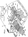
- a header connector apparatus generally designated 10 which includes a dielectric housing, generally designated 12, integrally molded of dielectric material such a plastic or the like.
- the housing mounts a plurality of high density contacts, generally designated 14, which include contact sections 16 and terminating sections 18.
- Contact sections 16 are provided for insertion into contact sockets of an IC pack or memory card (not shown) as is known in the art.
- Terminating sections 18 are adapted for connecting to corresponding circuit traces on a printed circuit board, as by soldering and as will be described hereinafter.
- Housing 12 has a pair of arms 20 defining tracks 22 for guiding a memory card into mating condition with an edge of the card inserted into a transverse receptacle 25 (Fig. 1) for mating of the contact sockets of the card with contact sections 16 of contacts 14 inserted into the contact sockets of the card.
- housing 12 has a forward mating face 24 (Fig. 1), a rearward terminating face 26 (Fig. 2) and a bottom mounting face 28.
- the bottom face is to be positioned on a surface of a printed circuit board, and means are provided for mounting the housing to the board.
- the housing includes a plurality of integral mounting pegs 30 projecting from bottom face 28 for insertion into appropriate mounting holes in the printed circuit board.
- arms 20 of the housing have vertical through slots 32 into which locking clips are inserted to lock the housing to the board.
- bifurcated locking legs 34 of the locking clips are visible projecting from bottom face 28 in line with slots 32.
- housing 12 has a plurality of contact passages 36 and 38 extending between forward mating face 24 and rearward terminating face 26.
- the contact passages define a top row (passages 36) and a bottom row (passages 38), with a pair of passages, one from each row, in a plurality of transverse columns.
- one passage 36 from the top row and a subjacent passage 38 from the bottom row are in a common vertical plane. Consequently, vertical pairs of contact sections 16 of terminals 14 are arranged in vertical pairs transversely of the housing and receptacle 25 therein.
- each top contact 14a has a terminating section 18a and each bottom contact 14b has a terminating section 18b.
- Each terminating section 18a and 18b has a distal end 40 which defines a contact area for engaging contact pads 42a and 42b on a printed circuit board 44 (Fig. 3).
- each contact 14a and 14b has a barbed section 46 which securely seats the contacts within passages 36 and 38. This is seen by the two pairs of contacts 14a and 14b shown in the cut away portion on the right side of Figure 3.
- each vertical pair of passages 36 and 38 and each corresponding vertical pair of contact sections 18 of a vertical pair of contacts 14a and 14b are arranged in a vertical plane.
- terminating sections 18a of contacts 14a and terminating sections 18b of contacts 14b are disposed on respective opposite sides of the respective plane.
- top contact 14a has a terminating section 18a to the right of the plane
- bottom contact 14b has a terminating section 18a to the left of the respective plane.
- each contact has a transverse shoulder or surface 48a for contacts 14a and 48b for contacts 14b. These shoulders or surfaces provide means for appropriate tooling to abut and drive or insert the contacts into their respective passages.
- terminating sections 18b of bottom contacts 14b are formed toward the printed circuit board 44 at a relatively large first angle for connection to corresponding circuit traces 42b spaced a given distance from rearward terminating face 26 of housing 12.
- Terminating sections 18a of top contacts 14a are formed toward the printed circuit board 44 at a relatively smaller angle than terminating sections 18b for connection to circuit traces 42a spaced closer to terminating face 26 than terminating sections 18b of contacts 14b.
- the relative angles and positions of the terminating sections of the top and bottom rows of the terminals allows all terminals 14 to have the same overall length. This is important where the switching speed of the electrical signal in the system is increased. If the electrical pathlengths of the terminals varies, propagation of the signal is not uniform and signal delays may result.
- the constant overall length in applicants' invention assures equal pathlength of high speed electrical signals and therefore minimizes signal delay.
- the relative bending moment of the terminating sections in the top row of terminals is less than that of the terminating sections in the bottom row.
- the terminating sections of those contacts had relatively smaller bending moments than those engaging circuit traces further from the housing.
- the flexibility of the leads and therefore the bending moments of the top row of terminals should be substantially equal to those of the bottom row in order to optimize the coplanarity of the leads.
- the invention contemplates means for solving this problem by providing a stepped configuration in the rearward terminating face of the housing which affords increased vertical flexibility for the smaller angled contacts.
- an area 50 of rearward terminating face 26 of housing 12 is recessed, as defined by a step 52, so that the open ends of upper passages 36 are spaced inwardly from the open ends of bottom passages 38.
- the portions of top contacts 14a which project outwardly from housing 12 are made longer to provide greater vertical flexibility for terminating sections 18a of the top contacts effectively increasing the bending moment of the upper row of contacts.
- the stepped configuration of the housing provides additional spacing about shoulders 48a of top contacts 14a to accommodate the insertion tooling which is used to insert the contacts into the passages of the housing.
- an open area is provided along rearward terminating face 26 to afford greater visual observation of the interconnections between pads 40 of the terminating sections of the top contacts 14a with circuit traces 42a on the printed circuit board, thereby providing easier inspection of the interconnections.
- FIG 4 shows an alternate construction of the bottom contacts in relation to top contacts 14a.
- bottom contacts generally designated 56, in Figure 4 again include contact sections 16, contact pads 40 and terminating sections now designated 58, with the terminating sections being in the same plane as contact sections 16 of any given pair of top and bottom contacts.
- top contacts 14a have offset terminating sections as shown in the drawing. This arrangement can accommodate circuit traces 42c and 42d which, may be staggered, with only terminating section 18a offset relative to the vertical plane of the contact sections while terminating sections 58 remain in the plane.
Landscapes
- Coupling Device And Connection With Printed Circuit (AREA)
- Multi-Conductor Connections (AREA)
Claims (6)
- Connecteur électrique (10) à angle droit pour montage sur une surface d'une carte à circuit imprimé (44) dans lequel le connecteur comprend :caractérisé :un boítier diélectrique (12) comportant une face inférieure (28) de montage, une face avant (24) d'accouplement et une face arrière (26) de raccordement,plusieurs conduits (36, 38) de borne situés dans le boítier et s'étendant entre la face avant (24) d'accouplement et la face arrière (26) de raccordement et définissant des rangées supérieure et inférieure et des colonnes verticales de conduits, au moins deux conduits se trouvant dans chaque colonne, et une pluralité de bornes conductrices (14) fixées dans les conduits, chacune comportant une section (16) de contact en saillie de ladite face avant (24) d'accouplement et une section (18, 58) de raccordement en saillie de la face arrière (26) de raccordement comprenant une extrémité (40) de coopération de carte pouvant être connectée avec des rubans de circuit correspondants (42) situés sur la carte à circuit imprimé (26),chaque section (18) de raccordement définissant un bras de montage fléchissant autour d'un point, défini globalement entre la section (16) de contact et la section (18) de raccordement, en réponse à une force appliquée à l'extrémité de coopération de carte de la borne par la carte à circuit imprimé (44),en ce que l'angle des sections de raccordement de la rangée supérieure (18a) par rapport à la carte est plus grand que l'angle des sections de raccordement de la rangée inférieure (18b, 58) par rapport à la carte,en ce que les bornes conductrices desdites rangées supérieure et inférieure ont sensiblement la même longueur hors tout, ce par quoi un signal électrique passant par chacune desdites bornes se déplacera sur environ la même distance pendant la même durée, en éliminant ainsi un retard de signal.
- Connecteur électrique (10) à angle droit selon la revendication 1, dans lequel les points de fléchissement des bras de montage des sections de raccordement de la rangée supérieure (18a, 58) sont décalés des points de fléchissement des bras de montage des sections de raccordement de la rangée inférieure (18b) dans la direction de la face avant (24) d'accouplement du boítier (12),
ce par quoi les moments fléchissants des bras de montage de la rangée supérieure sont sensiblement égaux aux moments fléchissants des bras de montage de la rangée inférieure. - Connecteur électrique (10) selon la revendication 1 ou 2, dans lequel les points de fléchissement des bras de montage des sections de raccordement des rangées supérieure et inférieure sont définis par la partie de la face arrière de raccordement surjacente au conduit de borne respectif.
- Connecteur électrique selon la revendication 1, 2 ou 3, dans lequel une zone (50) de la face arrière (26) de raccordement est évidée de manière étagée (52), de façon que les extrémités ouvertes de conduits supérieurs (36) soient écartées vers l'intérieur des extrémités ouvertes de conduits inférieurs (38).
- Connecteur électrique (10) selon l'une quelconque des revendications 1 à 4, dans lequel les sections de raccordement des contacts de sa rangée inférieure (58) font saillie de la face arrière (26) de raccordement du boítier, globalement dans les plans des colonnes respectives des sections de contact, et dans lequel les sections de raccordement des contacts de ses rangées supérieures (18a) font saillie de la face arrière (28) de raccordement du boítier, décalées par rapport auxdits plans.
- Connecteur électrique (10) selon l'une quelconque des revendications 1 à 4, dans lequel les sections de raccordement des contacts de sa rangée inférieure (18b) font saillie de la face arrière (26) de raccordement du boítier, décalées vers un côté des plans des colonnes respectives des sections de contact, et dans lequel les sections de raccordement des contacts de sa rangée supérieure (18a) font saillie de la face arrière (26) de raccordement du boítier, décalées vers le côté opposé desdits plans.
Applications Claiming Priority (3)
| Application Number | Priority Date | Filing Date | Title |
|---|---|---|---|
| US07/749,250 US5201662A (en) | 1991-08-23 | 1991-08-23 | Electrical connector for mounting on a printed circuit board |
| US749250 | 1991-08-23 | ||
| EP92113208A EP0529350B1 (fr) | 1991-08-23 | 1992-08-03 | Connecteur électrique pour montage sur une plaquette à circuits imprimés |
Related Parent Applications (1)
| Application Number | Title | Priority Date | Filing Date |
|---|---|---|---|
| EP92113208.0 Division | 1992-08-03 |
Publications (3)
| Publication Number | Publication Date |
|---|---|
| EP0688068A2 EP0688068A2 (fr) | 1995-12-20 |
| EP0688068A3 EP0688068A3 (fr) | 1997-02-26 |
| EP0688068B1 true EP0688068B1 (fr) | 1999-05-12 |
Family
ID=25012940
Family Applications (2)
| Application Number | Title | Priority Date | Filing Date |
|---|---|---|---|
| EP95113733A Expired - Lifetime EP0688068B1 (fr) | 1991-08-23 | 1992-08-03 | Connecteur électrique pour montage sur une plaquette à circuits imprimés |
| EP92113208A Expired - Lifetime EP0529350B1 (fr) | 1991-08-23 | 1992-08-03 | Connecteur électrique pour montage sur une plaquette à circuits imprimés |
Family Applications After (1)
| Application Number | Title | Priority Date | Filing Date |
|---|---|---|---|
| EP92113208A Expired - Lifetime EP0529350B1 (fr) | 1991-08-23 | 1992-08-03 | Connecteur électrique pour montage sur une plaquette à circuits imprimés |
Country Status (4)
| Country | Link |
|---|---|
| US (1) | US5201662A (fr) |
| EP (2) | EP0688068B1 (fr) |
| JP (1) | JP2649759B2 (fr) |
| DE (2) | DE69214569T2 (fr) |
Families Citing this family (44)
| Publication number | Priority date | Publication date | Assignee | Title |
|---|---|---|---|---|
| US5342208A (en) * | 1992-02-19 | 1994-08-30 | Nec Corporation | Package connector apparatus |
| US5318452A (en) * | 1992-08-10 | 1994-06-07 | The Whitaker Corporation | Electrical connector |
| US5297966A (en) * | 1992-08-10 | 1994-03-29 | The Whitaker Corporation | Mounting bracket for an electrical connector |
| US5230638A (en) * | 1992-08-12 | 1993-07-27 | Molex Incorporated | Surface mounted electrical connector for printed circuit boards |
| US5269694A (en) * | 1992-10-23 | 1993-12-14 | Molex Incorporated | Surface mount electrical connector |
| JP2575617Y2 (ja) * | 1993-01-14 | 1998-07-02 | 矢崎総業株式会社 | 回路基板用コネクタ |
| JP2567629Y2 (ja) | 1993-03-23 | 1998-04-02 | バーグ・テクノロジー・インコーポレーテッド | コネクタ装置 |
| EP0674812A4 (fr) * | 1993-09-16 | 1998-01-07 | Codex Inc | Fond de panier avec bus de signaux. |
| US5516297A (en) * | 1993-09-28 | 1996-05-14 | Kel Corporation | Surface mount electrical devices |
| DE4408693C2 (de) * | 1994-03-15 | 1996-10-31 | Stocko Metallwarenfab Henkels | Kontaktierungsvorrichtung |
| US5490786A (en) * | 1994-03-25 | 1996-02-13 | Itt Corporation | Termination of contact tails to PC board |
| JP3174578B2 (ja) * | 1994-04-28 | 2001-06-11 | ザ ウィタカー コーポレーション | 表面実装型のコンタクトを有する電気コネクタ |
| EP0689162A3 (fr) * | 1994-06-23 | 1996-02-07 | Molex Inc | Moyens de verrouillage pour l'assemblage d'une carte à circuit intégré |
| US5713747A (en) | 1995-01-06 | 1998-02-03 | Berg Technology, Inc. | Memory card connector |
| DE69627818T2 (de) * | 1995-01-06 | 2004-04-08 | Fci | Abgeschirmter speicherkartensteckverbinder |
| US5584709A (en) * | 1995-01-30 | 1996-12-17 | Molex Incorporated | Printed circuit board mounted electrical connector |
| JPH09139264A (ja) * | 1995-11-13 | 1997-05-27 | Yazaki Corp | Pcb用多極コネクタ |
| US5725386A (en) * | 1996-05-24 | 1998-03-10 | The Whitaker Corporation | Board-mountable electrical connector |
| US6135781A (en) * | 1996-07-17 | 2000-10-24 | Minnesota Mining And Manufacturing Company | Electrical interconnection system and device |
| EP0845750A3 (fr) * | 1996-11-29 | 2000-11-29 | Tyco Electronics Logistics AG | Connecteur double pour deux cartes à puce |
| US5885090A (en) * | 1997-03-21 | 1999-03-23 | Molex Incorporated | Electrical connector with stabilized offset spring arm |
| JP3405201B2 (ja) | 1998-06-17 | 2003-05-12 | 住友電装株式会社 | 機器用コネクタの製造方法 |
| JP2000067961A (ja) * | 1998-08-13 | 2000-03-03 | Molex Inc | 電気コネクタ |
| US6059610A (en) * | 1999-02-22 | 2000-05-09 | Chu; Ho-Kang | Board-to-board connector having retention mechanism |
| JP3227138B2 (ja) * | 1999-03-01 | 2001-11-12 | 日本圧着端子製造株式会社 | 高電圧用コネクタ |
| TW427571U (en) * | 1999-04-06 | 2001-03-21 | Hon Hai Prec Ind Co Ltd | Electrical connector |
| DE60014385T2 (de) | 1999-07-16 | 2006-02-23 | Molex Inc., Lisle | Impedanz-abgestimmter verbinder |
| US6280209B1 (en) | 1999-07-16 | 2001-08-28 | Molex Incorporated | Connector with improved performance characteristics |
| US6729891B2 (en) * | 2002-06-06 | 2004-05-04 | International Business Machines Corporation | Right angle board-to-board connector with balanced impedance |
| US7039417B2 (en) | 2003-09-25 | 2006-05-02 | Lenovo Pte Ltd | Apparatus, system, and method for mitigating access point data rate degradation |
| WO2004001907A1 (fr) | 2002-06-21 | 2003-12-31 | Molex Incorporated | Connecteur a reglage d'impedance haute densite presentant une structure modulaire |
| US6863549B2 (en) | 2002-09-25 | 2005-03-08 | Molex Incorporated | Impedance-tuned terminal contact arrangement and connectors incorporating same |
| US6796847B2 (en) * | 2002-10-21 | 2004-09-28 | Hubbell Incorporated | Electrical connector for telecommunications applications |
| GB2395372B (en) * | 2002-11-13 | 2005-08-31 | Contour Electronics Ltd | Connector |
| US6692273B1 (en) * | 2002-12-31 | 2004-02-17 | Hon Hai Precision Ind. Co., Ltd. | Straddle mount connector |
| DE602005003527T2 (de) * | 2004-09-29 | 2008-10-23 | Sumitomo Wiring Systems, Ltd., Yokkaichi | Ein Verbinder und Steckkontakt |
| WO2009025868A1 (fr) | 2007-08-23 | 2009-02-26 | Molex Incorporated | Connecteur électrique monté sur carte |
| EP2290753B1 (fr) * | 2009-08-31 | 2012-12-05 | ERNI Electronics GmbH | Connecteur et platine multicouche |
| DE102011089020B4 (de) * | 2011-12-19 | 2023-11-16 | Zf Friedrichshafen Ag | Kontaktverbinder und Verfahren zur Herstellung eines Kontaktverbinders |
| CN103326140B (zh) * | 2012-03-21 | 2016-03-02 | 富士康(昆山)电脑接插件有限公司 | 线缆连接器组件 |
| CN103326141B (zh) * | 2012-03-21 | 2016-02-03 | 富士康(昆山)电脑接插件有限公司 | 线缆连接器组件 |
| JP5367122B2 (ja) * | 2012-05-10 | 2013-12-11 | 日本航空電子工業株式会社 | コネクタ |
| JP2017224472A (ja) * | 2016-06-15 | 2017-12-21 | 株式会社オートネットワーク技術研究所 | 基板用コネクタ |
| JP7386147B2 (ja) * | 2020-11-06 | 2023-11-24 | ヒロセ電機株式会社 | 平型導体用電気コネクタ |
Family Cites Families (9)
| Publication number | Priority date | Publication date | Assignee | Title |
|---|---|---|---|---|
| US3384864A (en) * | 1965-11-15 | 1968-05-21 | Sperry Rand Corp | Electrical connector assembly |
| US4505035A (en) * | 1983-04-11 | 1985-03-19 | At&T Technologies, Inc. | Methods of aligning and mounting a plurality of electrical leads to a plurality of terminals |
| EP0147039A3 (fr) | 1983-12-13 | 1985-08-07 | AMP INCORPORATED (a New Jersey corporation) | Connecteur monté sur une surface |
| DE3603250A1 (de) * | 1986-02-03 | 1987-08-06 | Allied Corp | Steckverbinder, isolierkoerper dafuer und verfahren zur befestigung des steckverbinders an einer leiterplatte |
| US4734042A (en) * | 1987-02-09 | 1988-03-29 | Augat Inc. | Multi row high density connector |
| JPH0630273B2 (ja) * | 1988-02-23 | 1994-04-20 | トーマス アンド ベツツ コーポレーシヨン | 表面実装コネクタ |
| JPH0511664Y2 (fr) * | 1989-07-19 | 1993-03-23 | ||
| DE4027509C2 (de) * | 1990-08-30 | 1996-12-19 | Molex Inc | Vielpoliger Steckverbinder mit abgewinkelten Anschlußbeinen |
| JP2842679B2 (ja) * | 1990-09-20 | 1999-01-06 | 富士通株式会社 | 片面実装型コネクタ及びそれを用いた2ピース型icメモリカード |
-
1991
- 1991-08-23 US US07/749,250 patent/US5201662A/en not_active Expired - Fee Related
-
1992
- 1992-08-03 EP EP95113733A patent/EP0688068B1/fr not_active Expired - Lifetime
- 1992-08-03 DE DE69214569T patent/DE69214569T2/de not_active Expired - Fee Related
- 1992-08-03 DE DE69229185T patent/DE69229185T2/de not_active Expired - Fee Related
- 1992-08-03 EP EP92113208A patent/EP0529350B1/fr not_active Expired - Lifetime
- 1992-08-20 JP JP4244312A patent/JP2649759B2/ja not_active Expired - Lifetime
Also Published As
| Publication number | Publication date |
|---|---|
| DE69214569D1 (de) | 1996-11-21 |
| DE69229185T2 (de) | 2000-02-24 |
| JPH06119946A (ja) | 1994-04-28 |
| DE69229185D1 (de) | 1999-06-17 |
| EP0529350B1 (fr) | 1996-10-16 |
| EP0688068A3 (fr) | 1997-02-26 |
| DE69214569T2 (de) | 1997-02-20 |
| US5201662A (en) | 1993-04-13 |
| EP0529350A3 (en) | 1993-06-30 |
| EP0688068A2 (fr) | 1995-12-20 |
| JP2649759B2 (ja) | 1997-09-03 |
| EP0529350A2 (fr) | 1993-03-03 |
Similar Documents
| Publication | Publication Date | Title |
|---|---|---|
| EP0688068B1 (fr) | Connecteur électrique pour montage sur une plaquette à circuits imprimés | |
| US5161987A (en) | Connector with one piece ground bus | |
| US4686607A (en) | Daughter board/backplane assembly | |
| US6572409B2 (en) | Connector having a ground member obliquely extending with respect to an arrangement direction of a number of contacts | |
| US4867690A (en) | Electrical connector system | |
| US6435913B1 (en) | Header connector having two shields therein | |
| US9413112B2 (en) | Electrical connector having contact modules | |
| US9923309B1 (en) | PCB connector footprint | |
| EP2209170B1 (fr) | Système connecteur orthogonal | |
| EP1105940B1 (fr) | Dispositif de connexion | |
| EP0337634B1 (fr) | Conducteur de référence pour améliorer l'intégrité des signaux dans des connecteurs électriques | |
| US8157573B2 (en) | Connector | |
| US6238245B1 (en) | High speed, high density electrical connector | |
| US5201661A (en) | Printed circuit board flat flexible cable connector | |
| US5085601A (en) | Reduced insertion force electrical connector | |
| US7431616B2 (en) | Orthogonal electrical connectors | |
| US6231355B1 (en) | Matched impedance connector having retention device on a grounding plane | |
| US5695354A (en) | Printed circuit board connector | |
| KR100304515B1 (ko) | 고속에지형커넥터 | |
| JPH04272676A (ja) | 電気コネクタ | |
| EP0554003A1 (fr) | Socle d'allonge pour lecture duale | |
| JP2005530324A (ja) | 結合コネクタに設けるためのコネクタ及びそのためのシールド | |
| US5445529A (en) | Connector apparatus | |
| US20210104831A1 (en) | High density electrical connector | |
| US5876221A (en) | Surface mount contact assembly for printed circuit board |
Legal Events
| Date | Code | Title | Description |
|---|---|---|---|
| PUAI | Public reference made under article 153(3) epc to a published international application that has entered the european phase |
Free format text: ORIGINAL CODE: 0009012 |
|
| 17P | Request for examination filed |
Effective date: 19950906 |
|
| AC | Divisional application: reference to earlier application |
Ref document number: 529350 Country of ref document: EP |
|
| AK | Designated contracting states |
Kind code of ref document: A2 Designated state(s): DE FR GB IT |
|
| PUAL | Search report despatched |
Free format text: ORIGINAL CODE: 0009013 |
|
| AK | Designated contracting states |
Kind code of ref document: A3 Designated state(s): DE FR GB IT |
|
| GRAG | Despatch of communication of intention to grant |
Free format text: ORIGINAL CODE: EPIDOS AGRA |
|
| 17Q | First examination report despatched |
Effective date: 19980814 |
|
| GRAG | Despatch of communication of intention to grant |
Free format text: ORIGINAL CODE: EPIDOS AGRA |
|
| GRAH | Despatch of communication of intention to grant a patent |
Free format text: ORIGINAL CODE: EPIDOS IGRA |
|
| GRAH | Despatch of communication of intention to grant a patent |
Free format text: ORIGINAL CODE: EPIDOS IGRA |
|
| GRAA | (expected) grant |
Free format text: ORIGINAL CODE: 0009210 |
|
| AC | Divisional application: reference to earlier application |
Ref document number: 529350 Country of ref document: EP |
|
| AK | Designated contracting states |
Kind code of ref document: B1 Designated state(s): DE FR GB IT |
|
| REF | Corresponds to: |
Ref document number: 69229185 Country of ref document: DE Date of ref document: 19990617 |
|
| ET | Fr: translation filed | ||
| PGFP | Annual fee paid to national office [announced via postgrant information from national office to epo] |
Ref country code: FR Payment date: 19990802 Year of fee payment: 9 |
|
| PGFP | Annual fee paid to national office [announced via postgrant information from national office to epo] |
Ref country code: GB Payment date: 19990806 Year of fee payment: 8 |
|
| PGFP | Annual fee paid to national office [announced via postgrant information from national office to epo] |
Ref country code: DE Payment date: 19990927 Year of fee payment: 8 |
|
| PLBE | No opposition filed within time limit |
Free format text: ORIGINAL CODE: 0009261 |
|
| STAA | Information on the status of an ep patent application or granted ep patent |
Free format text: STATUS: NO OPPOSITION FILED WITHIN TIME LIMIT |
|
| 26N | No opposition filed | ||
| PG25 | Lapsed in a contracting state [announced via postgrant information from national office to epo] |
Ref country code: GB Free format text: LAPSE BECAUSE OF NON-PAYMENT OF DUE FEES Effective date: 20000803 |
|
| GBPC | Gb: european patent ceased through non-payment of renewal fee |
Effective date: 20000803 |
|
| PG25 | Lapsed in a contracting state [announced via postgrant information from national office to epo] |
Ref country code: DE Free format text: LAPSE BECAUSE OF NON-PAYMENT OF DUE FEES Effective date: 20010501 |
|
| PG25 | Lapsed in a contracting state [announced via postgrant information from national office to epo] |
Ref country code: FR Free format text: LAPSE BECAUSE OF NON-PAYMENT OF DUE FEES Effective date: 20020430 |
|
| REG | Reference to a national code |
Ref country code: FR Ref legal event code: ST |
|
| PG25 | Lapsed in a contracting state [announced via postgrant information from national office to epo] |
Ref country code: IT Free format text: LAPSE BECAUSE OF NON-PAYMENT OF DUE FEES;WARNING: LAPSES OF ITALIAN PATENTS WITH EFFECTIVE DATE BEFORE 2007 MAY HAVE OCCURRED AT ANY TIME BEFORE 2007. THE CORRECT EFFECTIVE DATE MAY BE DIFFERENT FROM THE ONE RECORDED. Effective date: 20050803 |