EP0689181A1 - Speicherschaltungen für räumliche Lichtmodulatoren - Google Patents
Speicherschaltungen für räumliche Lichtmodulatoren Download PDFInfo
- Publication number
- EP0689181A1 EP0689181A1 EP95109828A EP95109828A EP0689181A1 EP 0689181 A1 EP0689181 A1 EP 0689181A1 EP 95109828 A EP95109828 A EP 95109828A EP 95109828 A EP95109828 A EP 95109828A EP 0689181 A1 EP0689181 A1 EP 0689181A1
- Authority
- EP
- European Patent Office
- Prior art keywords
- pixels
- data
- memory cell
- modulator
- memory
- Prior art date
- Legal status (The legal status is an assumption and is not a legal conclusion. Google has not performed a legal analysis and makes no representation as to the accuracy of the status listed.)
- Granted
Links
- 238000000034 method Methods 0.000 claims description 17
- 230000004913 activation Effects 0.000 claims description 11
- 238000003491 array Methods 0.000 claims description 6
- 239000004973 liquid crystal related substance Substances 0.000 claims description 3
- 239000003990 capacitor Substances 0.000 claims description 2
- 210000004027 cell Anatomy 0.000 claims 13
- 210000002858 crystal cell Anatomy 0.000 claims 1
- 238000010586 diagram Methods 0.000 description 6
- 239000003086 colorant Substances 0.000 description 4
- 230000008901 benefit Effects 0.000 description 3
- 238000004519 manufacturing process Methods 0.000 description 3
- 230000008569 process Effects 0.000 description 2
- 230000004044 response Effects 0.000 description 2
- 241000953555 Theama Species 0.000 description 1
- 239000013078 crystal Substances 0.000 description 1
- 230000006870 function Effects 0.000 description 1
- 238000005286 illumination Methods 0.000 description 1
- 230000003287 optical effect Effects 0.000 description 1
- 238000012163 sequencing technique Methods 0.000 description 1
Images

Classifications
-
- G—PHYSICS
- G09—EDUCATION; CRYPTOGRAPHY; DISPLAY; ADVERTISING; SEALS
- G09G—ARRANGEMENTS OR CIRCUITS FOR CONTROL OF INDICATING DEVICES USING STATIC MEANS TO PRESENT VARIABLE INFORMATION
- G09G3/00—Control arrangements or circuits, of interest only in connection with visual indicators other than cathode-ray tubes
- G09G3/20—Control arrangements or circuits, of interest only in connection with visual indicators other than cathode-ray tubes for presentation of an assembly of a number of characters, e.g. a page, by composing the assembly by combination of individual elements arranged in a matrix no fixed position being assigned to or needed to be assigned to the individual characters or partial characters
- G09G3/34—Control arrangements or circuits, of interest only in connection with visual indicators other than cathode-ray tubes for presentation of an assembly of a number of characters, e.g. a page, by composing the assembly by combination of individual elements arranged in a matrix no fixed position being assigned to or needed to be assigned to the individual characters or partial characters by control of light from an independent source
- G09G3/3433—Control arrangements or circuits, of interest only in connection with visual indicators other than cathode-ray tubes for presentation of an assembly of a number of characters, e.g. a page, by composing the assembly by combination of individual elements arranged in a matrix no fixed position being assigned to or needed to be assigned to the individual characters or partial characters by control of light from an independent source using light modulating elements actuated by an electric field and being other than liquid crystal devices and electrochromic devices
- G09G3/346—Control arrangements or circuits, of interest only in connection with visual indicators other than cathode-ray tubes for presentation of an assembly of a number of characters, e.g. a page, by composing the assembly by combination of individual elements arranged in a matrix no fixed position being assigned to or needed to be assigned to the individual characters or partial characters by control of light from an independent source using light modulating elements actuated by an electric field and being other than liquid crystal devices and electrochromic devices based on modulation of the reflection angle, e.g. micromirrors
-
- G—PHYSICS
- G09—EDUCATION; CRYPTOGRAPHY; DISPLAY; ADVERTISING; SEALS
- G09G—ARRANGEMENTS OR CIRCUITS FOR CONTROL OF INDICATING DEVICES USING STATIC MEANS TO PRESENT VARIABLE INFORMATION
- G09G2300/00—Aspects of the constitution of display devices
- G09G2300/08—Active matrix structure, i.e. with use of active elements, inclusive of non-linear two terminal elements, in the pixels together with light emitting or modulating elements
- G09G2300/0804—Sub-multiplexed active matrix panel, i.e. wherein one active driving circuit is used at pixel level for multiple image producing elements
-
- G—PHYSICS
- G09—EDUCATION; CRYPTOGRAPHY; DISPLAY; ADVERTISING; SEALS
- G09G—ARRANGEMENTS OR CIRCUITS FOR CONTROL OF INDICATING DEVICES USING STATIC MEANS TO PRESENT VARIABLE INFORMATION
- G09G2300/00—Aspects of the constitution of display devices
- G09G2300/08—Active matrix structure, i.e. with use of active elements, inclusive of non-linear two terminal elements, in the pixels together with light emitting or modulating elements
- G09G2300/0809—Several active elements per pixel in active matrix panels
- G09G2300/0842—Several active elements per pixel in active matrix panels forming a memory circuit, e.g. a dynamic memory with one capacitor
-
- G—PHYSICS
- G09—EDUCATION; CRYPTOGRAPHY; DISPLAY; ADVERTISING; SEALS
- G09G—ARRANGEMENTS OR CIRCUITS FOR CONTROL OF INDICATING DEVICES USING STATIC MEANS TO PRESENT VARIABLE INFORMATION
- G09G2300/00—Aspects of the constitution of display devices
- G09G2300/08—Active matrix structure, i.e. with use of active elements, inclusive of non-linear two terminal elements, in the pixels together with light emitting or modulating elements
- G09G2300/0809—Several active elements per pixel in active matrix panels
- G09G2300/0842—Several active elements per pixel in active matrix panels forming a memory circuit, e.g. a dynamic memory with one capacitor
- G09G2300/0857—Static memory circuit, e.g. flip-flop
-
- G—PHYSICS
- G09—EDUCATION; CRYPTOGRAPHY; DISPLAY; ADVERTISING; SEALS
- G09G—ARRANGEMENTS OR CIRCUITS FOR CONTROL OF INDICATING DEVICES USING STATIC MEANS TO PRESENT VARIABLE INFORMATION
- G09G2310/00—Command of the display device
- G09G2310/06—Details of flat display driving waveforms
- G09G2310/061—Details of flat display driving waveforms for resetting or blanking
-
- G—PHYSICS
- G09—EDUCATION; CRYPTOGRAPHY; DISPLAY; ADVERTISING; SEALS
- G09G—ARRANGEMENTS OR CIRCUITS FOR CONTROL OF INDICATING DEVICES USING STATIC MEANS TO PRESENT VARIABLE INFORMATION
- G09G3/00—Control arrangements or circuits, of interest only in connection with visual indicators other than cathode-ray tubes
- G09G3/20—Control arrangements or circuits, of interest only in connection with visual indicators other than cathode-ray tubes for presentation of an assembly of a number of characters, e.g. a page, by composing the assembly by combination of individual elements arranged in a matrix no fixed position being assigned to or needed to be assigned to the individual characters or partial characters
- G09G3/2007—Display of intermediate tones
- G09G3/2018—Display of intermediate tones by time modulation using two or more time intervals
Definitions
- This invention relates to spatial light modulators, more particularly to memory schemes supporting spatial light modulator arrays.
- spatial light modulators consists of an array of individually addressable elements, such as liquid crystal display panels or digital micromirror devices. These examples of modulator arrays have many uses, such as printers, displays, and optical processing. This discussion will focus on display systems.
- these arrays function in binary mode, where each individual element receives either an ON or an OFF signal.
- the elements, or pixels, of the array that receive the ON signal form the image the viewer receives, either directly, from a screen or through optics.
- each modulator array must have circuitry allowing signals to reach each pixel and activate it to respond in a certain way.
- One approach requires one memory cell per pixel, where the memory cell receives the information for the pixel's next state. This information results from the scheme used to produce the displayed images.
- pulse width modulation One technique for production of images, called pulse width modulation, has each pixel turn ON and OFF repeatedly within a video frame time. This method controls the intensity of a given pixel by how many times within the frame the pixel is ON, or transmitting light to the final image. Digitally, gray levels are achieved by using weighted bits of data.
- each pixel receives 4 bits of data over the time period of one frame.
- the frame time is divided into 15 slices, 1-15.
- the most significant bit (MSB) would then receive 8 of those time slices for it to display its data.
- the next most significant bit would receive 4, etc.
- the above technique requires memory for keeping the data to be displayed and sending it to the pixel at the appropriate time.
- One technique uses one memory cell per pixel. The cell receives the pixel's data, the pixel gets a control signal allowing it to react to the new data is latched into its new state. Meanwhile, the cell is receiving the data for the pixel's next state. When the pixel transfer signal occurs, the pixel reacts to its new data.
- This particular technique uses less than one memory cell per pixel, with the number of pixels per memory cell called "fanout.”
- This architecture will be referred to more accurately as a multiplexed memory architecture.
- the memory cell receives the data for a set of pixels, rather than just one.
- One problem with the above approach is that the number of levels of intensity is linked to the number of pixels per memory cell.
- the number of pixels per memory cell must be determined before the device is fabricated.
- Using a device with a set fanout for a different number of bits of intensity increases the data rate, which eliminates the main advantage of using multiplexed memory architecture.
- An aspect of the invention is a spatial light modulator with an array of individually addressable pixels. Each pixel may be set and reset in response to a signal delivered to the pixel.
- a pixel consists of an active area, whether reflective or transmissive, and activation circuitry.
- the signals are passed to the pixels via a memory cell, with more than one pixel receiving from any one memory cell.
- the number of pixels in connection with a memory cell is decided before device fabrication, depending upon the number of bits of intensity.
- One aspect of the invention allows a device fabricated with a set number of pixels per memory cell to be used for several applications while minimizing the increase in the peak data rate.
- the same device could be used for two systems where each system uses a different number of bits of intensity, regardless of the fixed fanout of the device.
- Binary spatial light modulators are modulators with arrays of individually addressable pixels which have either an ON or OFF state. Examples are liquid crystal displays (LCD), digital micromirror devices (DMD), and actuated mirror arrays (AMA).
- LCD liquid crystal displays
- DMD digital micromirror devices
- AMA actuated mirror arrays
- PWM pulse-width modulation
- An incoming video data stream is digitized if necessary, and then passed to some type of memory.
- the memory stores the data stream by video frames.
- a given pixel on the array has a data in that video frame set specifically for that pixel.
- the size of the data set depends on the number of bits of intensity the system uses. If the system used 8 bits of intensity, there would be 8 bits of data for each pixel.
- the frame time is divided into 255 time slices.
- the most significant bit (MSB) receives 128 of these time slices for its display time.
- Display time means the time that a pixel is reacting to a given bit of data while receiving illumination.
- the data for that bit of significance may have one pixel in the ON position and another in the OFF position.
- the pixels assume either the ON or OFF positions depending upon the data on their activation circuitry.
- the activation circuitry normally consists of at least one electrode.
- the activation circuitry typically consists of piezo-electric crystals. Additionally, capacitors that can be charged and discharged can be used.
- the next MSB would then receive 64 time slices, and so on until the least significant bit (LSB) receives one time slice.
- LSB least significant bit
- the load time must equal one time slice. Since the LSB receives only one time slice, it is more common to refer to these time slices as the LSB time. After the pixels receive their data, they are latched into position for the appropriate number of LSB times. This allows the next bit of data to be loaded into the memory cell attached to each pixel. If the PWM scheme was very simple, and each bit was loaded in sequence MSB to LSB for one frame, the MSB of the next frame must be loaded in the LSB display time for the previous frame. Therefore, the load time must equal the LSB time.
- Adjustments can be made to lower the data rate, such as using two column drivers for each column, cutting the data rate in half. If the device used has 128 input pins, the columns could be grouped together to use a shift register that would allow the data rate to again be cut by however wide each shift register is.
- One of the advantages of multiplexed memory architecture is that it cuts the number of memory cells to be loaded in an LSB time, thereby reducing the peak data rates dramatically.
- the fanout where n is the number of bits of intensity, is set for each device before fabrication for minimizing the input data rate.
- the embodiment shown is for a fanout of 4 (a 4-bit system), where fanout is the number of pixels per memory cell.
- fanout is the number of pixels per memory cell.
- a chip with a data rate of 10.9 MHz and a fanout of 11 could be used for a system requiring 256 intensity levels.
- the optimal fanout for a device of 256 intensity levels (255 plus the OFF state) is 28 - 1, or 255, divided by 8, equalling 31.
- the new data rate then would be 31 (new fanout)/ 11 (old fanout) times 10.9 MHz, which equals 30.7 MHz. Looking at other calculations in the table below, it is easy to see why the use of a device with a set fanout is not practical for other applications.
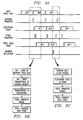
- the data input bus 14 transfers data for bit 1 (next to LSB) to the primary memory cell or data latch 16. This is seen on the first line of the timing diagram in Figure 2a. After the bit 1 is loaded into all of the respective respective memory cells, two control signals occur. First, shown on the second line of Figure 2a is the shadow transfer signal (22). This transfers the data from the primary memory cell to its secondary or shadow memory cell (18). For illustration, this is assumed to be a data latch, but could comprise any type of circuit that can store data and be cleared. This also transfers the data onto the electrodes or other activation circuitry of pixels 20a-20k (for a fanout of 11). The electrode state is shown on the third line of Figure 2a.
- the second control signal is the pixel transfer signal, shown on the fourth line of Figure 2a.
- the pixels then adjust to display bit 1 data in response to the pixel transfer signal, shown in the fourth line of Figure 2a.
- a flow chart process for the sequencing of the transfer signals and movement of the data at the area surrounded by the dashed line is shown in Figure 2b.
- Bit 0 is described as a clearable bit, which means that it's display time is less than the load time. For example, if bit 0, the LSB were cleared after its usual display time, and the next shadow transfer signal did not come for another LSB time, the load time of the device has effectively been doubled. Instead of having to load the device in 1/255th of a frame, the device could be loaded in 1/128th of a frame.
- multiplexed memory architecture keeps the costs of a system down, and allows high-speed operation. Additionally, using multiplexed memory architecture makes the average data rate approach or equal to the peak data rate, and therefore doesn't require expensive, high-speed processors. However, the limitation of multiplexed memory architecture is based upon its fanout being tied to a certain number of bits of intensity.
Landscapes
- Engineering & Computer Science (AREA)
- Physics & Mathematics (AREA)
- Computer Hardware Design (AREA)
- General Physics & Mathematics (AREA)
- Theoretical Computer Science (AREA)
- Control Of Indicators Other Than Cathode Ray Tubes (AREA)
- Mechanical Light Control Or Optical Switches (AREA)
- Liquid Crystal Display Device Control (AREA)
- Printers Or Recording Devices Using Electromagnetic And Radiation Means (AREA)
- Transforming Electric Information Into Light Information (AREA)
Applications Claiming Priority (2)
| Application Number | Priority Date | Filing Date | Title |
|---|---|---|---|
| US264387 | 1988-10-31 | ||
| US08/264,387 US5499062A (en) | 1994-06-23 | 1994-06-23 | Multiplexed memory timing with block reset and secondary memory |
Publications (2)
| Publication Number | Publication Date |
|---|---|
| EP0689181A1 true EP0689181A1 (de) | 1995-12-27 |
| EP0689181B1 EP0689181B1 (de) | 2000-01-05 |
Family
ID=23005842
Family Applications (1)
| Application Number | Title | Priority Date | Filing Date |
|---|---|---|---|
| EP95109828A Expired - Lifetime EP0689181B1 (de) | 1994-06-23 | 1995-06-23 | Speicherschaltungen für räumliche Lichtmodulatoren |
Country Status (7)
| Country | Link |
|---|---|
| US (1) | US5499062A (de) |
| EP (1) | EP0689181B1 (de) |
| JP (1) | JPH08201707A (de) |
| KR (1) | KR100346878B1 (de) |
| CN (1) | CN1072805C (de) |
| CA (1) | CA2149930A1 (de) |
| DE (1) | DE69514285T2 (de) |
Cited By (5)
| Publication number | Priority date | Publication date | Assignee | Title |
|---|---|---|---|---|
| EP0887786A3 (de) * | 1997-06-25 | 2000-07-05 | Sony Corporation | Anzeigegerät mit einem optischen räumlichen Modulator |
| WO2003060862A1 (en) * | 2002-01-18 | 2003-07-24 | Koninklijke Philips Electronics N.V. | Display device with picture decoding |
| US6600262B1 (en) | 1998-12-16 | 2003-07-29 | Sony Corporation | Field emission type cathode and electron emitting apparatus using piled platelike particles |
| EP3796300A1 (de) * | 2019-09-20 | 2021-03-24 | Beijing Xiaomi Mobile Software Co., Ltd. | Anzeigetafel, anzeigebildschirm und elektronische vorrichtung |
| US11676550B2 (en) | 2019-01-07 | 2023-06-13 | Sony Group Corporation | Spatial light modulator system, spatial light modulator device, and display apparatus for preventing influences of mechanical operations of a light modulation unit |
Families Citing this family (231)
| Publication number | Priority date | Publication date | Assignee | Title |
|---|---|---|---|---|
| US6219015B1 (en) | 1992-04-28 | 2001-04-17 | The Board Of Directors Of The Leland Stanford, Junior University | Method and apparatus for using an array of grating light valves to produce multicolor optical images |
| US6674562B1 (en) | 1994-05-05 | 2004-01-06 | Iridigm Display Corporation | Interferometric modulation of radiation |
| US8014059B2 (en) * | 1994-05-05 | 2011-09-06 | Qualcomm Mems Technologies, Inc. | System and method for charge control in a MEMS device |
| US7297471B1 (en) | 2003-04-15 | 2007-11-20 | Idc, Llc | Method for manufacturing an array of interferometric modulators |
| US7460291B2 (en) | 1994-05-05 | 2008-12-02 | Idc, Llc | Separable modulator |
| US7138984B1 (en) | 2001-06-05 | 2006-11-21 | Idc, Llc | Directly laminated touch sensitive screen |
| US7550794B2 (en) * | 2002-09-20 | 2009-06-23 | Idc, Llc | Micromechanical systems device comprising a displaceable electrode and a charge-trapping layer |
| US6680792B2 (en) * | 1994-05-05 | 2004-01-20 | Iridigm Display Corporation | Interferometric modulation of radiation |
| US7123216B1 (en) * | 1994-05-05 | 2006-10-17 | Idc, Llc | Photonic MEMS and structures |
| US5610624A (en) * | 1994-11-30 | 1997-03-11 | Texas Instruments Incorporated | Spatial light modulator with reduced possibility of an on state defect |
| US5757348A (en) | 1994-12-22 | 1998-05-26 | Displaytech, Inc. | Active matrix liquid crystal image generator with hybrid writing scheme |
| US5748164A (en) * | 1994-12-22 | 1998-05-05 | Displaytech, Inc. | Active matrix liquid crystal image generator |
| US5808800A (en) | 1994-12-22 | 1998-09-15 | Displaytech, Inc. | Optics arrangements including light source arrangements for an active matrix liquid crystal image generator |
| US5682174A (en) * | 1995-02-16 | 1997-10-28 | Texas Instruments Incorporated | Memory cell array for digital spatial light modulator |
| US5841579A (en) | 1995-06-07 | 1998-11-24 | Silicon Light Machines | Flat diffraction grating light valve |
| US6969635B2 (en) | 2000-12-07 | 2005-11-29 | Reflectivity, Inc. | Methods for depositing, releasing and packaging micro-electromechanical devices on wafer substrates |
| CA2187044C (en) * | 1995-10-06 | 2003-07-01 | Vishal Markandey | Method to reduce perceptual contouring in display systems |
| US7471444B2 (en) * | 1996-12-19 | 2008-12-30 | Idc, Llc | Interferometric modulation of radiation |
| US5982553A (en) | 1997-03-20 | 1999-11-09 | Silicon Light Machines | Display device incorporating one-dimensional grating light-valve array |
| US6088102A (en) | 1997-10-31 | 2000-07-11 | Silicon Light Machines | Display apparatus including grating light-valve array and interferometric optical system |
| WO1999052006A2 (en) | 1998-04-08 | 1999-10-14 | Etalon, Inc. | Interferometric modulation of radiation |
| US8928967B2 (en) | 1998-04-08 | 2015-01-06 | Qualcomm Mems Technologies, Inc. | Method and device for modulating light |
| US7532377B2 (en) | 1998-04-08 | 2009-05-12 | Idc, Llc | Movable micro-electromechanical device |
| US6339417B1 (en) | 1998-05-15 | 2002-01-15 | Inviso, Inc. | Display system having multiple memory elements per pixel |
| US6140983A (en) * | 1998-05-15 | 2000-10-31 | Inviso, Inc. | Display system having multiple memory elements per pixel with improved layout design |
| US6271808B1 (en) | 1998-06-05 | 2001-08-07 | Silicon Light Machines | Stereo head mounted display using a single display device |
| US6130770A (en) | 1998-06-23 | 2000-10-10 | Silicon Light Machines | Electron gun activated grating light valve |
| US6101036A (en) | 1998-06-23 | 2000-08-08 | Silicon Light Machines | Embossed diffraction grating alone and in combination with changeable image display |
| US6215579B1 (en) | 1998-06-24 | 2001-04-10 | Silicon Light Machines | Method and apparatus for modulating an incident light beam for forming a two-dimensional image |
| US6303986B1 (en) | 1998-07-29 | 2001-10-16 | Silicon Light Machines | Method of and apparatus for sealing an hermetic lid to a semiconductor die |
| US6872984B1 (en) | 1998-07-29 | 2005-03-29 | Silicon Light Machines Corporation | Method of sealing a hermetic lid to a semiconductor die at an angle |
| EP1600933A3 (de) * | 1998-08-03 | 2007-02-21 | Seiko Epson Corporation | Substrat für elektrooptische Vorrichtung, elektrooptische Vorrichtung, elektronisches Gerät, und Projektionsvideoanzeige |
| US6962419B2 (en) | 1998-09-24 | 2005-11-08 | Reflectivity, Inc | Micromirror elements, package for the micromirror elements, and projection system therefor |
| WO2003007049A1 (en) * | 1999-10-05 | 2003-01-23 | Iridigm Display Corporation | Photonic mems and structures |
| US6956878B1 (en) | 2000-02-07 | 2005-10-18 | Silicon Light Machines Corporation | Method and apparatus for reducing laser speckle using polarization averaging |
| US7300162B2 (en) | 2000-08-30 | 2007-11-27 | Texas Instruments Incorporated | Projection display |
| US6962771B1 (en) * | 2000-10-13 | 2005-11-08 | Taiwan Semiconductor Manufacturing Company, Ltd. | Dual damascene process |
| US7177081B2 (en) | 2001-03-08 | 2007-02-13 | Silicon Light Machines Corporation | High contrast grating light valve type device |
| US6707591B2 (en) | 2001-04-10 | 2004-03-16 | Silicon Light Machines | Angled illumination for a single order light modulator based projection system |
| US6865346B1 (en) | 2001-06-05 | 2005-03-08 | Silicon Light Machines Corporation | Fiber optic transceiver |
| US6782205B2 (en) | 2001-06-25 | 2004-08-24 | Silicon Light Machines | Method and apparatus for dynamic equalization in wavelength division multiplexing |
| US6747781B2 (en) | 2001-06-25 | 2004-06-08 | Silicon Light Machines, Inc. | Method, apparatus, and diffuser for reducing laser speckle |
| US6589625B1 (en) | 2001-08-01 | 2003-07-08 | Iridigm Display Corporation | Hermetic seal and method to create the same |
| US6829092B2 (en) | 2001-08-15 | 2004-12-07 | Silicon Light Machines, Inc. | Blazed grating light valve |
| US6930364B2 (en) | 2001-09-13 | 2005-08-16 | Silicon Light Machines Corporation | Microelectronic mechanical system and methods |
| US6956995B1 (en) | 2001-11-09 | 2005-10-18 | Silicon Light Machines Corporation | Optical communication arrangement |
| US6800238B1 (en) | 2002-01-15 | 2004-10-05 | Silicon Light Machines, Inc. | Method for domain patterning in low coercive field ferroelectrics |
| US6794119B2 (en) * | 2002-02-12 | 2004-09-21 | Iridigm Display Corporation | Method for fabricating a structure for a microelectromechanical systems (MEMS) device |
| US6574033B1 (en) | 2002-02-27 | 2003-06-03 | Iridigm Display Corporation | Microelectromechanical systems device and method for fabricating same |
| US6767751B2 (en) | 2002-05-28 | 2004-07-27 | Silicon Light Machines, Inc. | Integrated driver process flow |
| US6728023B1 (en) | 2002-05-28 | 2004-04-27 | Silicon Light Machines | Optical device arrays with optimized image resolution |
| US7054515B1 (en) | 2002-05-30 | 2006-05-30 | Silicon Light Machines Corporation | Diffractive light modulator-based dynamic equalizer with integrated spectral monitor |
| US6822797B1 (en) | 2002-05-31 | 2004-11-23 | Silicon Light Machines, Inc. | Light modulator structure for producing high-contrast operation using zero-order light |
| US7061512B2 (en) * | 2002-06-11 | 2006-06-13 | Texas Instruments Incorporated | Constant-weight bit-slice PWM method and system for scrolling color display systems |
| US6829258B1 (en) | 2002-06-26 | 2004-12-07 | Silicon Light Machines, Inc. | Rapidly tunable external cavity laser |
| US6714337B1 (en) | 2002-06-28 | 2004-03-30 | Silicon Light Machines | Method and device for modulating a light beam and having an improved gamma response |
| US6813059B2 (en) | 2002-06-28 | 2004-11-02 | Silicon Light Machines, Inc. | Reduced formation of asperities in contact micro-structures |
| US6908201B2 (en) | 2002-06-28 | 2005-06-21 | Silicon Light Machines Corporation | Micro-support structures |
| US7057795B2 (en) | 2002-08-20 | 2006-06-06 | Silicon Light Machines Corporation | Micro-structures with individually addressable ribbon pairs |
| US6801354B1 (en) | 2002-08-20 | 2004-10-05 | Silicon Light Machines, Inc. | 2-D diffraction grating for substantially eliminating polarization dependent losses |
| US7781850B2 (en) * | 2002-09-20 | 2010-08-24 | Qualcomm Mems Technologies, Inc. | Controlling electromechanical behavior of structures within a microelectromechanical systems device |
| US6712480B1 (en) | 2002-09-27 | 2004-03-30 | Silicon Light Machines | Controlled curvature of stressed micro-structures |
| US6928207B1 (en) | 2002-12-12 | 2005-08-09 | Silicon Light Machines Corporation | Apparatus for selectively blocking WDM channels |
| US7057819B1 (en) | 2002-12-17 | 2006-06-06 | Silicon Light Machines Corporation | High contrast tilting ribbon blazed grating |
| US6987600B1 (en) | 2002-12-17 | 2006-01-17 | Silicon Light Machines Corporation | Arbitrary phase profile for better equalization in dynamic gain equalizer |
| US6934070B1 (en) | 2002-12-18 | 2005-08-23 | Silicon Light Machines Corporation | Chirped optical MEM device |
| US6927891B1 (en) | 2002-12-23 | 2005-08-09 | Silicon Light Machines Corporation | Tilt-able grating plane for improved crosstalk in 1×N blaze switches |
| US7068372B1 (en) | 2003-01-28 | 2006-06-27 | Silicon Light Machines Corporation | MEMS interferometer-based reconfigurable optical add-and-drop multiplexor |
| TW200413810A (en) | 2003-01-29 | 2004-08-01 | Prime View Int Co Ltd | Light interference display panel and its manufacturing method |
| US7286764B1 (en) | 2003-02-03 | 2007-10-23 | Silicon Light Machines Corporation | Reconfigurable modulator-based optical add-and-drop multiplexer |
| US6947613B1 (en) | 2003-02-11 | 2005-09-20 | Silicon Light Machines Corporation | Wavelength selective switch and equalizer |
| US7042622B2 (en) | 2003-10-30 | 2006-05-09 | Reflectivity, Inc | Micromirror and post arrangements on substrates |
| US6922272B1 (en) | 2003-02-14 | 2005-07-26 | Silicon Light Machines Corporation | Method and apparatus for leveling thermal stress variations in multi-layer MEMS devices |
| US6829077B1 (en) | 2003-02-28 | 2004-12-07 | Silicon Light Machines, Inc. | Diffractive light modulator with dynamically rotatable diffraction plane |
| US7391973B1 (en) | 2003-02-28 | 2008-06-24 | Silicon Light Machines Corporation | Two-stage gain equalizer |
| US6806997B1 (en) | 2003-02-28 | 2004-10-19 | Silicon Light Machines, Inc. | Patterned diffractive light modulator ribbon for PDL reduction |
| US6922273B1 (en) | 2003-02-28 | 2005-07-26 | Silicon Light Machines Corporation | PDL mitigation structure for diffractive MEMS and gratings |
| US7027202B1 (en) | 2003-02-28 | 2006-04-11 | Silicon Light Machines Corp | Silicon substrate as a light modulator sacrificial layer |
| US7042611B1 (en) | 2003-03-03 | 2006-05-09 | Silicon Light Machines Corporation | Pre-deflected bias ribbons |
| TW594360B (en) * | 2003-04-21 | 2004-06-21 | Prime View Int Corp Ltd | A method for fabricating an interference display cell |
| CN1860520B (zh) | 2003-05-20 | 2011-07-06 | 辛迪安特公司 | 数字底板 |
| TW570896B (en) | 2003-05-26 | 2004-01-11 | Prime View Int Co Ltd | A method for fabricating an interference display cell |
| US7221495B2 (en) * | 2003-06-24 | 2007-05-22 | Idc Llc | Thin film precursor stack for MEMS manufacturing |
| TW200506479A (en) * | 2003-08-15 | 2005-02-16 | Prime View Int Co Ltd | Color changeable pixel for an interference display |
| TWI231865B (en) * | 2003-08-26 | 2005-05-01 | Prime View Int Co Ltd | An interference display cell and fabrication method thereof |
| TWI232333B (en) * | 2003-09-03 | 2005-05-11 | Prime View Int Co Ltd | Display unit using interferometric modulation and manufacturing method thereof |
| TW593126B (en) | 2003-09-30 | 2004-06-21 | Prime View Int Co Ltd | A structure of a micro electro mechanical system and manufacturing the same |
| US7012726B1 (en) | 2003-11-03 | 2006-03-14 | Idc, Llc | MEMS devices with unreleased thin film components |
| US7161728B2 (en) | 2003-12-09 | 2007-01-09 | Idc, Llc | Area array modulation and lead reduction in interferometric modulators |
| US7142346B2 (en) | 2003-12-09 | 2006-11-28 | Idc, Llc | System and method for addressing a MEMS display |
| US7532194B2 (en) * | 2004-02-03 | 2009-05-12 | Idc, Llc | Driver voltage adjuster |
| US7119945B2 (en) | 2004-03-03 | 2006-10-10 | Idc, Llc | Altering temporal response of microelectromechanical elements |
| US7706050B2 (en) * | 2004-03-05 | 2010-04-27 | Qualcomm Mems Technologies, Inc. | Integrated modulator illumination |
| US7720148B2 (en) * | 2004-03-26 | 2010-05-18 | The Hong Kong University Of Science And Technology | Efficient multi-frame motion estimation for video compression |
| US7060895B2 (en) * | 2004-05-04 | 2006-06-13 | Idc, Llc | Modifying the electro-mechanical behavior of devices |
| US7476327B2 (en) * | 2004-05-04 | 2009-01-13 | Idc, Llc | Method of manufacture for microelectromechanical devices |
| US7164520B2 (en) * | 2004-05-12 | 2007-01-16 | Idc, Llc | Packaging for an interferometric modulator |
| US7256922B2 (en) * | 2004-07-02 | 2007-08-14 | Idc, Llc | Interferometric modulators with thin film transistors |
| TWI233916B (en) * | 2004-07-09 | 2005-06-11 | Prime View Int Co Ltd | A structure of a micro electro mechanical system |
| KR101313117B1 (ko) * | 2004-07-29 | 2013-09-30 | 퀄컴 엠이엠에스 테크놀로지스, 인크. | 간섭 변조기의 미소기전 동작을 위한 시스템 및 방법 |
| US7551159B2 (en) | 2004-08-27 | 2009-06-23 | Idc, Llc | System and method of sensing actuation and release voltages of an interferometric modulator |
| US7560299B2 (en) * | 2004-08-27 | 2009-07-14 | Idc, Llc | Systems and methods of actuating MEMS display elements |
| US7889163B2 (en) * | 2004-08-27 | 2011-02-15 | Qualcomm Mems Technologies, Inc. | Drive method for MEMS devices |
| US7499208B2 (en) | 2004-08-27 | 2009-03-03 | Udc, Llc | Current mode display driver circuit realization feature |
| US7515147B2 (en) * | 2004-08-27 | 2009-04-07 | Idc, Llc | Staggered column drive circuit systems and methods |
| US7602375B2 (en) * | 2004-09-27 | 2009-10-13 | Idc, Llc | Method and system for writing data to MEMS display elements |
| US7527995B2 (en) * | 2004-09-27 | 2009-05-05 | Qualcomm Mems Technologies, Inc. | Method of making prestructure for MEMS systems |
| US7317568B2 (en) * | 2004-09-27 | 2008-01-08 | Idc, Llc | System and method of implementation of interferometric modulators for display mirrors |
| US7299681B2 (en) * | 2004-09-27 | 2007-11-27 | Idc, Llc | Method and system for detecting leak in electronic devices |
| US7813026B2 (en) * | 2004-09-27 | 2010-10-12 | Qualcomm Mems Technologies, Inc. | System and method of reducing color shift in a display |
| US7553684B2 (en) * | 2004-09-27 | 2009-06-30 | Idc, Llc | Method of fabricating interferometric devices using lift-off processing techniques |
| US7692839B2 (en) * | 2004-09-27 | 2010-04-06 | Qualcomm Mems Technologies, Inc. | System and method of providing MEMS device with anti-stiction coating |
| US7460246B2 (en) * | 2004-09-27 | 2008-12-02 | Idc, Llc | Method and system for sensing light using interferometric elements |
| US8310441B2 (en) | 2004-09-27 | 2012-11-13 | Qualcomm Mems Technologies, Inc. | Method and system for writing data to MEMS display elements |
| US7321456B2 (en) * | 2004-09-27 | 2008-01-22 | Idc, Llc | Method and device for corner interferometric modulation |
| US7302157B2 (en) * | 2004-09-27 | 2007-11-27 | Idc, Llc | System and method for multi-level brightness in interferometric modulation |
| US7369296B2 (en) * | 2004-09-27 | 2008-05-06 | Idc, Llc | Device and method for modifying actuation voltage thresholds of a deformable membrane in an interferometric modulator |
| US20060076634A1 (en) | 2004-09-27 | 2006-04-13 | Lauren Palmateer | Method and system for packaging MEMS devices with incorporated getter |
| WO2006037044A1 (en) * | 2004-09-27 | 2006-04-06 | Idc, Llc | Method and device for multistate interferometric light modulation |
| US7359066B2 (en) * | 2004-09-27 | 2008-04-15 | Idc, Llc | Electro-optical measurement of hysteresis in interferometric modulators |
| US7446927B2 (en) * | 2004-09-27 | 2008-11-04 | Idc, Llc | MEMS switch with set and latch electrodes |
| US7583429B2 (en) | 2004-09-27 | 2009-09-01 | Idc, Llc | Ornamental display device |
| US7343080B2 (en) | 2004-09-27 | 2008-03-11 | Idc, Llc | System and method of testing humidity in a sealed MEMS device |
| US7429334B2 (en) * | 2004-09-27 | 2008-09-30 | Idc, Llc | Methods of fabricating interferometric modulators by selectively removing a material |
| US20060077126A1 (en) * | 2004-09-27 | 2006-04-13 | Manish Kothari | Apparatus and method for arranging devices into an interconnected array |
| US7259449B2 (en) * | 2004-09-27 | 2007-08-21 | Idc, Llc | Method and system for sealing a substrate |
| US7373026B2 (en) * | 2004-09-27 | 2008-05-13 | Idc, Llc | MEMS device fabricated on a pre-patterned substrate |
| US7355780B2 (en) | 2004-09-27 | 2008-04-08 | Idc, Llc | System and method of illuminating interferometric modulators using backlighting |
| US7369294B2 (en) * | 2004-09-27 | 2008-05-06 | Idc, Llc | Ornamental display device |
| US7719500B2 (en) * | 2004-09-27 | 2010-05-18 | Qualcomm Mems Technologies, Inc. | Reflective display pixels arranged in non-rectangular arrays |
| US7710629B2 (en) * | 2004-09-27 | 2010-05-04 | Qualcomm Mems Technologies, Inc. | System and method for display device with reinforcing substance |
| US7936497B2 (en) * | 2004-09-27 | 2011-05-03 | Qualcomm Mems Technologies, Inc. | MEMS device having deformable membrane characterized by mechanical persistence |
| US7545550B2 (en) * | 2004-09-27 | 2009-06-09 | Idc, Llc | Systems and methods of actuating MEMS display elements |
| US7327510B2 (en) | 2004-09-27 | 2008-02-05 | Idc, Llc | Process for modifying offset voltage characteristics of an interferometric modulator |
| US8878825B2 (en) | 2004-09-27 | 2014-11-04 | Qualcomm Mems Technologies, Inc. | System and method for providing a variable refresh rate of an interferometric modulator display |
| US7417783B2 (en) * | 2004-09-27 | 2008-08-26 | Idc, Llc | Mirror and mirror layer for optical modulator and method |
| US7368803B2 (en) * | 2004-09-27 | 2008-05-06 | Idc, Llc | System and method for protecting microelectromechanical systems array using back-plate with non-flat portion |
| US20060176487A1 (en) * | 2004-09-27 | 2006-08-10 | William Cummings | Process control monitors for interferometric modulators |
| US7679627B2 (en) | 2004-09-27 | 2010-03-16 | Qualcomm Mems Technologies, Inc. | Controller and driver features for bi-stable display |
| US7136213B2 (en) * | 2004-09-27 | 2006-11-14 | Idc, Llc | Interferometric modulators having charge persistence |
| US7535466B2 (en) * | 2004-09-27 | 2009-05-19 | Idc, Llc | System with server based control of client device display features |
| US7345805B2 (en) * | 2004-09-27 | 2008-03-18 | Idc, Llc | Interferometric modulator array with integrated MEMS electrical switches |
| US7668415B2 (en) * | 2004-09-27 | 2010-02-23 | Qualcomm Mems Technologies, Inc. | Method and device for providing electronic circuitry on a backplate |
| US7893919B2 (en) | 2004-09-27 | 2011-02-22 | Qualcomm Mems Technologies, Inc. | Display region architectures |
| US7289256B2 (en) * | 2004-09-27 | 2007-10-30 | Idc, Llc | Electrical characterization of interferometric modulators |
| US7532195B2 (en) * | 2004-09-27 | 2009-05-12 | Idc, Llc | Method and system for reducing power consumption in a display |
| US7372613B2 (en) | 2004-09-27 | 2008-05-13 | Idc, Llc | Method and device for multistate interferometric light modulation |
| US7405924B2 (en) | 2004-09-27 | 2008-07-29 | Idc, Llc | System and method for protecting microelectromechanical systems array using structurally reinforced back-plate |
| US7289259B2 (en) * | 2004-09-27 | 2007-10-30 | Idc, Llc | Conductive bus structure for interferometric modulator array |
| US7808703B2 (en) * | 2004-09-27 | 2010-10-05 | Qualcomm Mems Technologies, Inc. | System and method for implementation of interferometric modulator displays |
| US20060066596A1 (en) * | 2004-09-27 | 2006-03-30 | Sampsell Jeffrey B | System and method of transmitting video data |
| US8124434B2 (en) * | 2004-09-27 | 2012-02-28 | Qualcomm Mems Technologies, Inc. | Method and system for packaging a display |
| US7453579B2 (en) | 2004-09-27 | 2008-11-18 | Idc, Llc | Measurement of the dynamic characteristics of interferometric modulators |
| US7920135B2 (en) * | 2004-09-27 | 2011-04-05 | Qualcomm Mems Technologies, Inc. | Method and system for driving a bi-stable display |
| US20060065366A1 (en) * | 2004-09-27 | 2006-03-30 | Cummings William J | Portable etch chamber |
| US20060065622A1 (en) * | 2004-09-27 | 2006-03-30 | Floyd Philip D | Method and system for xenon fluoride etching with enhanced efficiency |
| US8008736B2 (en) * | 2004-09-27 | 2011-08-30 | Qualcomm Mems Technologies, Inc. | Analog interferometric modulator device |
| US7130104B2 (en) * | 2004-09-27 | 2006-10-31 | Idc, Llc | Methods and devices for inhibiting tilting of a mirror in an interferometric modulator |
| US7916103B2 (en) | 2004-09-27 | 2011-03-29 | Qualcomm Mems Technologies, Inc. | System and method for display device with end-of-life phenomena |
| US7424198B2 (en) * | 2004-09-27 | 2008-09-09 | Idc, Llc | Method and device for packaging a substrate |
| US7843410B2 (en) * | 2004-09-27 | 2010-11-30 | Qualcomm Mems Technologies, Inc. | Method and device for electrically programmable display |
| US7724993B2 (en) * | 2004-09-27 | 2010-05-25 | Qualcomm Mems Technologies, Inc. | MEMS switches with deforming membranes |
| US7701631B2 (en) * | 2004-09-27 | 2010-04-20 | Qualcomm Mems Technologies, Inc. | Device having patterned spacers for backplates and method of making the same |
| US20060066594A1 (en) * | 2004-09-27 | 2006-03-30 | Karen Tyger | Systems and methods for driving a bi-stable display element |
| US7684104B2 (en) * | 2004-09-27 | 2010-03-23 | Idc, Llc | MEMS using filler material and method |
| US7630119B2 (en) * | 2004-09-27 | 2009-12-08 | Qualcomm Mems Technologies, Inc. | Apparatus and method for reducing slippage between structures in an interferometric modulator |
| US7420725B2 (en) | 2004-09-27 | 2008-09-02 | Idc, Llc | Device having a conductive light absorbing mask and method for fabricating same |
| US7310179B2 (en) | 2004-09-27 | 2007-12-18 | Idc, Llc | Method and device for selective adjustment of hysteresis window |
| US7944599B2 (en) | 2004-09-27 | 2011-05-17 | Qualcomm Mems Technologies, Inc. | Electromechanical device with optical function separated from mechanical and electrical function |
| US7564612B2 (en) * | 2004-09-27 | 2009-07-21 | Idc, Llc | Photonic MEMS and structures |
| US7586484B2 (en) * | 2004-09-27 | 2009-09-08 | Idc, Llc | Controller and driver features for bi-stable display |
| US20060067650A1 (en) * | 2004-09-27 | 2006-03-30 | Clarence Chui | Method of making a reflective display device using thin film transistor production techniques |
| US7415186B2 (en) * | 2004-09-27 | 2008-08-19 | Idc, Llc | Methods for visually inspecting interferometric modulators for defects |
| US20060103643A1 (en) * | 2004-09-27 | 2006-05-18 | Mithran Mathew | Measuring and modeling power consumption in displays |
| US7492502B2 (en) * | 2004-09-27 | 2009-02-17 | Idc, Llc | Method of fabricating a free-standing microstructure |
| US7304784B2 (en) * | 2004-09-27 | 2007-12-04 | Idc, Llc | Reflective display device having viewable display on both sides |
| US7161730B2 (en) | 2004-09-27 | 2007-01-09 | Idc, Llc | System and method for providing thermal compensation for an interferometric modulator display |
| US7417735B2 (en) * | 2004-09-27 | 2008-08-26 | Idc, Llc | Systems and methods for measuring color and contrast in specular reflective devices |
| US7653371B2 (en) * | 2004-09-27 | 2010-01-26 | Qualcomm Mems Technologies, Inc. | Selectable capacitance circuit |
| US7675669B2 (en) | 2004-09-27 | 2010-03-09 | Qualcomm Mems Technologies, Inc. | Method and system for driving interferometric modulators |
| US7554714B2 (en) * | 2004-09-27 | 2009-06-30 | Idc, Llc | Device and method for manipulation of thermal response in a modulator |
| US7349136B2 (en) * | 2004-09-27 | 2008-03-25 | Idc, Llc | Method and device for a display having transparent components integrated therein |
| US7405861B2 (en) * | 2004-09-27 | 2008-07-29 | Idc, Llc | Method and device for protecting interferometric modulators from electrostatic discharge |
| US7626581B2 (en) * | 2004-09-27 | 2009-12-01 | Idc, Llc | Device and method for display memory using manipulation of mechanical response |
| TW200628877A (en) * | 2005-02-04 | 2006-08-16 | Prime View Int Co Ltd | Method of manufacturing optical interference type color display |
| US7920136B2 (en) * | 2005-05-05 | 2011-04-05 | Qualcomm Mems Technologies, Inc. | System and method of driving a MEMS display device |
| KR20080027236A (ko) | 2005-05-05 | 2008-03-26 | 콸콤 인코포레이티드 | 다이나믹 드라이버 ic 및 디스플레이 패널 구성 |
| US7948457B2 (en) * | 2005-05-05 | 2011-05-24 | Qualcomm Mems Technologies, Inc. | Systems and methods of actuating MEMS display elements |
| US20060277486A1 (en) * | 2005-06-02 | 2006-12-07 | Skinner David N | File or user interface element marking system |
| WO2007013939A1 (en) * | 2005-07-22 | 2007-02-01 | Qualcomm Incorporated | Support structure for mems device and methods therefor |
| US7355779B2 (en) * | 2005-09-02 | 2008-04-08 | Idc, Llc | Method and system for driving MEMS display elements |
| US7630114B2 (en) * | 2005-10-28 | 2009-12-08 | Idc, Llc | Diffusion barrier layer for MEMS devices |
| US8391630B2 (en) * | 2005-12-22 | 2013-03-05 | Qualcomm Mems Technologies, Inc. | System and method for power reduction when decompressing video streams for interferometric modulator displays |
| US7795061B2 (en) | 2005-12-29 | 2010-09-14 | Qualcomm Mems Technologies, Inc. | Method of creating MEMS device cavities by a non-etching process |
| US7636151B2 (en) * | 2006-01-06 | 2009-12-22 | Qualcomm Mems Technologies, Inc. | System and method for providing residual stress test structures |
| US7916980B2 (en) | 2006-01-13 | 2011-03-29 | Qualcomm Mems Technologies, Inc. | Interconnect structure for MEMS device |
| US7382515B2 (en) * | 2006-01-18 | 2008-06-03 | Qualcomm Mems Technologies, Inc. | Silicon-rich silicon nitrides as etch stops in MEMS manufacture |
| US8194056B2 (en) * | 2006-02-09 | 2012-06-05 | Qualcomm Mems Technologies Inc. | Method and system for writing data to MEMS display elements |
| US7582952B2 (en) * | 2006-02-21 | 2009-09-01 | Qualcomm Mems Technologies, Inc. | Method for providing and removing discharging interconnect for chip-on-glass output leads and structures thereof |
| US7547568B2 (en) * | 2006-02-22 | 2009-06-16 | Qualcomm Mems Technologies, Inc. | Electrical conditioning of MEMS device and insulating layer thereof |
| US7550810B2 (en) * | 2006-02-23 | 2009-06-23 | Qualcomm Mems Technologies, Inc. | MEMS device having a layer movable at asymmetric rates |
| US7450295B2 (en) * | 2006-03-02 | 2008-11-11 | Qualcomm Mems Technologies, Inc. | Methods for producing MEMS with protective coatings using multi-component sacrificial layers |
| US7643203B2 (en) | 2006-04-10 | 2010-01-05 | Qualcomm Mems Technologies, Inc. | Interferometric optical display system with broadband characteristics |
| US7903047B2 (en) * | 2006-04-17 | 2011-03-08 | Qualcomm Mems Technologies, Inc. | Mode indicator for interferometric modulator displays |
| US7417784B2 (en) * | 2006-04-19 | 2008-08-26 | Qualcomm Mems Technologies, Inc. | Microelectromechanical device and method utilizing a porous surface |
| US7623287B2 (en) * | 2006-04-19 | 2009-11-24 | Qualcomm Mems Technologies, Inc. | Non-planar surface structures and process for microelectromechanical systems |
| US7711239B2 (en) | 2006-04-19 | 2010-05-04 | Qualcomm Mems Technologies, Inc. | Microelectromechanical device and method utilizing nanoparticles |
| US7527996B2 (en) * | 2006-04-19 | 2009-05-05 | Qualcomm Mems Technologies, Inc. | Non-planar surface structures and process for microelectromechanical systems |
| US20070249078A1 (en) * | 2006-04-19 | 2007-10-25 | Ming-Hau Tung | Non-planar surface structures and process for microelectromechanical systems |
| US8049713B2 (en) * | 2006-04-24 | 2011-11-01 | Qualcomm Mems Technologies, Inc. | Power consumption optimized display update |
| US7369292B2 (en) * | 2006-05-03 | 2008-05-06 | Qualcomm Mems Technologies, Inc. | Electrode and interconnect materials for MEMS devices |
| US7321457B2 (en) | 2006-06-01 | 2008-01-22 | Qualcomm Incorporated | Process and structure for fabrication of MEMS device having isolated edge posts |
| US7649671B2 (en) * | 2006-06-01 | 2010-01-19 | Qualcomm Mems Technologies, Inc. | Analog interferometric modulator device with electrostatic actuation and release |
| US7405863B2 (en) * | 2006-06-01 | 2008-07-29 | Qualcomm Mems Technologies, Inc. | Patterning of mechanical layer in MEMS to reduce stresses at supports |
| US7471442B2 (en) * | 2006-06-15 | 2008-12-30 | Qualcomm Mems Technologies, Inc. | Method and apparatus for low range bit depth enhancements for MEMS display architectures |
| US7702192B2 (en) | 2006-06-21 | 2010-04-20 | Qualcomm Mems Technologies, Inc. | Systems and methods for driving MEMS display |
| US7385744B2 (en) * | 2006-06-28 | 2008-06-10 | Qualcomm Mems Technologies, Inc. | Support structure for free-standing MEMS device and methods for forming the same |
| US7835061B2 (en) * | 2006-06-28 | 2010-11-16 | Qualcomm Mems Technologies, Inc. | Support structures for free-standing electromechanical devices |
| US7777715B2 (en) | 2006-06-29 | 2010-08-17 | Qualcomm Mems Technologies, Inc. | Passive circuits for de-multiplexing display inputs |
| US7527998B2 (en) | 2006-06-30 | 2009-05-05 | Qualcomm Mems Technologies, Inc. | Method of manufacturing MEMS devices providing air gap control |
| US7388704B2 (en) * | 2006-06-30 | 2008-06-17 | Qualcomm Mems Technologies, Inc. | Determination of interferometric modulator mirror curvature and airgap variation using digital photographs |
| US7763546B2 (en) | 2006-08-02 | 2010-07-27 | Qualcomm Mems Technologies, Inc. | Methods for reducing surface charges during the manufacture of microelectromechanical systems devices |
| US7566664B2 (en) * | 2006-08-02 | 2009-07-28 | Qualcomm Mems Technologies, Inc. | Selective etching of MEMS using gaseous halides and reactive co-etchants |
| US20080043315A1 (en) * | 2006-08-15 | 2008-02-21 | Cummings William J | High profile contacts for microelectromechanical systems |
| US7719752B2 (en) | 2007-05-11 | 2010-05-18 | Qualcomm Mems Technologies, Inc. | MEMS structures, methods of fabricating MEMS components on separate substrates and assembly of same |
| KR20100121498A (ko) * | 2008-02-11 | 2010-11-17 | 퀄컴 엠이엠스 테크놀로지스, 인크. | 디스플레이 구동 체계가 통합된 표시소자의 감지, 측정 혹은 평가 방법 및 장치, 그리고 이를 이용한 시스템 및 용도 |
| US8736590B2 (en) * | 2009-03-27 | 2014-05-27 | Qualcomm Mems Technologies, Inc. | Low voltage driver scheme for interferometric modulators |
| TWI493959B (zh) * | 2009-05-07 | 2015-07-21 | Mstar Semiconductor Inc | 影像處理系統及影像處理方法 |
| JP2013524287A (ja) | 2010-04-09 | 2013-06-17 | クォルコム・メムズ・テクノロジーズ・インコーポレーテッド | 電気機械デバイスの機械層及びその形成方法 |
| US9134527B2 (en) | 2011-04-04 | 2015-09-15 | Qualcomm Mems Technologies, Inc. | Pixel via and methods of forming the same |
| US8963159B2 (en) | 2011-04-04 | 2015-02-24 | Qualcomm Mems Technologies, Inc. | Pixel via and methods of forming the same |
Citations (3)
| Publication number | Priority date | Publication date | Assignee | Title |
|---|---|---|---|---|
| WO1992012506A1 (en) * | 1991-01-04 | 1992-07-23 | Rank Brimar Limited | Display device |
| US5278652A (en) | 1991-04-01 | 1994-01-11 | Texas Instruments Incorporated | DMD architecture and timing for use in a pulse width modulated display system |
| EP0610665A1 (de) | 1993-01-11 | 1994-08-17 | Texas Instruments Incorporated | Pixelkontrollschaltung für räumlichen Lichtmodulator |
Family Cites Families (3)
| Publication number | Priority date | Publication date | Assignee | Title |
|---|---|---|---|---|
| US4039890A (en) * | 1974-08-16 | 1977-08-02 | Monsanto Company | Integrated semiconductor light-emitting display array |
| US4495492A (en) * | 1982-05-05 | 1985-01-22 | Litton Systems, Inc. | Magneto-optic chip with gray-scale capability |
| US4638309A (en) * | 1983-09-08 | 1987-01-20 | Texas Instruments Incorporated | Spatial light modulator drive system |
-
1994
- 1994-06-23 US US08/264,387 patent/US5499062A/en not_active Expired - Lifetime
-
1995
- 1995-05-23 CA CA002149930A patent/CA2149930A1/en not_active Abandoned
- 1995-06-22 KR KR1019950016839A patent/KR100346878B1/ko not_active Expired - Lifetime
- 1995-06-23 DE DE69514285T patent/DE69514285T2/de not_active Expired - Lifetime
- 1995-06-23 EP EP95109828A patent/EP0689181B1/de not_active Expired - Lifetime
- 1995-06-23 JP JP15788095A patent/JPH08201707A/ja active Pending
- 1995-06-23 CN CN95108041A patent/CN1072805C/zh not_active Expired - Fee Related
Patent Citations (3)
| Publication number | Priority date | Publication date | Assignee | Title |
|---|---|---|---|---|
| WO1992012506A1 (en) * | 1991-01-04 | 1992-07-23 | Rank Brimar Limited | Display device |
| US5278652A (en) | 1991-04-01 | 1994-01-11 | Texas Instruments Incorporated | DMD architecture and timing for use in a pulse width modulated display system |
| EP0610665A1 (de) | 1993-01-11 | 1994-08-17 | Texas Instruments Incorporated | Pixelkontrollschaltung für räumlichen Lichtmodulator |
Non-Patent Citations (1)
| Title |
|---|
| J. WAHL, T. MATUSZCZYK: "Experimental driver and addressing techniques for ferroelectric liquid crystal display devices", JOURNAL OF PHYSICS E SCIENTIFIC INSTRUMENTS., vol. 21, no. 5, BRISTOL GB, pages 460 - 466, XP000073241 * |
Cited By (6)
| Publication number | Priority date | Publication date | Assignee | Title |
|---|---|---|---|---|
| EP0887786A3 (de) * | 1997-06-25 | 2000-07-05 | Sony Corporation | Anzeigegerät mit einem optischen räumlichen Modulator |
| US6600262B1 (en) | 1998-12-16 | 2003-07-29 | Sony Corporation | Field emission type cathode and electron emitting apparatus using piled platelike particles |
| WO2003060862A1 (en) * | 2002-01-18 | 2003-07-24 | Koninklijke Philips Electronics N.V. | Display device with picture decoding |
| US11676550B2 (en) | 2019-01-07 | 2023-06-13 | Sony Group Corporation | Spatial light modulator system, spatial light modulator device, and display apparatus for preventing influences of mechanical operations of a light modulation unit |
| EP3796300A1 (de) * | 2019-09-20 | 2021-03-24 | Beijing Xiaomi Mobile Software Co., Ltd. | Anzeigetafel, anzeigebildschirm und elektronische vorrichtung |
| US11100865B2 (en) | 2019-09-20 | 2021-08-24 | Beijing Xiaomi Mobile Software Co., Ltd. | Display panel, display screen and electronic device |
Also Published As
| Publication number | Publication date |
|---|---|
| KR100346878B1 (ko) | 2002-11-07 |
| DE69514285T2 (de) | 2000-08-10 |
| JPH08201707A (ja) | 1996-08-09 |
| CN1120678A (zh) | 1996-04-17 |
| EP0689181B1 (de) | 2000-01-05 |
| DE69514285D1 (de) | 2000-02-10 |
| CA2149930A1 (en) | 1995-12-24 |
| US5499062A (en) | 1996-03-12 |
| CN1072805C (zh) | 2001-10-10 |
Similar Documents
| Publication | Publication Date | Title |
|---|---|---|
| US5499062A (en) | Multiplexed memory timing with block reset and secondary memory | |
| KR100346877B1 (ko) | 디지탈비디오시스템에서순간아티팩트를감소시키는방법및시스템 | |
| US6201521B1 (en) | Divided reset for addressing spatial light modulator | |
| US5619228A (en) | Method for reducing temporal artifacts in digital video systems | |
| US5548301A (en) | Pixel control circuitry for spatial light modulator | |
| EP0845771B1 (de) | Verfahren zum Steuern der Laden/Rückstellung-Sequenz für räumlichen Lichtmodulatoren | |
| US5497172A (en) | Pulse width modulation for spatial light modulator with split reset addressing | |
| US6480177B2 (en) | Blocked stepped address voltage for micromechanical devices | |
| KR100459053B1 (ko) | 영상디스플레이시스템에서아티팩트의제거방법 | |
| EP0513551B1 (de) | Bildanzeigevorrichtung | |
| EP0655858B1 (de) | Graustufendruck mit Verwendung von räumlichen Lichtmodulatoren | |
| US7317464B2 (en) | Pulse width modulated spatial light modulators with offset pulses | |
| US6462728B1 (en) | Apparatus having a DAC-controlled ramp generator for applying voltages to individual pixels in a color electro-optic display device | |
| US20030142274A1 (en) | Dmd-based image display systems | |
| EP0689345A2 (de) | Struktur von DMDs und Ablaufsteuerung zur Anwendung in einem Anzeigesystem mit Pulsbreitenmodulation | |
| EP0557360A1 (de) | Verfahren und einrichtung zum steuern von verformbaren spiegeln. | |
| US6719427B2 (en) | Display device, projection display apparatus, driving device for light modulator, and method for driving light modulator | |
| KR100413310B1 (ko) | 픽셀데이타디스플레이방법 | |
| JP3790277B2 (ja) | パルス幅変調ディジタル表示画素の強度調節方法及びこの方法を適用される表示システム | |
| WO1986007650A1 (en) | Method and apparatus for generating multi-color displays | |
| EP0504816A1 (de) | Verfahren zum Erzielen von Grautönen und hoher Bildfrequenz in einem Flüssigkristalldisplay mit steiler elektrooptischer Charakteristik | |
| EP0919982A1 (de) | Flüssigkristallanzeigesteuergerät mit Unterrahmen-Steuerung | |
| KR20030052559A (ko) | 데이터 비트분리형 디지털 구동 방식의 lcos 프로젝터시스템 |
Legal Events
| Date | Code | Title | Description |
|---|---|---|---|
| PUAI | Public reference made under article 153(3) epc to a published international application that has entered the european phase |
Free format text: ORIGINAL CODE: 0009012 |
|
| AK | Designated contracting states |
Kind code of ref document: A1 Designated state(s): DE FR GB IT NL |
|
| 17P | Request for examination filed |
Effective date: 19960402 |
|
| 17Q | First examination report despatched |
Effective date: 19980806 |
|
| GRAG | Despatch of communication of intention to grant |
Free format text: ORIGINAL CODE: EPIDOS AGRA |
|
| GRAG | Despatch of communication of intention to grant |
Free format text: ORIGINAL CODE: EPIDOS AGRA |
|
| GRAH | Despatch of communication of intention to grant a patent |
Free format text: ORIGINAL CODE: EPIDOS IGRA |
|
| GRAH | Despatch of communication of intention to grant a patent |
Free format text: ORIGINAL CODE: EPIDOS IGRA |
|
| GRAA | (expected) grant |
Free format text: ORIGINAL CODE: 0009210 |
|
| AK | Designated contracting states |
Kind code of ref document: B1 Designated state(s): DE FR GB IT NL |
|
| PG25 | Lapsed in a contracting state [announced via postgrant information from national office to epo] |
Ref country code: IT Free format text: LAPSE BECAUSE OF FAILURE TO SUBMIT A TRANSLATION OF THE DESCRIPTION OR TO PAY THE FEE WITHIN THE PRE;WARNING: LAPSES OF ITALIAN PATENTS WITH EFFECTIVE DATE BEFORE 2007 MAY HAVE OCCURRED AT ANY TIME BEFORE 2007. THE CORRECT EFFECTIVE DATE MAY BE DIFFERENT FROM THE ONE RECORDED.SCRIBED TIME-LIMIT Effective date: 20000105 |
|
| REF | Corresponds to: |
Ref document number: 69514285 Country of ref document: DE Date of ref document: 20000210 |
|
| ET | Fr: translation filed | ||
| PLBE | No opposition filed within time limit |
Free format text: ORIGINAL CODE: 0009261 |
|
| STAA | Information on the status of an ep patent application or granted ep patent |
Free format text: STATUS: NO OPPOSITION FILED WITHIN TIME LIMIT |
|
| 26N | No opposition filed | ||
| REG | Reference to a national code |
Ref country code: GB Ref legal event code: IF02 |
|
| PGFP | Annual fee paid to national office [announced via postgrant information from national office to epo] |
Ref country code: FR Payment date: 20100617 Year of fee payment: 16 |
|
| PGFP | Annual fee paid to national office [announced via postgrant information from national office to epo] |
Ref country code: NL Payment date: 20100607 Year of fee payment: 16 |
|
| PGFP | Annual fee paid to national office [announced via postgrant information from national office to epo] |
Ref country code: GB Payment date: 20100401 Year of fee payment: 16 Ref country code: DE Payment date: 20100630 Year of fee payment: 16 |
|
| REG | Reference to a national code |
Ref country code: NL Ref legal event code: V1 Effective date: 20120101 |
|
| GBPC | Gb: european patent ceased through non-payment of renewal fee |
Effective date: 20110623 |
|
| REG | Reference to a national code |
Ref country code: FR Ref legal event code: ST Effective date: 20120229 |
|
| PG25 | Lapsed in a contracting state [announced via postgrant information from national office to epo] |
Ref country code: FR Free format text: LAPSE BECAUSE OF NON-PAYMENT OF DUE FEES Effective date: 20110630 Ref country code: DE Free format text: LAPSE BECAUSE OF NON-PAYMENT OF DUE FEES Effective date: 20120103 |
|
| REG | Reference to a national code |
Ref country code: DE Ref legal event code: R119 Ref document number: 69514285 Country of ref document: DE Effective date: 20120103 |
|
| PG25 | Lapsed in a contracting state [announced via postgrant information from national office to epo] |
Ref country code: NL Free format text: LAPSE BECAUSE OF NON-PAYMENT OF DUE FEES Effective date: 20120101 |
|
| PG25 | Lapsed in a contracting state [announced via postgrant information from national office to epo] |
Ref country code: GB Free format text: LAPSE BECAUSE OF NON-PAYMENT OF DUE FEES Effective date: 20110623 |