EP0689281B1 - Schaltnetzteil mit sinusförmiger Stromaufnahme - Google Patents
Schaltnetzteil mit sinusförmiger Stromaufnahme Download PDFInfo
- Publication number
- EP0689281B1 EP0689281B1 EP95109031A EP95109031A EP0689281B1 EP 0689281 B1 EP0689281 B1 EP 0689281B1 EP 95109031 A EP95109031 A EP 95109031A EP 95109031 A EP95109031 A EP 95109031A EP 0689281 B1 EP0689281 B1 EP 0689281B1
- Authority
- EP
- European Patent Office
- Prior art keywords
- voltage
- supplied
- signal
- output
- transistor
- Prior art date
- Legal status (The legal status is an assumption and is not a legal conclusion. Google has not performed a legal analysis and makes no representation as to the accuracy of the status listed.)
- Expired - Lifetime
Links
- 230000002349 favourable effect Effects 0.000 description 3
- 238000012887 quadratic function Methods 0.000 description 3
- 238000010586 diagram Methods 0.000 description 2
- 239000003990 capacitor Substances 0.000 description 1
- 238000009795 derivation Methods 0.000 description 1
- 239000004576 sand Substances 0.000 description 1
Images

Classifications
-
- H—ELECTRICITY
- H02—GENERATION; CONVERSION OR DISTRIBUTION OF ELECTRIC POWER
- H02M—APPARATUS FOR CONVERSION BETWEEN AC AND AC, BETWEEN AC AND DC, OR BETWEEN DC AND DC, AND FOR USE WITH MAINS OR SIMILAR POWER SUPPLY SYSTEMS; CONVERSION OF DC OR AC INPUT POWER INTO SURGE OUTPUT POWER; CONTROL OR REGULATION THEREOF
- H02M1/00—Details of apparatus for conversion
- H02M1/42—Circuits or arrangements for compensating for or adjusting power factor in converters or inverters
- H02M1/4208—Arrangements for improving power factor of AC input
-
- Y—GENERAL TAGGING OF NEW TECHNOLOGICAL DEVELOPMENTS; GENERAL TAGGING OF CROSS-SECTIONAL TECHNOLOGIES SPANNING OVER SEVERAL SECTIONS OF THE IPC; TECHNICAL SUBJECTS COVERED BY FORMER USPC CROSS-REFERENCE ART COLLECTIONS [XRACs] AND DIGESTS
- Y02—TECHNOLOGIES OR APPLICATIONS FOR MITIGATION OR ADAPTATION AGAINST CLIMATE CHANGE
- Y02B—CLIMATE CHANGE MITIGATION TECHNOLOGIES RELATED TO BUILDINGS, e.g. HOUSING, HOUSE APPLIANCES OR RELATED END-USER APPLICATIONS
- Y02B70/00—Technologies for an efficient end-user side electric power management and consumption
- Y02B70/10—Technologies improving the efficiency by using switched-mode power supplies [SMPS], i.e. efficient power electronics conversion e.g. power factor correction or reduction of losses in power supplies or efficient standby modes
Definitions
- the invention relates to a switching power supply with a sinusoidal Current consumption according to the preamble of claim 1.
- Such a switching power supply is known for example from US-A-4,677,366.
- a switched-mode power supply with sinusoidal current consumption contains a pilot control device to relieve the voltage control loop.
- a typical arrangement of this type is described, for example, in the Unitrode data book, appendix, chapter 6, pages 6-1 to 6-16. Both documents show that the theoretical derivation of this feedforward control function shows that the feedforward quantity V in , see also FIG. 6 on page 6-8, must be squared exactly.
- the document US-A-4 677 366 describes a switching power supply with sinusoidal current consumption with a multiplier, the current Input voltage and the output voltage error supplied the result is divided by a signal that proportional to the square of the rms value of the input voltage is.
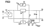
- FIG. 3 shows a basic circuit diagram of such an arrangement.
- 30, 31 designate input terminals to which the AC voltage can be supplied and are connected to a rectifier 32.
- the output of the rectifier is connected to a capacitor 38 and output terminals 39, 40 via a control unit 34.
- the voltage at the output of the rectifier 32 is tapped and fed to a squaring unit 33 and a multiplier 35 via networks (not shown in more detail).
- This signal is fed to a division unit 36, which also receives an error voltage signal V ERR via an operational amplifier 37 operating as a PI controller, which compares and evaluates the output voltage at terminal 39 with a reference voltage U REF .
- This signal is multiplied by the second divided input voltage K iN ⁇ V iN and fed to the controller 34.
- the object of the present invention is a switching power supply to indicate with sinusoidal current consumption, which on the one hand does not have the above-mentioned disadvantage and secondly the Advantages of the quadratic characteristic curve, especially for conventional ones Has supply voltages of 110 or 220 volts.
- the advantage of the arrangement according to the invention is that A so-called division into two linear sub-functions Base part function can be formed, the linear Dependence results in behavior that is more favorable in practice, because at extremely low mains voltages the system Current consumption is limited.
- A represents the quadratic function of a circuit according to the above-mentioned prior art.
- the circuit arrangement according to the invention now replaces this quadratic function in the work area by two linear subfunctions B, C, B being a straight line with the slope m, m> 0 and C being a straight line with the slope 0 and the two straight lines merging at the point U K.
- the errors occurring in the work area can be kept sufficiently low. This applies in particular to the case in which the two intersection points X 1 , X 2 with the quadratic function A are selected for the two main nominal input voltages 110 and 220 volts.
- the linear base area C has proven to be particularly favorable compared to previous solutions, since it results in behavior that is particularly favorable in practice. This measure limits the power consumption from the system at extremely low mains voltages.
- V IN can e.g. B. the RMS value of the rectified input voltage.
- V IN can e.g. B. the RMS value of the rectified input voltage.
- the collector of the pnp transistor 2 is connected to ground and the emitter is connected to a supply voltage source 4 via a current source 3.
- the emitter of transistor 2 is connected to the base of an npn transistor 8. Its emitter is connected to ground via a resistor 9.
- the collector of transistor 8 is connected on the one hand to the base of second pnp transistor 7 and to the collector of a third pnp transistor 5.
- the base of transistor 5 is connected to the base of a fourth pnp transistor 6 and to its collector and the emitter of transistor 7.
- the emitters of the transistors 5 and 6 are connected to one another and to the supply voltage terminal 4.
- the collector of transistor 7 is connected to ground on the one hand via a current source 10 and on the other hand to the emitter of a fifth pnp transistor 12.
- a reference voltage can be fed to the base of the transistor 12 via a terminal 11.
- the collector of transistor 12 is connected to an output terminal 14 and via a current source 13 to the supply voltage terminal.
- the input voltage at 1 is transmitted through the buffer amplifier 2, 3, 8 to the resistance sand 9.
- the current in the collector branch of transistor 8 is approx. I. C8 ⁇ U in R 9
- the current mirror consisting of transistors 5, 6 and 7, the difference between mirror current and the current of the source 10 is formed.
- the transistor 12 couples this current difference as soon as it is positive. To do this the base of transistor 12 via terminal 11 on suitable potential.
- the output current of the Circuit consists of the sum of the collector current of 12 and stream 13.
- the resulting characteristic curve shown in FIG. 2 can be determined as follows:
- the transistor 12 opens only when the values of I k are positive, so that the output current rises from the break voltage U k with the slope 1 / R 9 .
- the constant C is equal to the current I 12 .
Landscapes
- Engineering & Computer Science (AREA)
- Power Engineering (AREA)
- Rectifiers (AREA)
- Control Of Electrical Variables (AREA)
Description
- Figur 1
- eine erfindungsgemäße Schaltungsanordnung zur Bildung der Vorsteuerungsgröße,
- Figur 2
- eine Übertragungsfunktion der erfindungsgemäßen Schaltung gemäß Figur 1 und eine Übertragungsfunktion gemäß dem Stand der Technik.
- Figur 3
- ein Blockschaltbild einer Anordnung gemäß dem Stand der Technik.
Der Strom im Kollektorzweig des Transistors 8 beträgt ca.
Claims (4)
- Schaltnetzteil mit sinusförmiger Stromaufnahmedadurch gekennzeichnet, daßmit einem Gleichrichter (32), dem eine sinusförmige Wechselspannung zuführbar ist und an dessen Ausgang eine gleichgerichtete Wechselspannung abgreifbar ist, wobei die gleichgerichtete Wechselspannung als Eingangssignal (VIN) einer geschalteten Regeleinrichtung (34) zugeführt wird,mit einer Multiplizierereinrichtung (35), der das Eingangssignal der geschalteten Regeleinrichtung (VIN) und ein aus dem Ausgangssignal (39) der geschalteten Regeleinrichtung (34) abgeleitetes Signal zugeführt wird und die die beiden Größen multipliziert und ein Ausgangssignal erzeugt, das der geschalteten Regeleinrichtung (34) zugeführt wird,Schaltmittel (33a) vorgesehen sind, die anhand des Eingangssignals (VIN) ein quasi-quadratisches Signal (D) erzeugen, wobei das quasi-quadratische Signal (D) aus einer mindestens zwei lineare Teilfunktionen (B, C) enthaltenden Übertragungsfunktion gebildet wird, wobei die Übertragungsfunktion das Quadrat des Eingangssignals (VIN) in mindestens zwei Punkten annähert undeine Teilereinrichtung (36) vorgesehen ist, in der das Ausgangssignal der geschalteten Regeleinrichtung (39) durch das quasi-quadratische Eingangssignal (D) geteilt wird, wobei die Teilereinrichtung des abgeleitete Signal erzeugt.
- Schaltnetzteil nach Anspruch 1,
dadurch gekennzeichnet, daß die erste lineare Teilfunktion (C) für die Spannung des Eingangssignals (VIN) von 0 Volt bis zu einer Knickspannung (Uk) mit der Steigung 0 gilt und die zweite lineare Teilfunktion (B) ab der Knickspannung (Uk) eine Gerade mit einer Steigung m hat, wobei m > 0 ist. - Schaltungsanordnung nach Anspruch 1 oder 2,
dadurch gekennzeichnet, daßein Pufferverstärker (2, 3, 8, 9) vorgesehen ist, dem die Eingangsspannung (VIN)zugeführt wird und der eine Last (9) speist,ein Stromspiegel (5, 6, 7) vorgesehen ist, dessen Eingangskreis das Ausgangssignal des ersten Pufferverstärkers (2, 3, 8,9) zugeführt wird und dessen Ausgangsstrom (Ik) der Laststrecke eines Transistors (12) zugeführt wird unddem Steueranschluß des zweiten Transistors (12) eine Referenzspannung (11) zugeführt wird und der Ausgangskreis des zweiten Transistors (12) zum einen mit einer zweiten Stromquelle (13) und zum anderen mit einer Ausgangsklemme (14) verbunden ist. - Schaltungsanordnung nach Anspruch 3,
dadurch gekennzeichnet, daß die Steigung m der zweiten linearen Teilfunktion (B) durch einen Widerstand (9) im Eingangskreis des Stromspiegels (5, 6, 7) einstellbar ist.
Applications Claiming Priority (2)
| Application Number | Priority Date | Filing Date | Title |
|---|---|---|---|
| DE4421806 | 1994-06-22 | ||
| DE4421806A DE4421806C1 (de) | 1994-06-22 | 1994-06-22 | Schaltnetzteil mit sinusförmiger Stromaufnahme |
Publications (2)
| Publication Number | Publication Date |
|---|---|
| EP0689281A1 EP0689281A1 (de) | 1995-12-27 |
| EP0689281B1 true EP0689281B1 (de) | 1998-03-18 |
Family
ID=6521203
Family Applications (1)
| Application Number | Title | Priority Date | Filing Date |
|---|---|---|---|
| EP95109031A Expired - Lifetime EP0689281B1 (de) | 1994-06-22 | 1995-06-12 | Schaltnetzteil mit sinusförmiger Stromaufnahme |
Country Status (3)
| Country | Link |
|---|---|
| US (1) | US5652702A (de) |
| EP (1) | EP0689281B1 (de) |
| DE (2) | DE4421806C1 (de) |
Families Citing this family (1)
| Publication number | Priority date | Publication date | Assignee | Title |
|---|---|---|---|---|
| ATE243384T1 (de) * | 1996-12-18 | 2003-07-15 | Patent Treuhand Ges Fuer Elektrische Gluehlampen Mbh | Elektronisches schaltnetzteil |
Family Cites Families (5)
| Publication number | Priority date | Publication date | Assignee | Title |
|---|---|---|---|---|
| JPS6053924B2 (ja) * | 1978-04-05 | 1985-11-28 | 株式会社東芝 | リミツタ回路 |
| US4677366A (en) * | 1986-05-12 | 1987-06-30 | Pioneer Research, Inc. | Unity power factor power supply |
| US5179528A (en) * | 1989-11-22 | 1993-01-12 | Texas Instruments Incorporated | Signal processing system and method implementing a non-linear transfer function approximated by a piecewise linear transformation |
| DE4105463A1 (de) * | 1991-02-21 | 1992-08-27 | Siemens Ag | Steuerverfahren fuer einen spannungswandler mit grossem eingangsspannungsbereich und die verwendung eines solchen verfahrens |
| IT1248607B (it) * | 1991-05-21 | 1995-01-19 | Cons Ric Microelettronica | Circuito di pilotaggio di un transistore di potenza con una corrente di base funzione predeterminata di quella di collettore |
-
1994
- 1994-06-22 DE DE4421806A patent/DE4421806C1/de not_active Expired - Fee Related
-
1995
- 1995-06-12 DE DE59501623T patent/DE59501623D1/de not_active Expired - Fee Related
- 1995-06-12 EP EP95109031A patent/EP0689281B1/de not_active Expired - Lifetime
- 1995-06-22 US US08/493,808 patent/US5652702A/en not_active Expired - Fee Related
Also Published As
| Publication number | Publication date |
|---|---|
| US5652702A (en) | 1997-07-29 |
| DE59501623D1 (de) | 1998-04-23 |
| DE4421806C1 (de) | 1995-08-10 |
| EP0689281A1 (de) | 1995-12-27 |
Similar Documents
| Publication | Publication Date | Title |
|---|---|---|
| DE2933029C2 (de) | ||
| DE3015162C2 (de) | Anordnung zum Steuern eines Asynchronmotors über einen Frequenzumrichter | |
| EP1103038B1 (de) | Schaltungsanordnung zur messwerterfassung, -übertragung und -auswertung | |
| EP0421516B1 (de) | Stromversorgungseinrichtung mit Spannungsregelung und Strombegrenzung | |
| DE3015610A1 (de) | Schaltung zur regelung eines gleichstroms | |
| DE69824751T2 (de) | Regler | |
| DE2305291B2 (de) | Regelschaltung zur Regelung der Amplitude eines Signals | |
| DE68912408T2 (de) | Stromversorgung, die von veränderlichen Wechselstromeingangsspannungen konstante Gleichstromausgangsspannungen liefert. | |
| DE3727420C2 (de) | Ablenkschaltung | |
| DE3302991A1 (de) | Trigonometrischer funktionsgenerator | |
| EP0698794A1 (de) | Schaltungsanordnung zur Unterspannungs-Erkennung | |
| DE4421806C1 (de) | Schaltnetzteil mit sinusförmiger Stromaufnahme | |
| EP0455062B1 (de) | Stromgespeister Gegentaktwandler | |
| EP0682305B1 (de) | Schaltungsanordnung zur Erzeugung eines Referenzstroms | |
| DE2649306A1 (de) | Spannungsregler fuer generatoren in kraftfahrzeugen | |
| EP0624802B1 (de) | Schaltungsanordnung zum Gleichrichten von Wechselspannungssignalen | |
| EP1205021A1 (de) | Verfahren zur regelung eines schaltnetzteiles und schaltnetzteil | |
| DE2624337A1 (de) | Schaltungsanordnung mit einem gegentaktverstaerker, der zwei emittergekoppelte transistoren enthaelt | |
| DE3012823C2 (de) | ||
| DE2007694C3 (de) | Spannungsregelgerät mit schaltendem Stellglied | |
| CH658520A5 (de) | Schaltungsanordnung zur speisung eines messgroessenumformers. | |
| EP0496023B1 (de) | Verfahren zur Reduzierung der Verlustleistung bei Einrichtungen zur berührungslosen Daten- und Energieübertragung sowie Anordnung zur Durchführung des Verfahrens | |
| DE3527844A1 (de) | Schaltungsanordnung zur frequenzverstellung eines gleichspannungs-zwischenkreisumrichters bei konstanter ausgangsspannung | |
| EP0572491A1 (de) | Steuerverfahren für einen spannungswandler mit grossem eingangsspannungsbereich und die verwendung eines solchen verfahrens. | |
| DE2625288A1 (de) | Anordnung zur regelung einer wechselspannung |
Legal Events
| Date | Code | Title | Description |
|---|---|---|---|
| PUAI | Public reference made under article 153(3) epc to a published international application that has entered the european phase |
Free format text: ORIGINAL CODE: 0009012 |
|
| AK | Designated contracting states |
Kind code of ref document: A1 Designated state(s): DE FR GB IT |
|
| 17P | Request for examination filed |
Effective date: 19960520 |
|
| 17Q | First examination report despatched |
Effective date: 19961209 |
|
| GRAG | Despatch of communication of intention to grant |
Free format text: ORIGINAL CODE: EPIDOS AGRA |
|
| GRAG | Despatch of communication of intention to grant |
Free format text: ORIGINAL CODE: EPIDOS AGRA |
|
| GRAH | Despatch of communication of intention to grant a patent |
Free format text: ORIGINAL CODE: EPIDOS IGRA |
|
| GRAH | Despatch of communication of intention to grant a patent |
Free format text: ORIGINAL CODE: EPIDOS IGRA |
|
| GRAA | (expected) grant |
Free format text: ORIGINAL CODE: 0009210 |
|
| AK | Designated contracting states |
Kind code of ref document: B1 Designated state(s): DE FR GB IT |
|
| REF | Corresponds to: |
Ref document number: 59501623 Country of ref document: DE Date of ref document: 19980423 |
|
| ET | Fr: translation filed | ||
| ITF | It: translation for a ep patent filed | ||
| GBT | Gb: translation of ep patent filed (gb section 77(6)(a)/1977) |
Effective date: 19980520 |
|
| PLBE | No opposition filed within time limit |
Free format text: ORIGINAL CODE: 0009261 |
|
| STAA | Information on the status of an ep patent application or granted ep patent |
Free format text: STATUS: NO OPPOSITION FILED WITHIN TIME LIMIT |
|
| 26N | No opposition filed | ||
| PGFP | Annual fee paid to national office [announced via postgrant information from national office to epo] |
Ref country code: GB Payment date: 19990616 Year of fee payment: 5 |
|
| PGFP | Annual fee paid to national office [announced via postgrant information from national office to epo] |
Ref country code: FR Payment date: 19990629 Year of fee payment: 5 |
|
| PGFP | Annual fee paid to national office [announced via postgrant information from national office to epo] |
Ref country code: DE Payment date: 19990820 Year of fee payment: 5 |
|
| PG25 | Lapsed in a contracting state [announced via postgrant information from national office to epo] |
Ref country code: GB Free format text: LAPSE BECAUSE OF NON-PAYMENT OF DUE FEES Effective date: 20000612 |
|
| GBPC | Gb: european patent ceased through non-payment of renewal fee |
Effective date: 20000612 |
|
| PG25 | Lapsed in a contracting state [announced via postgrant information from national office to epo] |
Ref country code: FR Free format text: LAPSE BECAUSE OF NON-PAYMENT OF DUE FEES Effective date: 20010228 |
|
| REG | Reference to a national code |
Ref country code: FR Ref legal event code: ST |
|
| PG25 | Lapsed in a contracting state [announced via postgrant information from national office to epo] |
Ref country code: DE Free format text: LAPSE BECAUSE OF NON-PAYMENT OF DUE FEES Effective date: 20010403 |
|
| PG25 | Lapsed in a contracting state [announced via postgrant information from national office to epo] |
Ref country code: IT Free format text: LAPSE BECAUSE OF NON-PAYMENT OF DUE FEES;WARNING: LAPSES OF ITALIAN PATENTS WITH EFFECTIVE DATE BEFORE 2007 MAY HAVE OCCURRED AT ANY TIME BEFORE 2007. THE CORRECT EFFECTIVE DATE MAY BE DIFFERENT FROM THE ONE RECORDED. Effective date: 20050612 |