EP0689290A1 - Semiconductor integrated circuit having reset circuit - Google Patents
Semiconductor integrated circuit having reset circuit Download PDFInfo
- Publication number
- EP0689290A1 EP0689290A1 EP95109742A EP95109742A EP0689290A1 EP 0689290 A1 EP0689290 A1 EP 0689290A1 EP 95109742 A EP95109742 A EP 95109742A EP 95109742 A EP95109742 A EP 95109742A EP 0689290 A1 EP0689290 A1 EP 0689290A1
- Authority
- EP
- European Patent Office
- Prior art keywords
- circuit
- semiconductor integrated
- reset
- integrated circuit
- reset signal
- Prior art date
- Legal status (The legal status is an assumption and is not a legal conclusion. Google has not performed a legal analysis and makes no representation as to the accuracy of the status listed.)
- Withdrawn
Links
- 239000004065 semiconductor Substances 0.000 title claims abstract description 73
- 230000003111 delayed effect Effects 0.000 claims description 11
- 230000003247 decreasing effect Effects 0.000 abstract description 5
- 230000004044 response Effects 0.000 description 11
- 238000010586 diagram Methods 0.000 description 7
- 230000008859 change Effects 0.000 description 5
- 239000003990 capacitor Substances 0.000 description 1
- 230000007547 defect Effects 0.000 description 1
- 230000007257 malfunction Effects 0.000 description 1
- 230000004048 modification Effects 0.000 description 1
- 238000012986 modification Methods 0.000 description 1
- 230000007704 transition Effects 0.000 description 1
Images

Classifications
-
- H—ELECTRICITY
- H03—ELECTRONIC CIRCUITRY
- H03K—PULSE TECHNIQUE
- H03K5/00—Manipulating of pulses not covered by one of the other main groups of this subclass
- H03K5/15—Arrangements in which pulses are delivered at different times at several outputs, i.e. pulse distributors
- H03K5/15013—Arrangements in which pulses are delivered at different times at several outputs, i.e. pulse distributors with more than two outputs
- H03K5/1506—Arrangements in which pulses are delivered at different times at several outputs, i.e. pulse distributors with more than two outputs with parallel driven output stages; with synchronously driven series connected output stages
-
- H—ELECTRICITY
- H03—ELECTRONIC CIRCUITRY
- H03K—PULSE TECHNIQUE
- H03K17/00—Electronic switching or gating, i.e. not by contact-making and –breaking
- H03K17/22—Modifications for ensuring a predetermined initial state when the supply voltage has been applied
Definitions
- the present invention relates to a semiconductor integrated circuit, and more specifically to a semiconductor integrated circuit having a reset circuit.
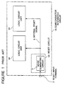
- a semiconductor integrated circuit having a reset circuit is so configured as shown in Figure 1 that a reset signal applied through a reset input terminal 2 of a semiconductor integrated circuit 1A is caused to pass through a noise eliminating circuit 5 and then applied to all various internal logic circuit units within the semiconductor integrated circuit 1A at the same timing.
- the semiconductor integrated circuit 1A actually includes a number of logic circuit units, but only two logic circuit units 3A and 3B are shown in Figure 1 for simplification of the drawing.
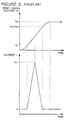
- i1 represents an increased amount of the consumed current of the semiconductor integrated circuit 1A when all the internal logic circuit units 3A and 3B are simultaneously reset by the internal reset signal 6.
- the increased current amount i1 is a sum of pass-through currents which flows from a power supply to ground through various transistors activated in response to the internal reset signal 6.
- i0 represents a consumed current of the semiconductor integrated circuit 1A when the reset signal is not applied.
- a pass-through current of a CMOS inverter is discussed assuming that respective thresholds of an nMOS transistor and a pMOS transistor constituting the CMOS inverter are Vtn and Vtp, and a power supply voltage is V DD .
- a peak value of the pass-through current reaches for example 0.5 mA.
- the semiconductor integrated circuit 1A operates with the power supply voltage of 5 V and the consumed electric power of 0.1 W
- the current i0 is 20 mA. Accordingly, assuming that the reset signal is applied simultaneously to the CMOS inverters (not shown) in the logic circuit units 3A and 3B, the increased current amount i1 reaches 30 mA to 50 mA in the case of 100 CMOS inverters and 300 mA to 500 mA in the case of 1000 CMOS inverters.
- Another object of the present invention is to provide a semiconductor integrated circuit having a reset circuit, configured to minimize noises appearing on the power supply voltage and the ground voltage and also to prevent generation of the latch-up phenomenon.
- a semiconductor integrated circuit having a plurality of logic circuit units and a reset circuit, wherein the reset circuit generates at different timings a plurality of internal reset signals, which are supplied to the plurality of logic circuit units, respectively.
- the reset circuit includes an input circuit receiving an external reset signal to generate a first internal reset signal, and (N-1) delay circuits (where N is a positive integer larger than 1) receiving the first internal reset signal and each generating a delayed internal reset signal, so that, N internal reset signals in total are generated at different timings.
- the semiconductor integrated circuit excluding the reset circuit is divided into N logic circuit units (where N is an positive integer larger than 1) which have substantially the same current amount increased when the logic circuit units are reset by the internal reset signals, and if N internal reset signals are generated at different timings, the increased current peak at the time of a resetting can be decreased to l/N of the increased current peak when all the N logic circuit units are reset at the same timing.
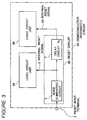
- FIG. 3 there is shown a block diagram of a first embodiment of the semiconductor integrated circuit having a reset circuit in accordance with the present invention.
- the shown semiconductor integrated circuit is generally designated by Reference Numeral 1B, and has an external reset input terminal 2 for receiving an external reset signal and a reset circuit 4B having an input connected to the external reset input terminal 2.
- the semiconductor integrated circuit 1B excluding the reset circuit 4B is divided into two logic circuit units 3A and 3B.
- the reset circuit 4B includes a noise eliminating circuit 5 receiving the external reset signal supplied through the external reset input terminal 2 for generating a first internal reset signal 6, which is supplied to the logic circuit unit 3A.
- the reset circuit 4B also includes a delay circuit 7 of a delay time T0 receiving the first internal reset signal 6 for outputting a second and delayed internal reset signal 6A, which is supplied to the logic circuit unit 3B.
- the semiconductor integrated circuit 1B excluding the reset circuit 4B is divided into the logic circuit units 3A and 3B so as to ensure the relation that the ratio of the increased amount of the consumed current in the logic circuit unit 3A in response to the internal reset signal 6 to the increased amount of the consumed current in the logic circuit unit 3B in response to the internal reset signal 6A, is K:L (where K and L are positive integer).
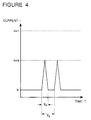
- the first internal reset signal 6 is activated for a first place, so that the logic circuit unit 3A is reset, with the result that the consumed current of the semiconductor integrated circuit 1B increases by i2, as shown in Figure 4.
- Ts represents a time period in which a pass-through current flows.
- the second internal reset signal 6A is activated, so that the logic circuit unit 3B is reset.
- the delay time of the delay circuit 7 is T0 and the time period in which the pass-through current flows is Ts under the assumption that a waveform of the pass-through current is substantially an isosceles triangle
- the case shown in Figure 4 corresponds to a situation of T0>Ts
- T0 ⁇ (1/2)Ts the pass-through current in the logic circuit unit 3A considerably overlaps the pass-through current in the logic circuit unit 3B in time, so that the maximum current exceeds i0+i2. Therefore, it is preferred to set T0 ⁇ (1/2)Ts . As a matter of course, however, it cannot be said that the larger the delay time T0 is, it is more preferable.
- the delay time T0 is to be set within such a range that the semiconductor integrated circuit never malfunctions.
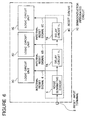
- FIG. 6 there is shown a block diagram of a second embodiment of the semiconductor integrated circuit having a reset circuit in accordance with the present invention.
- the second semiconductor integrated circuit is generally designated by Reference Numeral 1C, and has an external reset input terminal 2 for receiving an external reset signal and a reset circuit 4C having an input connected to the external reset input terminal 2.
- the semiconductor integrated circuit 1C excluding the reset circuit 4C is divided into three logic circuit units 3C, 3D and 3E.
- the reset circuit 4C includes a noise eliminating circuit 5 receiving the external reset signal supplied through the external reset input terminal 2 for generating a first internal reset signal 6, which is supplied to the logic circuit unit 3C.
- the reset circuit 4C also includes a delay circuit 7A of a delay time T1 receiving the first internal reset signal 6 for outputting a second and delayed internal reset signal 6B, which is supplied to the logic circuit unit 3D.
- the reset circuit 4C includes a delay circuit 7B of a delay time T2 receiving the second and delayed internal reset signal 6B for outputting a third and delayed internal reset signal 6C, which is supplied to the logic circuit unit 3D.
- the semiconductor integrated circuit 1C excluding the reset circuit 4C is divided into the logic circuit units 3C, 3D and 3E so as to ensure the relation that the increased amount of the consumed current in the logic circuit unit 3C in response to the internal reset signal 6, the increased amount of the consumed current in the logic circuit unit 3D in response to the internal reset signal 6B, and the increased amount of the consumed current in the logic circuit unit 3E in response to the internal reset signal 6C, are in proportion of K:L:M (where K, L and M are positive integer).
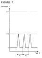
- the first internal reset signal 6 is activated for a first place, so that the logic circuit unit 3C is reset, with the result that the consumed current of the semiconductor integrated circuit 1C increases by i3, as shown in Figure 7.
- the second internal reset signal 6B is activated, so that the logic circuit unit 3D is reset. Therefore, the consumed current of the semiconductor integrated circuit 1C increases by i3, again, after a delay of T1 from the increase of the consumed current of the semiconductor integrated circuit 1C caused by resetting the logic circuit unit 3C.
- the third internal reset signal 6C is activated, so that the logic circuit unit 3E is reset. Therefore, the consumed current of the semiconductor integrated circuit 1C increases by i3, again, after a delay of T2 from the increase of the consumed current of the semiconductor integrated circuit 1C caused by resetting the logic circuit unit 3D.
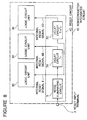
- FIG 8 there is shown a block diagram of a third embodiment of the semiconductor integrated circuit having a reset circuit in accordance with the present invention.
- elements similar to those shown in Figure 6 are given the same Reference Numerals, and explanation thereof will be omitted for simplification of the description.
- the third embodiment is different from the second embodiment in that the third embodiment includes, in place of the delay circuit 7B, a delay circuit 7C having a delay time of T1+T2 and receiving the first internal reset signal 6 for outputting a third and delayed internal reset signal 6D to the logic circuit unit 3E.
- the delay circuit 7C is connected in parallel to the delay circuit 7A.
- the third embodiment operates similarly to the second embodiment, and therefore, explanation of operation of the third embodiment will be omitted.
- (N-1) delay circuits are cascaded after the noise eliminating circuit 5 in such a manner that a first one of the delay circuits receives the first internal reset signal and a second one of the delay circuits receives an output of the first one, and so on, or if (N-1) delay circuits having different delay times are connected in parallel to each other to receive the internal reset signal outputted from the noise eliminating circuit 5, so that N internal reset signals in total are generated at different timings from the noise eliminating circuit 5 and the (N-1) delay circuits within the semiconductor integrated circuit, and if the semiconductor integrated circuit excluding the reset circuit is divided into N logic circuit units receiving the N different internal reset signals, respectively, the N logic circuit units are reset at the N different timings, and therefore, the increased amount of the consumed current caused by the resetting can be reduced.
- the semiconductor integrated circuit excluding the reset circuit is divided in such a manner that the N logic circuit units have substantially the same increased amount of the consumed current caused by the resetting, the increased amount of the consumed current caused by the resetting can be reduced to l/N in comparison with the case in which all the circuits within the semiconductor integrated circuit are reset simultaneously.
- the delay circuits 7 and 7A to 7C can be formed of an inverter or cascaded inverters or a combination of an inverter and a capacitor, as well known to persons skilled in the art.
Landscapes
- Physics & Mathematics (AREA)
- Nonlinear Science (AREA)
- Electronic Switches (AREA)
- Static Random-Access Memory (AREA)
- Semiconductor Integrated Circuits (AREA)
- Dram (AREA)
- Logic Circuits (AREA)
Abstract
In a semiconductor integrated circuit (1B,1C) having a reset circuit (4B,4C), the semiconductor integrated circuit (1B,1C) excluding the reset circuit (4B,4C) is divided into a plurality of logic circuit units (3A...3E), and the reset circuit (4B,4C) is configured to generate at different timings a plurality of internal reset signals (6,6A...6D), which are supplied to the plurality of logic circuit units (3A...3E), respectively. With this arrangement, the increased current peak at the time of a resetting can be decreased, so that the noises appearing on the power supply voltage and the ground voltage can be suppressed and a latch-up phenomenon can be prevented.
Description
- The present invention relates to a semiconductor integrated circuit, and more specifically to a semiconductor integrated circuit having a reset circuit.
- In the prior art, a semiconductor integrated circuit having a reset circuit is so configured as shown in Figure 1 that a reset signal applied through a
reset input terminal 2 of a semiconductor integratedcircuit 1A is caused to pass through anoise eliminating circuit 5 and then applied to all various internal logic circuit units within the semiconductor integratedcircuit 1A at the same timing. Here, the semiconductor integratedcircuit 1A actually includes a number of logic circuit units, but only twologic circuit units - In the circuit shown in Figure 1, if the reset signal is applied to the
reset input terminal 2, aninternal reset signal 6 is generated from aninternal reset circuit 4A, and the internallogic circuit units internal reset signal 6. In other words, all the internal logic circuit units internally included in the semiconductor integratedcircuit 1A excluding thereset circuit 4A are reset simultaneously. As a result, When the reset signal is applied, a consumed current of the semiconductor integratedcircuit 1A increases by i₁ as shown in Figure 2. - In Figure 2, i₁ represents an increased amount of the consumed current of the semiconductor integrated
circuit 1A when all the internallogic circuit units internal reset signal 6. In other words, the increased current amount i₁ is a sum of pass-through currents which flows from a power supply to ground through various transistors activated in response to theinternal reset signal 6. On the other hand, i₀ represents a consumed current of the semiconductor integratedcircuit 1A when the reset signal is not applied. - Here, a pass-through current of a CMOS inverter is discussed assuming that respective thresholds of an nMOS transistor and a pMOS transistor constituting the CMOS inverter are Vtn and Vtp, and a power supply voltage is VDD. As shown in Figure 2, when an input signal Vin applied to the CMOS inverter ("RESET SIGNAL VOLTAGE" in Figure 2) rises up or falls down, during a transition period fulfilling the condition :

- Therefore, if the semiconductor integrated
circuit 1A operates with the power supply voltage of 5 V and the consumed electric power of 0.1 W, the current i₀ is 20 mA. Accordingly, assuming that the reset signal is applied simultaneously to the CMOS inverters (not shown) in thelogic circuit units - If such a large pass-through current flows from the power supply to the ground, namely, if a large current flows through the semiconductor integrated
circuit 1A, noises appears on the power supply and the ground so that the power supply voltage and the ground voltage varies, and a latch-up resistance drops. - Accordingly, it is an object of the present invention to provide a semiconductor integrated circuit having a reset circuit, which has overcome the above mentioned defect of the conventional one.
- Another object of the present invention is to provide a semiconductor integrated circuit having a reset circuit, configured to minimize noises appearing on the power supply voltage and the ground voltage and also to prevent generation of the latch-up phenomenon.
- The above and other objects of the present invention are achieved in accordance with the present invention by a semiconductor integrated circuit having a plurality of logic circuit units and a reset circuit, wherein the reset circuit generates at different timings a plurality of internal reset signals, which are supplied to the plurality of logic circuit units, respectively.
- Preferably, the reset circuit includes an input circuit receiving an external reset signal to generate a first internal reset signal, and (N-1) delay circuits (where N is a positive integer larger than 1) receiving the first internal reset signal and each generating a delayed internal reset signal, so that, N internal reset signals in total are generated at different timings.
- With the above mentioned arrangement, a plurality of internal reset signals generated at different timings, are supplied to a plurality of logic circuit units, respectively. Therefore, the increased current peak at the time of a resetting can be decreased, so that the noises appearing on the power supply voltage and the ground voltage can be suppressed and a latch-up phenomenon can be prevented.
- Therefore, if the semiconductor integrated circuit excluding the reset circuit is divided into N logic circuit units (where N is an positive integer larger than 1) which have substantially the same current amount increased when the logic circuit units are reset by the internal reset signals, and if N internal reset signals are generated at different timings, the increased current peak at the time of a resetting can be decreased to l/N of the increased current peak when all the N logic circuit units are reset at the same timing.
- The above and other objects, features and advantages of the present invention will be apparent from the following description of preferred embodiments of the invention with reference to the accompanying drawings.
-
- Figure 1 is a block diagram of a conventional semiconductor integrated circuit having a reset circuit;
- Figure 2 is a pair of graphs showing a voltage change of the reset signal and a current change in the conventional semiconductor integrated circuit shown in Figure 1 when the reset signal is applied;
- Figure 3 is a block diagram of a first embodiment of the semiconductor integrated circuit having a reset circuit in accordance with the present invention;
- Figure 4 is a graph showing a current change in the semiconductor integrated circuit shown in Figure 3 when the reset signal is applied;
- Figures 5A and 5B are graphs showing a relation between the delay time and the current change in the semiconductor integrated circuit shown in Figure 3;
- Figure 6 is a block diagram of a second embodiment of the semiconductor integrated circuit having a reset circuit in accordance with the present invention;
- Figure 7 is a graph showing a current change in the semiconductor integrated circuit shown in Figure 6 when the reset signal is applied; and
- Figure 8 is a block diagram of a third embodiment of the semiconductor integrated circuit having a reset circuit in accordance with the present invention.
- Referring to Figure 3, there is shown a block diagram of a first embodiment of the semiconductor integrated circuit having a reset circuit in accordance with the present invention.
- The shown semiconductor integrated circuit is generally designated by
Reference Numeral 1B, and has an externalreset input terminal 2 for receiving an external reset signal and areset circuit 4B having an input connected to the externalreset input terminal 2. The semiconductor integratedcircuit 1B excluding thereset circuit 4B is divided into twologic circuit units reset circuit 4B includes anoise eliminating circuit 5 receiving the external reset signal supplied through the externalreset input terminal 2 for generating a firstinternal reset signal 6, which is supplied to thelogic circuit unit 3A. Thereset circuit 4B also includes adelay circuit 7 of a delay time T₀ receiving the firstinternal reset signal 6 for outputting a second and delayedinternal reset signal 6A, which is supplied to thelogic circuit unit 3B. - In this embodiment, the semiconductor integrated
circuit 1B excluding thereset circuit 4B is divided into thelogic circuit units logic circuit unit 3A in response to theinternal reset signal 6 to the increased amount of the consumed current in thelogic circuit unit 3B in response to theinternal reset signal 6A, is K:L (where K and L are positive integer). - Now, assuming that

logic circuit unit 3A in response to theinternal reset signal 6 is equal to the increased amount of the consumed current in thelogic circuit unit 3B in response to theinternal reset signal 6A, operation of the first embodiment will be described. - When the external reset signal is applied to the
reset input terminal 2, the firstinternal reset signal 6 is activated for a first place, so that thelogic circuit unit 3A is reset, with the result that the consumed current of the semiconductor integratedcircuit 1B increases by i₂, as shown in Figure 4. - Here, i₂ is the increased amount of the consumed current in the
logic circuit unit 3A when thelogic circuit unit 3A is reset, and therefore, it can be expressed :
integrated circuit 1B when thelogic circuit units reset signal 6. In Figure 4, Ts represents a time period in which a pass-through current flows. - After the delay time T₀ from the moment the first
internal reset signal 6 was activated, the secondinternal reset signal 6A is activated, so that thelogic circuit unit 3B is reset. As mentioned above, since the increased amount of the consumed current in thelogic circuit unit 3A in response to theinternal reset signal 6 is equal to the increased amount of the consumed current in thelogic circuit unit 3B in response to theinternal reset signal 6A
integrated circuit 1B increases by i₂, again, after a delay of T₀ from the increase of the consumed current of the semiconductor integratedcircuit 1B caused by resetting thelogic circuit unit 3A. - Thus, by dividing the semiconductor integrated
circuit 1B into the twologic circuit units internal reset signals circuit 1B so as to supply the twointernal reset signals logic circuit units logic circuit units 
- Here, assuming that the delay time of the
delay circuit 7 is T₀ and the time period in which the pass-through current flows is Ts under the assumption that a waveform of the pass-through current is substantially an isosceles triangle, the case shown in Figure 4 corresponds to a situation of T₀>Ts, and the maximum current of the semiconductor integrated circuit is i₀+i₂ (where


- As shown in Figure 5B, however, if

logic circuit unit 3A considerably overlaps the pass-through current in thelogic circuit unit 3B in time, so that the maximum current exceeds i₀+i₂. Therefore, it is preferred to set
- Assuming that "I" represents the increased amount of the consumed current in the semiconductor integrated circuit when the both of the
logic circuit units 
- Referring to Figure 6, there is shown a block diagram of a second embodiment of the semiconductor integrated circuit having a reset circuit in accordance with the present invention.
- The second semiconductor integrated circuit is generally designated by
Reference Numeral 1C, and has an externalreset input terminal 2 for receiving an external reset signal and areset circuit 4C having an input connected to the externalreset input terminal 2. The semiconductor integratedcircuit 1C excluding thereset circuit 4C is divided into threelogic circuit units reset circuit 4C includes anoise eliminating circuit 5 receiving the external reset signal supplied through the externalreset input terminal 2 for generating a firstinternal reset signal 6, which is supplied to thelogic circuit unit 3C. Thereset circuit 4C also includes adelay circuit 7A of a delay time T₁ receiving the firstinternal reset signal 6 for outputting a second and delayedinternal reset signal 6B, which is supplied to thelogic circuit unit 3D. Furthermore, thereset circuit 4C includes adelay circuit 7B of a delay time T₂ receiving the second and delayedinternal reset signal 6B for outputting a third and delayed internal reset signal 6C, which is supplied to thelogic circuit unit 3D. - In this second embodiment, the semiconductor integrated
circuit 1C excluding thereset circuit 4C is divided into thelogic circuit units logic circuit unit 3C in response to theinternal reset signal 6, the increased amount of the consumed current in thelogic circuit unit 3D in response to theinternal reset signal 6B, and the increased amount of the consumed current in thelogic circuit unit 3E in response to the internal reset signal 6C, are in proportion of K:L:M (where K, L and M are positive integer). - As the most typical example, assuming that

- When the external reset signal is applied to the
reset input terminal 2, the firstinternal reset signal 6 is activated for a first place, so that thelogic circuit unit 3C is reset, with the result that the consumed current of the semiconductor integratedcircuit 1C increases by i₃, as shown in Figure 7. - Here, i₃ is the increased amount of the consumed current in the
logic circuit unit 3C when thelogic circuit unit 3C is reset, and therefore, it can be expressed :
circuit 1C when the threelogic circuit units reset signal 6. - After the delay time T₁ from the moment the first
internal reset signal 6 was activated, the secondinternal reset signal 6B is activated, so that thelogic circuit unit 3D is reset. Therefore, the consumed current of the semiconductor integratedcircuit 1C increases by i₃, again, after a delay of T₁ from the increase of the consumed current of the semiconductor integratedcircuit 1C caused by resetting thelogic circuit unit 3C. - Furthermore, after the delay time T₂ from the moment the second
internal reset signal 6B was activated, the third internal reset signal 6C is activated, so that thelogic circuit unit 3E is reset. Therefore, the consumed current of the semiconductor integratedcircuit 1C increases by i₃, again, after a delay of T₂ from the increase of the consumed current of the semiconductor integratedcircuit 1C caused by resetting thelogic circuit unit 3D. - Thus, by dividing the semiconductor integrated
circuit 1C into the threelogic circuit units circuit 1C so as to supply the three internal reset signals 6, 6B and 6C to the threelogic circuit units logic circuit units 
- Assuming that "I" represents the increased amount of the consumed current in the semiconductor integrated circuit when all of the
logic circuit units 
- Referring to Figure 8, there is shown a block diagram of a third embodiment of the semiconductor integrated circuit having a reset circuit in accordance with the present invention. In Figure 8, elements similar to those shown in Figure 6 are given the same Reference Numerals, and explanation thereof will be omitted for simplification of the description.
- As seen from comparison between Figures 6 and 8, the third embodiment is different from the second embodiment in that the third embodiment includes, in place of the
delay circuit 7B, adelay circuit 7C having a delay time of T₁+T₂ and receiving the firstinternal reset signal 6 for outputting a third and delayed internal reset signal 6D to thelogic circuit unit 3E. Namely, thedelay circuit 7C is connected in parallel to thedelay circuit 7A. - Therefore, since the internal reset signal 6D is substantially the same as the internal reset signal 6C, the third embodiment operates similarly to the second embodiment, and therefore, explanation of operation of the third embodiment will be omitted.
- Accordingly, generally speaking, if (N-1) delay circuits are cascaded after the
noise eliminating circuit 5 in such a manner that a first one of the delay circuits receives the first internal reset signal and a second one of the delay circuits receives an output of the first one, and so on, or if (N-1) delay circuits having different delay times are connected in parallel to each other to receive the internal reset signal outputted from thenoise eliminating circuit 5, so that N internal reset signals in total are generated at different timings from thenoise eliminating circuit 5 and the (N-1) delay circuits within the semiconductor integrated circuit, and if the semiconductor integrated circuit excluding the reset circuit is divided into N logic circuit units receiving the N different internal reset signals, respectively, the N logic circuit units are reset at the N different timings, and therefore, the increased amount of the consumed current caused by the resetting can be reduced. - In this case, if the semiconductor integrated circuit excluding the reset circuit is divided in such a manner that the N logic circuit units have substantially the same increased amount of the consumed current caused by the resetting, the increased amount of the consumed current caused by the resetting can be reduced to l/N in comparison with the case in which all the circuits within the semiconductor integrated circuit are reset simultaneously.
- Incidentally, the
delay circuits - The invention has thus been shown and described with reference to the specific embodiments. However, it should be noted that the present invention is in no way limited to the details of the illustrated structures but changes and modifications may be made.
Claims (9)
- A semiconductor integrated circuit having a plurality of logic circuit units and a reset circuit, wherein said reset circuit generates at different timings a plurality of internal reset signals, which are supplied to said plurality of logic circuit units, respectively.
- A semiconductor integrated circuit claimed in Claim 1 wherein said reset circuit includes an input circuit receiving an external reset signal to generate a first internal reset signal, and (N-1) delay circuits (where N is a positive integer larger than 1) receiving said first internal reset signal and each generating a delayed internal reset signal, so that, N internal reset signals in total are generated at different timings.
- A semiconductor integrated circuit claimed in Claim 2 wherein said (N-1) delay circuits are cascaded.
- A semiconductor integrated circuit claimed in Claim 2 wherein said (N-1) delay circuits are connected in parallel to each other so that each of said (N-1) delay circuits receives said output of said input circuit, and said (N-1) delay circuits have different delay times, so that said N delayed internal reset signals are generated at different timings from said internal circuit and said (N-1) delay circuits, respectively.
- A semiconductor integrated circuit claimed in Claim 2 wherein said plurality of logic circuit units have substantially the same current amount increased when said logic circuit units receive the internal reset signals.
- A semiconductor integrated circuit having at least an external reset input terminal and a reset circuit receiving an external reset signal through said external reset input terminal, the semiconductor integrated circuit excluding said reset circuit being divided into a plurality of logic circuits units, and said reset circuit including an input circuit receiving said external reset signal to generate a first internal reset signal, and a plurality of delay circuits receiving said first internal reset signal and each generating a delayed internal reset signal at a different timing, said first internal reset signal outputted from said input circuit and said delayed internal reset signals outputted from said delay circuits, respectively, being supplied to said plurality of logic circuits units, respectively, so that said plurality of logic circuits units are reset at different timings.
- A semiconductor integrated circuit claimed in Claim 6 wherein said delay circuits are cascaded in such a manner that a first one of said delay circuits receives said first internal reset signal and a second one of said delay circuits receives an output of said first one, and so on.
- A semiconductor integrated circuit claimed in Claim 6 wherein said delay circuits are connected in parallel to each other so that each of said delay circuits receives said first internal reset signal, and said delay circuits have different delay times, so that delayed internal reset signals are generated at different timings from said delay circuits.
- A semiconductor integrated circuit claimed in Claim 6 wherein said plurality of logic circuit units have substantially the same current amount increased when said logic circuit units receive the internal reset signals.
Applications Claiming Priority (2)
| Application Number | Priority Date | Filing Date | Title |
|---|---|---|---|
| JP162900/94 | 1994-06-22 | ||
| JP6162900A JP2682453B2 (en) | 1994-06-22 | 1994-06-22 | Semiconductor integrated circuit |
Publications (1)
| Publication Number | Publication Date |
|---|---|
| EP0689290A1 true EP0689290A1 (en) | 1995-12-27 |
Family
ID=15763377
Family Applications (1)
| Application Number | Title | Priority Date | Filing Date |
|---|---|---|---|
| EP95109742A Withdrawn EP0689290A1 (en) | 1994-06-22 | 1995-06-22 | Semiconductor integrated circuit having reset circuit |
Country Status (3)
| Country | Link |
|---|---|
| EP (1) | EP0689290A1 (en) |
| JP (1) | JP2682453B2 (en) |
| KR (1) | KR960002803A (en) |
Cited By (3)
| Publication number | Priority date | Publication date | Assignee | Title |
|---|---|---|---|---|
| US6631467B1 (en) * | 2000-02-18 | 2003-10-07 | Mitsubishi Denki Kabushiki Kaisha | Microcomputer timing control circuit provided with internal reset signal generator triggered by external reset signal |
| US7519926B2 (en) | 2005-03-28 | 2009-04-14 | Fujitsu Microelectronics Limited | Semiconductor device and method for designing the same |
| CN112185437A (en) * | 2019-07-03 | 2021-01-05 | 美光科技公司 | Memory with configurable die power-on delay |
Citations (2)
| Publication number | Priority date | Publication date | Assignee | Title |
|---|---|---|---|---|
| US3622809A (en) * | 1969-03-12 | 1971-11-23 | Chemical Bank | Active delay line |
| US4420696A (en) * | 1980-02-25 | 1983-12-13 | Hitachi, Ltd. | Pulse train producing apparatus |
Family Cites Families (4)
| Publication number | Priority date | Publication date | Assignee | Title |
|---|---|---|---|---|
| JPS6055916B2 (en) * | 1980-09-26 | 1985-12-07 | 日本電気株式会社 | timing circuit |
| JPS5914195A (en) * | 1982-07-13 | 1984-01-25 | Nec Corp | Semiconductor device |
| JPS61191280A (en) * | 1985-02-18 | 1986-08-25 | Toshiba Corp | Drive control circuit of brush motor |
| JPH0437309A (en) * | 1990-06-01 | 1992-02-07 | Nec Ic Microcomput Syst Ltd | Electric circuit with power-on reset circuit |
-
1994
- 1994-06-22 JP JP6162900A patent/JP2682453B2/en not_active Expired - Fee Related
-
1995
- 1995-06-22 KR KR1019950016811A patent/KR960002803A/en not_active Ceased
- 1995-06-22 EP EP95109742A patent/EP0689290A1/en not_active Withdrawn
Patent Citations (2)
| Publication number | Priority date | Publication date | Assignee | Title |
|---|---|---|---|---|
| US3622809A (en) * | 1969-03-12 | 1971-11-23 | Chemical Bank | Active delay line |
| US4420696A (en) * | 1980-02-25 | 1983-12-13 | Hitachi, Ltd. | Pulse train producing apparatus |
Non-Patent Citations (2)
| Title |
|---|
| DATABASE WPI Derwent World Patents Index; * |
| PATENT ABSTRACTS OF JAPAN * |
Cited By (4)
| Publication number | Priority date | Publication date | Assignee | Title |
|---|---|---|---|---|
| US6631467B1 (en) * | 2000-02-18 | 2003-10-07 | Mitsubishi Denki Kabushiki Kaisha | Microcomputer timing control circuit provided with internal reset signal generator triggered by external reset signal |
| US7519926B2 (en) | 2005-03-28 | 2009-04-14 | Fujitsu Microelectronics Limited | Semiconductor device and method for designing the same |
| CN112185437A (en) * | 2019-07-03 | 2021-01-05 | 美光科技公司 | Memory with configurable die power-on delay |
| CN112185437B (en) * | 2019-07-03 | 2024-05-31 | 美光科技公司 | Memory with configurable die power-up delay |
Also Published As
| Publication number | Publication date |
|---|---|
| JPH088706A (en) | 1996-01-12 |
| KR960002803A (en) | 1996-01-26 |
| JP2682453B2 (en) | 1997-11-26 |
Similar Documents
| Publication | Publication Date | Title |
|---|---|---|
| US6914462B2 (en) | Power-on reset circuit and method | |
| KR100231091B1 (en) | Level shifter circuit | |
| EP0150480A2 (en) | Power-on reset pulse generator | |
| US20010000425A1 (en) | Level shift circuit | |
| US4902907A (en) | Reset signal generating circuit | |
| US5315187A (en) | Self-controlled output stage with low power bouncing | |
| EP0606912A2 (en) | Polyphase clock generation circuit | |
| CN100517502C (en) | Power up circuit in semiconductor memory device | |
| US6121813A (en) | Delay circuit having a noise reducing function | |
| JP3005169B2 (en) | Reset circuit | |
| US20050110522A1 (en) | Multistage dynamic domino circuit with internally generated delay reset clock | |
| US6016070A (en) | Pulse extending circuit | |
| US4625126A (en) | Clock generator for providing non-overlapping clock signals | |
| US6414517B1 (en) | Input buffer circuits with input signal boost capability and methods of operation thereof | |
| US4472645A (en) | Clock circuit for generating non-overlapping pulses | |
| US6134252A (en) | Enhanced glitch removal circuit | |
| EP0689290A1 (en) | Semiconductor integrated circuit having reset circuit | |
| JP2988387B2 (en) | Semiconductor device | |
| US20010017563A1 (en) | Pulse generator | |
| JP5319230B2 (en) | Semiconductor integrated circuit | |
| US4896056A (en) | Semiconductor IC including circuit for preventing erroneous operation caused by power source noise | |
| EP0342735B1 (en) | Circuit for generating a pulse-shaped signal | |
| EP0459457A2 (en) | Output driver | |
| US6150844A (en) | High voltage tolerance output stage | |
| US5319262A (en) | Low power TTL/CMOS receiver circuit |
Legal Events
| Date | Code | Title | Description |
|---|---|---|---|
| PUAI | Public reference made under article 153(3) epc to a published international application that has entered the european phase |
Free format text: ORIGINAL CODE: 0009012 |
|
| AK | Designated contracting states |
Kind code of ref document: A1 Designated state(s): DE FR GB |
|
| 17P | Request for examination filed |
Effective date: 19960328 |
|
| 17Q | First examination report despatched |
Effective date: 19970220 |
|
| STAA | Information on the status of an ep patent application or granted ep patent |
Free format text: STATUS: THE APPLICATION IS DEEMED TO BE WITHDRAWN |
|
| 18D | Application deemed to be withdrawn |
Effective date: 19970903 |