EP0690391A1 - Circuit intégré d'application spécifique comprenant des fonctions programmables - Google Patents
Circuit intégré d'application spécifique comprenant des fonctions programmables Download PDFInfo
- Publication number
- EP0690391A1 EP0690391A1 EP95850126A EP95850126A EP0690391A1 EP 0690391 A1 EP0690391 A1 EP 0690391A1 EP 95850126 A EP95850126 A EP 95850126A EP 95850126 A EP95850126 A EP 95850126A EP 0690391 A1 EP0690391 A1 EP 0690391A1
- Authority
- EP
- European Patent Office
- Prior art keywords
- component
- output
- input
- baseband
- filtering
- Prior art date
- Legal status (The legal status is an assumption and is not a legal conclusion. Google has not performed a legal analysis and makes no representation as to the accuracy of the status listed.)
- Withdrawn
Links
Images


Classifications
-
- G—PHYSICS
- G06—COMPUTING OR CALCULATING; COUNTING
- G06F—ELECTRIC DIGITAL DATA PROCESSING
- G06F15/00—Digital computers in general; Data processing equipment in general
- G06F15/76—Architectures of general purpose stored program computers
- G06F15/78—Architectures of general purpose stored program computers comprising a single central processing unit
-
- G—PHYSICS
- G06—COMPUTING OR CALCULATING; COUNTING
- G06F—ELECTRIC DIGITAL DATA PROCESSING
- G06F17/00—Digital computing or data processing equipment or methods, specially adapted for specific functions
- G06F17/10—Complex mathematical operations
Definitions
- the present invention relates to an application-specific integrated circuit (ASIC). More particularly, the present invention relates to an ASIC having a plurality of programmable functions.
- ASIC application-specific integrated circuit
- integrated circuits may be grouped into two categories, those that are application-specific and those that are not.
- Non-ASICs Application-nonspecific integrated circuits
- Examples of non-ASICs include microprocessors, programmable logic arrays, logic gates, latches, multiplexers, etc.
- additional circuitry must be added such that a non-ASIC will be useful in a circuit designed for a specific application. Such additional circuitry adds to the size and number of connections required for implementation, and thus, significantly adds to the cost of manufacturing the circuit.
- Integrated circuits designed for a specific application are typically designed to perform a single function and cannot perform diverse functions.
- Examples of ASICs include finite impulse response filters, quadrature modulators and demodulators, numerically-controlled oscillators, etc.
- the electrical product In some electrical products, such as stand-alone satellite modems, it is desirable to have a number of functions available to choose from such that the product may operate in a number of different modes. In such a case, the electrical product would include a number of different ASICs, each for performing a different one of the available functions. However, due to size and packaging limitations, it is often impractical to include extra ASICs in an electrical product.
- some ASICs that would be desirable to include in a given electrical product may include some of the same functional components. However, because the different ASICs are provided in separate integrated circuit packages, these identical functional components may not be eliminated without eliminating an entire ASIC and the function it performs.
- the present invention has been made in view of the above circumstances and has as a feature to provide an ASIC that may perform one of a plurality of selectable functions on an input signal.
- the application-specific integrated circuit for performing a selected one of a plurality of programmable functions on an input signal comprises a plurality of component circuits, each for performing a predetermined component function on a signal supplied thereto, a plurality of component routers for selectively coupling together the plurality of component circuits, and a control processor interface for receiving control signals that control the plurality of component routers such that selected component circuits are coupled together in a manner by which the predetermined component functions of the selected component circuits are performed on the input signal in an order necessary to accomplish the selected one of the plurality of programmable functions.
- Fig. 1 The exemplary embodiment of an ASIC of the present invention is shown in Fig. 1 and is designated generally by the reference numeral 10.
- ASIC 10 includes a substrate 15 having a plurality of component circuits 21-28, a plurality of component routers 31-36, and a control processor interface 40 formed thereon.
- Each of component circuits 21-28 performs a predetermined component function F1-F8 on a signal supplied thereto.
- Component routers 31-36 selectively couple together component circuits 21-28 to selectively route signals therethrough.
- Control processor interface 40 receives control signals from an external source. These control signals control component routers 31-36 such that selected component circuits 21-28 are coupled together in a manner by which the predetermined component functions F1-F8 of selected component circuits 21-28 are performed on an input signal in an order necessary to accomplish a selected programmable function for ASIC 10.
- ASIC 10 The programmable functions that ASIC 10 is capable of performing depend upon the component functions F1 ⁇ 8 made available by component circuits 21-28 and the sequential order in which a signal may be routed through component circuits 21-28.
- the particular arrangement and connections shown in Fig. 1 should be considered as but one generalized example of the application of the present invention.
- ASIC 10 includes component circuits for performing eight different component functions. These component functions may be performed in virtually any order on a single data signal or in parallel on more than one data signal. Further, these functions may be bypassed by providing connections and a component router such as component router 31, or by providing certain coefficients to the component circuit such that the component circuit does not alter the input signal.
- Some of the component circuits may perform identical functions, and thus, be useful in operating either in parallel or in a cascade configuration. Further, the output of a component circuit may be rerouted through the same component circuit.
- Fig. 2 shows an example of a component circuit 21 consisting of a plurality of serially connected subcomponent circuits 51-54 each of which performs a subcomponent function F 1A -F 1D .
- Each subcomponent circuit 51-54 may be connected to control processor interface 40 such that control processor interface 40 may control the operations performed by subcomponent circuits 51-52 or cause the subcomponent circuit to be bypassed.
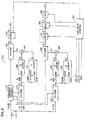
- Fig. 3 shows an implementation of the present invention in a signal processing ASIC, which is particularly useful in stand-alone satellite modems.
- the signal processing ASIC shown in Fig. 3 is formed on a substrate and includes a plurality of component circuits 121-128, a plurality of component routers 132-136, and a control processor interface 140 formed on the substrate. Additionally, the signal processing ASIC includes a timing generator 160 for generating internal clock enable signals for component circuits 121-128. The signal processing ASIC may optionally include phase detectors 170.
- Each of component circuits 121-128 performs a predetermined component function on a signal supplied thereto.
- component circuits 121 and 123 comprise input signal processing circuits for performing input signal processing on I and Q inputs, respectively.
- Component circuits 121 and 123 each include subcomponent circuits (151-154,155-158) comprising an input formatter (151,155), an input offsetter (152,156), an input scaler (153,157), and an input interpolator (154,155).
- Each of the subcomponents are connected to control processor interface 140 via a control processor (CP) bus 141.
- CP control processor
- Input formatters 151 and 155 receive data, which may be input in any of a number of possible formats, such as two's complement, offset binary, sign magnitude, two's complement negative, etc., and converts the input data into an internally used format.
- the data format is independently programmable for the various inputs to the signal processing ASIC. By selecting an internal format that is the same as the format of the input signal, input formatters 151 and 155 may be effectively bypassed.
- Input offsetters 152 and 156 permit the data supplied from input formatters 151 and 155 to be summed with an independently programmable DC offset.
- the offset may be selected to null out DC offsets from A/D converters. By selecting a zero offset, input offsetters 152 and 156 may be effectively bypassed.
- Input scalers 153 and 157 permit the data supplied from input offsetters 152 and 156 to be scaled by a right or left shift.
- the number of bits and the direction of shift may be independently programmed for each of input scalers 153 and 157. By selecting no shift, input scalers 152 and 156 may be effectively bypassed.
- Input interpolators 154 and 158 increase the sample rates of the input signals when the output signal is required to have a greater sample rate than the input signal. Basically, input interpolators 154 and 158 insert the appropriate number of zero-valued samples between input samples. When the input signals are interpolated, the rate of the internal clock driving the component circuits following input interpolators 154 and 158 is appropriately increased. The rate of interpolation may be implied from the ratio of two input clocks FIRCLX and INTCLK supplied to timing generator 160.
- Input interpolator 154 transmits an output signal designated as I DATA to component routers 132 and 133 for routing the I DATA output signal to either component circuit 124 or component circuit 125 for subsequent processing.
- input interpolator 158 transmits an output signal designated as Q DATA to component routers 133 and 134 for routing the I DATA output signal to either component circuit 125 or component circuit 126 for subsequent processing.
- the output of input interpolators 154 and 158 can be multiplied by a fixed number to adjust gain. This fixed number may be programmed independently on the I and Q data paths such that the gain is adjustable.
- Component circuit 124 comprises a finite input response (FIR) filter component including two subcomponents comprising a FIR input decimator/output interpolator 241 and a FIR filter 242.
- component circuit 126 comprises a finite input response (FIR) filter component including two subcomponents comprising a FIR input decimator/output interpolator 261 and a FIR filter 262.
- FIR finite input response
- component circuits 124 and 126 may be utilized to process I and Q data signals in parallel, or to provide a cascade filter for a data signal supplied to the input of component circuit 124.
- FIR filters 242 and 262 preferably operate by discrete time convolution of the input sequence with a stored sample impulse response.
- Exemplary FIR filters 242 and 262 receive control bits over CP bus 141 and select one of a number of predefined coefficients, which may be stored in a register, in response to the control bits. Additionally, FIR filters 242 and 262 preferably are capable of being internally cascaded to form a single filter of twice the length of either of FIR filters 242 and 262.
- FIR input decimators/output interpolators 241 and 261 may be utilized as either of an input decimator filter or an output interpolator. Because input decimator filters and output interpolators typically have identical construction and are not used simultaneously, the same structure may be utilized to perform both functions. As input decimator filters, FIR input decimators/output interpolators 241 and 261 digitally bandlimit the input sequence to minimize the alias fold-over phenomenon. As output interpolators, FIR input decimators/output interpolators 241 and 261 increase the sample rate at the output of the signal processing ASIC and perform true linear interpolation on output signals from FIR filters 242 and 262.
- Component circuit 124 provides an output signal to component router 135 and to component router 134 for routing back through component circuit 124 via component router 132, routing to component circuit 126, routing to component circuit 127, or for routing to circuit component 125 via routing component 133.
- Component circuit 126 provides an output signal to component router 134 and to component router 136 for routing back through component circuit 126, routing to component circuit 127, routing to component 128, or for routing to circuit component 125 via routing component 133.
- the significance of the routing path selected will be explained in more detail below.
- Component circuit 125 comprises a complex multiplier.
- the details of a complex multiplier 125 suitable for the signal processing ASIC is shown in Fig. 4.
- Complex multiplier 125 may receive inputs from numerous sources or combinations of sources. These sources include I and Q data lines, sine (SIN) and cosine (COS) data lines, and registers 431-434.
- Complex multiplier 125 may multiply the I data received on the I data line with the real part of a complex sinusoid supplied from component circuit 122 and multiply the Q data with the-imaginary part.
- the I and Q data are both multiplied by the SIN and COS outputs of component circuit 122, which comprises a numerically-controlled oscillator, using multipliers 411-414.
- the real portions of the multiplication product are added together by adder 441 to provide real output PI.
- the imaginary portions are added together by adder 441 to provide real output PQ.
- Adder 443 adds the real and imaginary portions together and outputs the result designated as PS.
- Complex multiplier 125 may also multiply the I and Q data by programmable constants stored in registers 431-434 to create a phase offset in a phase offset mode.
- register 431 controls multiplexers 421-424 such that coefficients RII, RIQ, RQI, and RQQ stored in registers 431-434 are supplied to multipliers 411-414 in place of the SIN and COS data.
- complex multiplier 125 transmits real output PI to component router 132 for routing to component circuit 124 and to component router 135 for routing to component circuit 127. Moreover, complex multiplier 125 transmits imaginary output PQ to component router 134 for routing to component circuit 126 and to component router 136 for routing to component circuit 128. The output sum of the real and imaginary portions PS is transmitted to component router 135 for routing to component circuit 127.
- Component circuit 122 comprises a numerically-controlled oscillator (NCO) including subcomponents comprising an infinite impulse response (IIR) filter 221, a phase accumulator 222, a phase-to-amplitude convertor 223, an I signal noise shaper 224, and a Q signal noise shaper 225.
- NCO 122 generates digital sinusoids by first accumulating the phase increment per clock cycle to form a phase ramp, and then converting the phase ramp to a corresponding quantized sinusoidal amplitude stored in a lookup table. Additionally, NCO 122 may perform post-processing on the quantized sinusoid to reduce quantization noise.
- IIR filter 221 is preferably a first order digital filter utilizing programmable coefficients and an output scaler. IIR filter 221 is of particular utility in applications such as phase locked loops, carrier recovery, and bit timing recovery loops.
- the output (IIR data) of IIR filter 221 is transmitted to phase accumulator 222.
- Phase accumulator 222 includes a bit shifter 510, an adder 515, a frequency A register 520, a frequency B register 521, a first multiplexer 525, a mode decoder and controller 530, an adder 535, a first register (A) 541, a second register (B) 542, a second multiplexer 545, an output register 550, an overflow detector 560, and a capture register 565.
- Phase accumulator 222 may be programmed via mode decoder and controller 530 to operate in a number of modes. These modes include (1) accumulate frequency A register 520, (2) accumulate frequency B register 521, (3) accumulate sum of frequency A register 520 and the IIR data, (4) switch between frequency A and B depending upon a status of an indicator pin, (5) accumulate separately frequency A register 520 and frequency B register 521 on alternate clock cycles, and (6) accumulate separately the sum of frequency A register 520 added to the IIR data and frequency B register 521 on alternate clock cycles.
- modes include (1) accumulate frequency A register 520, (2) accumulate frequency B register 521, (3) accumulate sum of frequency A register 520 and the IIR data, (4) switch between frequency A and B depending upon a status of an indicator pin, (5) accumulate separately frequency A register 520 and frequency B register 521 on alternate clock cycles, and (6) accumulate separately the sum of frequency A register 520 added to the IIR data and frequency B register 521 on alternate clock cycles.
- Bit shifter 510 shifts the bits of the IIR data supplied from IIR filter 221 in one bit increments.
- the shifted IIR data is sign extended to match the data length of frequency A and frequency B registers 520 and 521.
- Adder 515 adds the shifted IIR data to frequency A and transmits the sum to first multiplexer 525, overflow detector 560, and capture register 565.
- Overflow detector 560 detects an overflow resulting from the summation and issues an alarm if an overflow occurs.
- Capture register 565 stores the sum in real time.
- First multiplexer 525 selects either frequency A, frequency B, or the sum of frequency A and the IIR data in response to a mode designation signal from mode decoder and controller 530, and supplies the selected data to adder 535.
- Adder 535 adds the output of either register A 541 or register B 542 selected using multiplexer 545 depending upon the selected mode. Normally, the contents of register A 541 are added to the selected output of multiplexer 525 by adder 535. However, in the dual modes (5) and (6) above, the contents of register B 542 are also used on alternating clock cycles to permit simultaneous accumulation of two phases at half the clock rate.
- Phase-to-amplitude converter 223 includes a quadrant decoder 610, 1's complement converters 615 and 616, B lookup tables 620 and 622, N lookup tables 621 and 623, adders 631 and 632, 2's complement converters 635 and 636, output registers 641, 642, and 660, a dual mode controller 650, and a multiplexer 655.
- Phase-to-amplitude converter 223 is in essence a lookup table.
- Simplify lookup tables 620-623 store only the first quadrant of the sine function.
- the other quadrants of the sine function are generated by reversing the direction of the readout from lookup tables 620-623, by inverting the polarity of the output of lookup tables 620-623, or both.
- Reversing the direction of the readout can be accomplished by addressing lookup tables 620-623 with the 1's complement of the least significant bits of the input phase ramp received from phase accumulator 222.
- the polarity inversion is accomplished by taking the 2's complement of the output of the lookup tables 620-623.
- Quadrant decoder 610 The two most significant bits of the input received from phase accumulator 222 are supplied to quadrant decoder 610.
- Quadrant decoder 610 looks at these two most significant bits and determines which quadrant they represent.
- Quadrant decoder 610 then transmits separate instructions to 1's complement converters 615 and 616 to reverse the readout of lookup tables 620-623 depending upon the detected quadrant.
- quadrant decoder 610 then transmits separate instructions to 2's complement converters 635 and 636 to perform polarity inversion by taking the two's complement of the outputs lookup tables 620-623 depending upon the detected quadrant.
- Table 1 shows an example of how quadrant decoder determines the quadrant from the two most significant bits of the input signal. TABLE 1 Quadrant MSBs Cosine Polarity Sine Polarity Cosine Direction Sine Direction 0 00 + + reverse forward 1 01 - + forward reverse 2 10 - - reverse forward 3 11 + - forward reverse
- B lookup tables 620 and 622 are used to look up the sin ⁇ 1 portions of the above equation and N lookup tables 621 and 623 are used to lookup the sin ⁇ 2cos ⁇ 1 portions.
- Adder 631 adds the outputs of B lookup table 620 and N lookup table 622 to provide the approximation sin ⁇ .
- adder 632 adds the outputs of B lookup table 621 and N lookup table 623 to provide the approximation sin ⁇ , which is converted to cos ⁇ by appropriate inversion performed using 1's complement converter 616 under instruction of quadrant decoder 610.
- 1's complement converters 615 and 616 supply the ten most significant of the remaining bits, which represent ⁇ 1, to B lookup tables 620 and 622 and supply the five most significant of the remaining bits (the five most significant bits of ⁇ 1), which represent ⁇ 1, to a cosine input of N lookup tables 621 and 623 and the five least significant of the remaining bits, which represent ⁇ 2, to the sine input of N lookup tables 621 and 623.
- the output of 2's complement converter 635 is provided to output register 640 for subsequent transmission to Q noise shaper 225.
- the output of 2's complement converter 636 is provided to output register 641 and multiplexer 655.
- Output register 641 provides an output to multiplexer 655.
- Multiplexer 655 permits register 641 to be bypassed depending upon whether NCO 122 is operating in a dual mode.
- Multiplexer 655 provides an output to output register 660 for subsequent transmission to I signal noise shaper 224.
- Dual mode controller 650 receives mode designation signals from mode decoder and controller 530 (Fig. 5) of phase accumulator 222 and controls phase-to-amplitude converter 223 to output a sine output, a cosine output, or to operate in a dual mode.
- I signal noise shaper 224 and Q signal noise shaper 225 are provided to reduce amplitude quantization noise.
- I signal noise shaper 224 and Q signal noise shaper 225 preferably quantize the input data received from phase-to-amplitude converter 223, filter the differences between the quantized data and the input data, and subtract this filtered difference from the input data.
- I signal noise shaper 224 provides an output signal, which is designated as NCO C in Fig. 3, to component router 132 for subsequent routing to component circuit 124, to the COS input of component circuit 125, and to component router 135 for subsequent routing to component circuit 127.
- Q signal noise-shaper 225 provides an output signal, which is designated as NCO S in Fig. 3, to component router 134 for subsequent routing to component circuit 126, to the SIN input of component circuit 125, and to component router 136 for subsequent routing to component circuit 128.
- Component circuits 127 and 128 comprise signal processing circuits for performing output signal processing on I and Q data respectively supplied thereto.
- Component circuits 127 and 128 each include subcomponent circuits (271-274,281-284) comprising an output decimator (271,281), an output scaler (272,282), an output offsetter (273,283), and an output formatter (274,284).
- Each of the subcomponents are connected to control processor interface 140 via a control processor (CP) bus 141.
- CP control processor
- Output decimators 271 and 272 may be independently instructed to reduce the sample rates of the data signals supplied from component routers 135 and 136, respectively.
- Output scalers 272 and 282 permit the data supplied from output decimators 271 and 281 to be scaled by a right or left shift.
- a right shift rounds up the data to be output and reduces truncation errors.
- the number of bits and the direction of shift may be independently programmed for each of output scalers 272 and 282. By selecting no shift, output scalers 272 and 282 may be effectively bypassed.
- Output offsetters 273 and 283 permit the data supplied from output scalers 272 and 274 to be summed with an independently programmable DC offset.
- the offset may be selected to null out DC offsets from D/A converters. By selecting a zero offset, output offsetters 273 and 283 may be effectively bypassed.
- Output formatters 274 and 284 receive processed data, which may have been processed in number of possible formats, such as two's complement, offset binary, sign magnitude, two's complement negative, etc., from output offsetters 273 and 274 and converts the processed data into a desired format for subsequent use.
- the output data format is independently programmable. By selecting an internal format that is the same as the format of the output signal, output formatters 274 and 284 may be effectively bypassed.
- Output formatter 274 provides the I output (I OUT) of the signal processing ASIC, while output formatter 284 provides the Q output (Q OUT).
- Component routers 132-136 selectively couple together component circuits 121-128 to selectively route signals therethrough.
- Component router 132 includes three multiplexers, each of which is connected to CP bus 141 and controlled by control processor interface 140.
- a first multiplexer 321 receives outputs I DATA, NCO C, and CM PI from input interpolator 154, I signal noise shaper 224, and complex multiplier 125, respectively, and supplies one of these outputs to second multiplexer 322 and third multiplexer 323.
- Second multiplexer 322 selects the output provided by first multiplexer 321 or the output from FIR filter 242, and provides the selected output to FIR input decimator/output interpolator 241.
- Third multiplexer 323 selects the output provided by first multiplexer 321 or the output from FIR input decimator/output interpolator 241, and provides the selected output to FIR filter 242.
- Component router 133 includes two multiplexers, each of which is connected to CP bus 141 and controlled by control processor interface 140.
- a first multiplexer 331 receives outputs I DATA and I FD from input interpolator 154 and component router 135, respectively, and supplies a selected one of these outputs to the I input of complex multiplier 125.
- a second multiplexer 332 receives outputs I DATA, Q DATA, and I FD from input interpolator 154, input interpolator 158, and component router 135, respectively, and supplies a selected one of these outputs to the Q input of complex multiplier 125.
- Component router 134 includes three multiplexers, each of which is connected to CP bus 141 and controlled by control processor interface 140.
- a first multiplexer 341 receives outputs Q DATA, NCO S, CM PQ, and I FD from input interpolator 158, Q signal noise shaper 225, complex multiplier 125, and component router 135, respectively, and supplies one of these outputs to second multiplexer 342 and third multiplexer 343.
- Second multiplexer 342 selects the output provided by first multiplexer 341, the output from FIR filter 262, or the output provided by FIR filter 242 and provides the selected output to FIR input decimator/output interpolator 261.
- Third multiplexer 343 selects the output provided by first multiplexer 341 or the output from FIR input decimator/output interpolator 261, and provides the selected output to FIR filter 262.
- Component router 135 includes two multiplexers, each of which is connected to CP bus 141 and controlled by control processor interface 140.
- a first multiplexer 351 selects the output provided by FIR filter 242 or FIR input decimator/output interpolator 241 and provides the selected output, which is designated as I FD, to the input of a second multiplexer 352 of component router 135, first multiplexer 331 of component router 133, and first multiplexer 341 of component router 134.
- Second multiplexer 352 receives outputs I FD, NCO C, CM PI, CM PS, and Q SR from first multiplexer 351, I signal noise shaper 224, the PI and PS outputs of complex multiplier 125, and FIR filter 262, respectively, and selects one of these outputs to supply to output decimator 271.
- Component router 136 includes two multiplexers, each of which is connected to CP bus 141 and controlled by control processor interface 140.
- a first multiplexer 361 selects the output provided by FIR filter 262 or FIR input decimator/output interpolator 261 and provides the selected output, which is designated as Q FD, to the input of a second multiplexer 362 of component router 136 and second multiplexer 332 of component router 133.
- Second multiplexer 362 receives outputs Q FD, NCO S, and CM PQ from first multiplexer 361, Q signal noise shaper 225, and the PQ output of complex multiplier 125, respectively, and selects one of these outputs to supply to output decimator 281.
- Control processor interface 140 receives control signals from an external source and controls component routers 132-136 such that selected component circuits 121-128 are coupled together in a manner by which the predetermined component functions of selected component circuits 121-128 are performed on input signals in an order necessary to accomplish a selected programmable function for the signal processing ASIC.
- the signal processing ASIC operates in one of the following modes to perform the corresponding function:
- I and Q input data is passed through input processors 121 and 122 to component routers 132 and 134, respectively.
- Component routers 132 and 134 route the data to FIR filters 242 and 262 when no input decimation is desired, and route the data through FIR input decimators/output interpolators 241 and 261 when input decimation is desired.
- component routers 132 and 134 subsequently route the outputs of FIR input decimators/output interpolators 241 and 261 to FIR filters 242 and 262.
- Component routers 135 and 136 route the outputs of FIR filters 242 and 262 to component router 133 when output interpolation is not desired.
- component routers 132 and 134 route the output of FIR filters 242 and 262 through FIR input decimators/output interpolators 241 and 261, and then the outputs of FIR input decimators/output interpolators 241 and 261 are then routed to component router 133.
- Component router 133 routes these outputs to the I and Q inputs of complex multiplier 125.
- Complex multiplier 125 multiplies the I and Q data with phase offset coefficients stored in registers 431-434.
- Component routers 135 and 136 then route the PI and PQ outputs of complex multiplier 125 to output processors 127 and 128.
- component router 132 In the cascaded baseband filtering mode, only the I data input is used. Data from this input passes through input processor 121 and is provided to component router 132. Component router 132 routes the data to FIR filter 242 when no input decimation is desired, and routes the data through FIR input decimator/output interpolator 241 when input decimation is desired. When the data is first sent to FIR input decimator/output interpolator 241, component router 132 subsequently routes the output of FIR input decimator/output interpolator 241 to FIR filter 242. The output of FIR filter 242 is provided to component router 134, which routes the output to FIR filter 262.
- Component router 134 routes the output of FIR filter 262 to component router 136 when no output interpolation is desired, and routes the output through FIR input decimator/output interpolator 261 when output interpolation is desired. Whenever the output of FIR filter 262 is first sent to FIR input decimator/output interpolator 261, component router 134 subsequently routes the output of FIR input decimator/output interpolator 261 to FIR filter 262. The output of FIR filter 262 is provided to component router 136, which routes the output to output processor 128.
- the signal processing ASIC operates in much the same manner as in the dual baseband filtering mode described above, with the following exceptions.
- NCO 122 is utilized to provide inputs directly to the SIN and COS inputs of complex multiplier 125.
- the PS output of complex multiplier 125 is routed through output processor 127 to the I output by component router 135.
- the resulting output is a digital representation of a quadrature modulated carrier.
- I and Q input data is passed through input processors 121 and 122 to component routers 133, which passes the I and Q data to the respective I and Q inputs of complex multiplier 124.
- Complex multiplier 125 multiplies the I and Q data with SIN and COS data supplied to the SIN and COS inputs of complex multiplier 125 by NCO 122.
- Component routers 132 and 134 then route the PI and PQ outputs of complex multiplier 125 to FIR filters 242 and 262 when no input decimation is desired, and route the PI and PQ outputs through FIR input decimators/output interpolators 241 and 261 when input decimation is desired.
- component routers 132 and 134 subsequently route the outputs of FIR input decimators/output interpolators 241 and 261 to FIR filters 242 and 262.
- Component routers 135 and 136 route the outputs of FIR filters 242 and 262 to component routers 135 and 136 when output interpolation is not desired.
- component routers 132 and 134 route the output of FIR filters 242 and 262 through FIR input decimators/output interpolators 241 and 261, and then the outputs of FIR input decimators/output interpolators 241 and 261 are then routed to component routers 135 and 136, which route the outputs to output processors 127 and 128.
- the complex multiplier an NCO are used as a phase rotator in a carrier recovery loop.
- the signal processing ASIC operates in much the same manner as in the baseband quadrature demodulation and baseband filtering mode described above, with the exception that only the I input port is used.
- the I DATA from input processor 121 is supplied to both the I and Q input terminals of complex multiplier 125.
- the I DATA represents sampled IF data and NCO 122 is used as both a downconverter to baseband and a phase rotator.
- Phase accumulator 222 may offset the output of IIR filter 221 by a fixed frequency (A or B) in this mode, with the fixed frequency representing the carrier frequency.
- the COS and SIN outputs of NCO 122 are passed to output processors 127 and 128, respectively, by component routers 135 and 136.
- noise shaping may be independently enabled or disabled and the frequency may be programmed to frequency A or B.
- the component routers route the output of NCO 122 in the same manner as in the stand-alone quadrature mode.
- NCO operates in a dual mode and the cosine of the frequency programmed into frequency A register 520 emerges from the I output port while the sine of the frequency programmed into frequency B register 521 emerges from the Q output port.
- frequency A added to the output of IIR filter 221 can also be programmed to emerge from the I output port.
- noise shaping by signal noise shapers 224 and 225 may be independently enabled or disabled and a finite state machine (not shown) may be used to control the component routers.
- the component routers route the data in much the same manner as in the cascade baseband filtering mode.
- I and Q shift registers (not shown) in FIR filters 242 and 262 effectively form one double-length shift register.
- a partial sum input is added to the output of FIR filter 242; and the output of FIR filter 242 is added to the output of FIR filter 262.
- FIR filters 242 and 262 each have shift register inputs and outputs and partial sum inputs and outputs.
- the shift register input of the first stage is connected to the data source via I input port and the partial sum input of the first stage is connected to ground via Q input port.
- the shift register output of the first stage is connected to the shift register input of the next stage and the partial sum output of the first stage is connected to the partial sum input of the next stage.
- the signal processing ASIC operates in much the same manner as in the baseband filtering and quadrature modulation mode described above, with the following exceptions.
- complex multiplier 125 multiplies the outputs of output interpolators 241 and 261 with the outputs of NCO 122 and outputs are provided from the PI and PQ outputs of complex multiplier 125 via the I and Q.
Landscapes
- Engineering & Computer Science (AREA)
- Physics & Mathematics (AREA)
- Theoretical Computer Science (AREA)
- General Physics & Mathematics (AREA)
- Data Mining & Analysis (AREA)
- General Engineering & Computer Science (AREA)
- Computer Hardware Design (AREA)
- Mathematical Physics (AREA)
- Algebra (AREA)
- Computational Mathematics (AREA)
- Mathematical Analysis (AREA)
- Mathematical Optimization (AREA)
- Pure & Applied Mathematics (AREA)
- Databases & Information Systems (AREA)
- Software Systems (AREA)
- Digital Transmission Methods That Use Modulated Carrier Waves (AREA)
- Radio Relay Systems (AREA)
Applications Claiming Priority (2)
| Application Number | Priority Date | Filing Date | Title |
|---|---|---|---|
| US268938 | 1988-11-07 | ||
| US08/268,938 US5793656A (en) | 1994-06-30 | 1994-06-30 | Application-specific integrated circuits having programming functions |
Publications (1)
| Publication Number | Publication Date |
|---|---|
| EP0690391A1 true EP0690391A1 (fr) | 1996-01-03 |
Family
ID=23025156
Family Applications (1)
| Application Number | Title | Priority Date | Filing Date |
|---|---|---|---|
| EP95850126A Withdrawn EP0690391A1 (fr) | 1994-06-30 | 1995-06-30 | Circuit intégré d'application spécifique comprenant des fonctions programmables |
Country Status (3)
| Country | Link |
|---|---|
| US (1) | US5793656A (fr) |
| EP (1) | EP0690391A1 (fr) |
| CA (1) | CA2153127C (fr) |
Families Citing this family (8)
| Publication number | Priority date | Publication date | Assignee | Title |
|---|---|---|---|---|
| FR2776093A1 (fr) * | 1998-03-10 | 1999-09-17 | Philips Electronics Nv | Circuit processeur programmable muni d'une memoire reconfigurable, pour realiser un filtre numerique |
| JP4147607B2 (ja) * | 1998-03-13 | 2008-09-10 | 松下電器産業株式会社 | 補助スクランブル/デスクランブル方法および装置 |
| JP4722266B2 (ja) * | 2000-08-16 | 2011-07-13 | 富士通セミコンダクター株式会社 | オーバサンプリングfirフィルタ、オーバサンプリングfirフィルタの制御方法、およびオーバサンプリングfirフィルタを有する半導体集積回路、オーバサンプリングfirフィルタでフィルタリングされたデータを送信する通信システム |
| US7062635B2 (en) * | 2002-08-20 | 2006-06-13 | Texas Instruments Incorporated | Processor system and method providing data to selected sub-units in a processor functional unit |
| US20060012714A1 (en) * | 2004-07-16 | 2006-01-19 | Greenforest Consulting, Inc | Dual-scaler architecture for reducing video processing requirements |
| KR100673406B1 (ko) * | 2005-01-26 | 2007-01-24 | 아태위성산업 주식회사 | 지상 휴대전화기에 탑재되는 위성 통신 장치 및 방법 |
| US7629998B2 (en) * | 2005-06-23 | 2009-12-08 | Elbex Video Limited | Method and apparatus for measuring illumination and camera performances |
| US7917798B2 (en) | 2005-10-04 | 2011-03-29 | Hypres, Inc. | Superconducting digital phase rotator |
Citations (2)
| Publication number | Priority date | Publication date | Assignee | Title |
|---|---|---|---|---|
| US4694416A (en) * | 1985-02-25 | 1987-09-15 | General Electric Company | VLSI programmable digital signal processor |
| EP0509376A2 (fr) * | 1991-04-17 | 1992-10-21 | Hitachi, Ltd. | Dispositif de traitement de signaux |
Family Cites Families (5)
| Publication number | Priority date | Publication date | Assignee | Title |
|---|---|---|---|---|
| CA1265255A (fr) * | 1986-07-31 | 1990-01-30 | John Polkinghorne | Circuit integre pour usage specifique |
| JPH01226066A (ja) * | 1988-03-04 | 1989-09-08 | Hitachi Ltd | ディジタル信号処理プロセッサ |
| GB2259377B (en) * | 1991-08-08 | 1995-06-21 | British Aerospace Space & Comm | Multi-function application specific integrated circuit for controlling spacecraft thrusters |
| US5418911A (en) * | 1992-06-09 | 1995-05-23 | Intel Corporation | Data path switch method and apparatus that provides capacitive load isolation |
| US5311459A (en) * | 1992-09-17 | 1994-05-10 | Eastman Kodak Company | Selectively configurable integrated circuit device for performing multiple digital signal processing functions |
-
1994
- 1994-06-30 US US08/268,938 patent/US5793656A/en not_active Expired - Lifetime
-
1995
- 1995-06-30 EP EP95850126A patent/EP0690391A1/fr not_active Withdrawn
- 1995-06-30 CA CA002153127A patent/CA2153127C/fr not_active Expired - Fee Related
Patent Citations (2)
| Publication number | Priority date | Publication date | Assignee | Title |
|---|---|---|---|---|
| US4694416A (en) * | 1985-02-25 | 1987-09-15 | General Electric Company | VLSI programmable digital signal processor |
| EP0509376A2 (fr) * | 1991-04-17 | 1992-10-21 | Hitachi, Ltd. | Dispositif de traitement de signaux |
Non-Patent Citations (4)
| Title |
|---|
| BROWN A: "APPLICATION SPECIFIC DIGITAL SIGNAL PROCESSING", ELECTRONICS WORLD AND WIRELESS WORLD, vol. 99, no. 1688, 1 July 1993 (1993-07-01), pages 581 - 583, XP000378446 * |
| FELLMAN R D: "DESIGN ISSUES AND AN ARCHITECTURE FOR THE MONOLITHIC IMPLEMENTATION OF A PARALLEL DIGITAL SIGNAL PROCESSOR", IEEE TRANSACTIONS ON ACOUSTICS,SPEECH AND SIGNAL PROCESSING, vol. 38, no. 5, 1 May 1990 (1990-05-01), pages 839 - 852, XP000128651 * |
| HAMILTON B: "PROGRAMMABLE ARCHITECTURE FOR MATRIX AND SIGNAL PROCESSING", SPANNING THE PEAKS OF ELECTROTECHNOLOGY, COLORADO SPRINGS, MAR. 21 - 23, 1988, 21 March 1988 (1988-03-21), INSTITUTE OF ELECTRICAL AND ELECTRONICS ENGINEERS, pages 116 - 120, XP000118348 * |
| R. CROCHIERE AND R. RABINER: "multirate digital signal processing", PRENTICE-HALL, US, 014080 * |
Also Published As
| Publication number | Publication date |
|---|---|
| CA2153127A1 (fr) | 1995-12-31 |
| CA2153127C (fr) | 1999-05-04 |
| US5793656A (en) | 1998-08-11 |
Similar Documents
| Publication | Publication Date | Title |
|---|---|---|
| KR100373525B1 (ko) | 고정된샘플링레이트를사용한이산시간샘플시스템들을위한가변레이트다운샘플링필터장치및그방법 | |
| KR0130471B1 (ko) | Ssb 신호 발생기 | |
| US5764113A (en) | Re-sampling circuit and modulator using same | |
| HUT68003A (en) | Psk demodulator | |
| AU732601B2 (en) | Sample rate converter | |
| AU573966B2 (en) | Zero-if digital receiver | |
| US5793656A (en) | Application-specific integrated circuits having programming functions | |
| WO2001013562A2 (fr) | Architecture de demodulateur numerique en rafale grande vitesse | |
| JPH06133273A (ja) | Qam信号処理装置 | |
| US5712879A (en) | Differential detecting device | |
| CA2094672C (fr) | Oscillateur numerique | |
| WO1999019812A1 (fr) | Filtre numerique a reponse impulsionnelle infinie reconfigurable | |
| EP0535591B1 (fr) | Circuit d'asservissement de phase capable d'être mise rapidement en un état d'asservissement | |
| EP0481543A1 (fr) | Arrangement de filtrage | |
| EP0535638A2 (fr) | Diviseur de phase pour signaux complexes | |
| JP3191895B2 (ja) | Ssb変調器 | |
| EP1158674A2 (fr) | Filtre numérique pour générer des signaux IQ, formeur de bruit et circuit pour supprimer des canaux adjacents | |
| GB2231224A (en) | Hue control circuits | |
| EP0488624B1 (fr) | Un circuit numérique de détection de phase en quadrature | |
| US6324222B1 (en) | Digital receiver with polyphase structure | |
| JP3415653B2 (ja) | ディジタル変復調器 | |
| JPH0669969A (ja) | 4相位相変調器 | |
| AU716743B2 (en) | PSK demodulator | |
| JP3177266B2 (ja) | デジタル変調信号復調回路 | |
| JPH05248890A (ja) | エンコーダ信号逓倍回路 |
Legal Events
| Date | Code | Title | Description |
|---|---|---|---|
| PUAI | Public reference made under article 153(3) epc to a published international application that has entered the european phase |
Free format text: ORIGINAL CODE: 0009012 |
|
| AK | Designated contracting states |
Kind code of ref document: A1 Designated state(s): DE ES FR GB IT SE |
|
| 17P | Request for examination filed |
Effective date: 19960703 |
|
| RAP1 | Party data changed (applicant data changed or rights of an application transferred) |
Owner name: HE HOLDINGS, INC. |
|
| RAP1 | Party data changed (applicant data changed or rights of an application transferred) |
Owner name: HUGHES ELECTRONICS CORPORATION |
|
| STAA | Information on the status of an ep patent application or granted ep patent |
Free format text: STATUS: THE APPLICATION IS DEEMED TO BE WITHDRAWN |
|
| 18D | Application deemed to be withdrawn |
Effective date: 20030103 |