EP0691683A2 - Schutzstruktur für ingegrierte Schaltungen - Google Patents
Schutzstruktur für ingegrierte Schaltungen Download PDFInfo
- Publication number
- EP0691683A2 EP0691683A2 EP95110474A EP95110474A EP0691683A2 EP 0691683 A2 EP0691683 A2 EP 0691683A2 EP 95110474 A EP95110474 A EP 95110474A EP 95110474 A EP95110474 A EP 95110474A EP 0691683 A2 EP0691683 A2 EP 0691683A2
- Authority
- EP
- European Patent Office
- Prior art keywords
- zone
- drain
- connection
- protective structure
- resistance
- Prior art date
- Legal status (The legal status is an assumption and is not a legal conclusion. Google has not performed a legal analysis and makes no representation as to the accuracy of the status listed.)
- Granted
Links
Images

Classifications
-
- H—ELECTRICITY
- H10—SEMICONDUCTOR DEVICES; ELECTRIC SOLID-STATE DEVICES NOT OTHERWISE PROVIDED FOR
- H10D—INORGANIC ELECTRIC SEMICONDUCTOR DEVICES
- H10D89/00—Aspects of integrated devices not covered by groups H10D84/00 - H10D88/00
- H10D89/60—Integrated devices comprising arrangements for electrical or thermal protection, e.g. protection circuits against electrostatic discharge [ESD]
- H10D89/601—Integrated devices comprising arrangements for electrical or thermal protection, e.g. protection circuits against electrostatic discharge [ESD] for devices having insulated gate electrodes, e.g. for IGFETs or IGBTs
- H10D89/911—Integrated devices comprising arrangements for electrical or thermal protection, e.g. protection circuits against electrostatic discharge [ESD] for devices having insulated gate electrodes, e.g. for IGFETs or IGBTs using passive elements as protective elements
-
- H—ELECTRICITY
- H10—SEMICONDUCTOR DEVICES; ELECTRIC SOLID-STATE DEVICES NOT OTHERWISE PROVIDED FOR
- H10D—INORGANIC ELECTRIC SEMICONDUCTOR DEVICES
- H10D89/00—Aspects of integrated devices not covered by groups H10D84/00 - H10D88/00
- H10D89/60—Integrated devices comprising arrangements for electrical or thermal protection, e.g. protection circuits against electrostatic discharge [ESD]
- H10D89/601—Integrated devices comprising arrangements for electrical or thermal protection, e.g. protection circuits against electrostatic discharge [ESD] for devices having insulated gate electrodes, e.g. for IGFETs or IGBTs
Definitions
- the invention relates to a protective structure for protecting an output or input of an integrated circuit (IC) against overvoltages with an n-channel MOS field-effect transistor (transistor).
- IC integrated circuit
- transistor n-channel MOS field-effect transistor
- Such a protective structure serves to protect the IC against electrostatic discharge currents that can reach the pins of the IC.
- discharge currents can reach the pins, for example, when handling the IC due to discharges of electrically charged bodies, for example by a person, by metal tools, by a housing, etc.
- the object of the invention is to improve the protective structure in such a way that the bipolar state of the transistor is more stable and the transition to the bipolar state is nevertheless rapid.
- drain zone and the Drain connection zone are spatially separated from each other, and that in the substrate below the drain zone and the drain connection zone an n-doped resistance zone with weaker doping than the doping of the drain zone and the drain connection zone is formed such that it is the electrically conductive connection between the drain zone and the Drain connection zone forms.
- the drain-gate edge as in conventional n-channel MOS transistors, consists of a flat, highly doped pn junction. This ensures a low termination voltage for the transition to bipolar operation, i.e. for the snap-back process, which is therefore quick. Because of the n-doped resistance zone arranged according to the invention, this weakly doped resistance zone extends near the drain edge further into the interior of the substrate body. This avoids the risk of thermal overload during the transition to the bipolar state. This can be explained by the fact that, at the termination voltage, current constrictions occur at the pn junction, which are now distributed along the drain / gate edge.
- Thermal interference effects due to the metal connection contacts in the drain connection zone on the drain zone and thus on the mode of operation of the transistor are also prevented. Because of the resistance zone there is a large distance between the drain / gate edge and the connection contacts, so that the heat conduction to the connection contacts takes place over a longer distance. Because of the arrangement according to the invention, there is an n-zone doped according to the resistance zone between the drain zone and the drain-connection zone on the surface of the substrate body, which is not bridged with the n-doping of the drain zone and the drain-connection zone. The drain zone and the drain connection zone can have the same n-doping.
- n-channel transistor can be produced without additional steps and without additional masks in the normal MOS process for producing the IC.
- the resistance zone extends at most up to the gate / drain edge of the drain zone. This results in a good coupling of the resistance zone to the drain zone.
- the largest possible area of the drain zone can be covered, which is limited in that the size of the channel formed below the gate electrode between the source zone and the drain zone is not impaired.
- the resistance zone advantageously extends below the entire drain connection zone, so that good contact between the resistance zone and the drain connection zone is ensured.
- the width of the resistance zone is advantageously more than 10 ⁇ m, preferably 100 ⁇ m. This is a convenient size for the usual dimensions of MOS n-channel transistors of high power and thus small dimensions.
- the width of the resistance zone is then somewhat larger than the width of the transistor. It is advantageous to use the n-well of the CMOS process as a resistance zone.
- the depth of the resistance zone is significantly greater than the depth of the drain zone or the drain connection zone, in particular by a factor of 3 to 5.
- the depth can be selected in accordance with the desired function of the individual transistor. A significantly larger factor of 1.5 can also be understood.
- an n-zone with weaker doping than the doping of the source zone can be formed below the source zone. This also prevents the occurrence of electrical short circuits due to alloy effects due to the metallic electrode connections.
- the drain region can also be connected via a connection directly to an input element, in particular a gate electrode, of an input transistor of the IC to be protected.
- the protective function against electrostatic charging caused by the arrangement of the transistor according to the invention also acts on transistors with a very small depth of the source and drain connections which are used in fast circuits.
- Such transistors can also be successfully implemented and used in siliconized techniques. This applies both if only one of the gate, source or Drain zones or all are siliconized.
- a transistor designed according to the invention is particularly advantageous. Siliconized zones are very low-resistance, and normally such transistors are particularly at risk in electrostatic conditions.
- the protective effect of the resistance zone is particularly important here.
- the transistor according to the invention can be used to protect the output of an IC. It can then form the output stage of the IC itself, so that no separate component is required for the protective device. This can save space in chip technology.
- the transistor according to the invention is used e.g. as an open drain output, as part of a push-pull stage and is also used in combined outputs and inputs in CMOS technology.
- the drain zone of the protective structure is connected via its connection to an input element, e.g. connected to a gate electrode of a transistor.
- the gate electrode is placed on the source potential, for which the ground potential is usually used.
- the protective structure according to the invention is also used between supply lines, in particular the positive supply line and the ground, of an IC or a partial circuit of an IC.
- a drain zone 2 and a source zone 3 are formed on a p-doped substrate body 1 for each of the two n-channel transistors. Furthermore, a drain connection zone 4 is provided which is arranged separately from the drain zones 2 and which is used jointly for both transistors. On the drain connection zone 4 are how to 1, drain connections 5 are provided for both transistors. The source connections 6 are provided on the respective source zone 3 of the two transistors. A gate electrode 7 is provided on an insulating layer 8 between the drain zone 2 and the source zone 3 of the transistors. A field oxide layer is arranged between the drain zone 2 and the drain connection zone 4, which isolates the drain zone 2 from the drain connection zone 4. The arrangement of the two transistors is mirror-symmetrical to the axis of symmetry A. To make contact with the drain connections 5 and the source connections 6, conductor tracks 15 and 16, which typically consist of aluminum and one, are applied to the drain and source regions Make contact connection (pad).
- n-well 10 is provided below the drain zones 2 and the drain connection zones 4, which has a lower doping than the drain zones 2 and the drain connection zones 4. Since the drain zones 2 are insulated from one another by the drain connection zones 4 by means of the field oxide layers 9, the electrical conduction takes place between the drain zones 2 and the drain connection zone 4 via the n well 10.
- the n well 10 extends below the entire drain connection zone 4 and up to the vicinity of the gate / drain edge of the drain zones 2. This ensures good contact between the n-well 10 and the drain zones 2 and the drain connection zones 4.
- the n-well 10 does not extend all the way to the gate / drain edge, so that the channel 11 between the respective drain zone and the respective source zone 3 of a transistor does not pass below the gate electrode 7 through the n - tub is narrowed.
- the n-well 10 is also designed such that it extends into the substrate body 1 by a multiple of the depth of the drain zones 2, so that the pn junction is thereby moved further into the interior of the substrate body. This creates a deeper but weaker doped pn junction than that between the drain zone 2 and the channel zone 11.
- the protective arrangement is connected to an input element of the IC, e.g. connected to a gate electrode of an input transistor.
- the protective structure 17 shows the transistor 18 to which the resistor formed by the resistance zone 10 is connected in series.
- the interconnect 15 connected to the drain connection zone leads to an outer connection pad 19 which the IC can be connected to external connections.
- the transistor 18 is connected as a diode, the conductor track 16 from the source connections and the gate electrode 7 being connected to a fixed potential, preferably to ground.
- the drain region of the transistor 18 is connected at its connection 12 to an input element 21 of the IC, ie the inner part of the IC.
- the input element is a CMOS inverter stage.
- the protective structure 17 is used here as part of a push-pull output stage 22 of an IC.
- the protective structure 17 consists of a plurality of transistors 18 connected in parallel with each other, to the drain of which a resistor formed by the resistance region 10 is connected in series.
- the drain terminal 15 leads to a connection pad 19, which is an input / output connection pad.
- the transistors 18 connected in parallel with their resistance regions 10 correspond to a protective structure as shown in FIG. 1 with a plurality of connections connected in parallel.
- the connection 12 of the drain regions of the protective structure 17 leads via a resistor 20 to an input 23 of the inner part of the IC.
- the gate electrodes are driven by a signal line 24 coming from the inner part 27 of the IC.
- the gate electrodes of the p-channel transistors 25, which form the second branch of the push-pull stage, are likewise driven by a signal line 26, which likewise comes from the inner part 27 of the IC.
- the W / L ratio of the transistors 25 of the second branch is significantly larger than the W / L ratio of the transistors 18 of the first branch of the push-pull stage.
- the mode of operation of the transistor arrangement according to the invention is described below. If a positive voltage pulse reaches, for example, an external connection of the IC to the drain connection zone connected to this connection, the n-channel MOS transistor changes into a bipolar operating state when the drain-source or drain-substrate termination voltage is reached. This operating state is also referred to as the npn state.
- the conductor tracks 16 are typically connected to ground.
- the n-well 10 forms a series resistance between the drain zone 2 and the drain connection zone 4. Furthermore, it forms a pn junction between the drain zone 2 and the channel 11, which extends deep into the substrate body 1 Collector pn transition.
- the transistor Due to the series resistance of this n-well, constrictions in the current occurring at the pn junction are prevented during the transition to the pn state.
- the transistor can take up more power in the bipolar state than with conventional arrangements. By connecting two or more transistors in parallel, the current that occurs is distributed even further, so that the power can be absorbed by both transistors, since the power loss is distributed over an even larger area.
Landscapes
- Metal-Oxide And Bipolar Metal-Oxide Semiconductor Integrated Circuits (AREA)
- Insulated Gate Type Field-Effect Transistor (AREA)
- Semiconductor Integrated Circuits (AREA)
Abstract
Description
- Die Erfindung betrifft eine Schutzstruktur zum Schutz eines Ausgangs oder Eingangs einer integrierten Schaltung (IC) gegen Überspannungen mit einem n-Kanal-MOS-Feldeffekt-Transistor (Transistor).
- Eine solche Schutzstruktur dient dazu, das IC gegen elektrostatische Entladungsströme zu schützen, die auf Pins des IC's gelangen können. Solche Entladungsströme können beispielsweise beim Handhaben des IC's aufgrund von Entladungen elektrisch aufgeladener Körper, beispielsweise durch einen Menschen, durch Metallwerkzeuge, durch ein Gehäuse etc. auf die Pins gelangen.
- Aus EOS/ESD Symposium Proceedings 1991, S.88, Charvaka Duvvury und Robert Rountree ist eine Schutzanordnung für integrierte Schaltungen (IC) mit einem n-Kanal-MOS-Feldeffekt-Transistor (Transistor) bekannt, die gegen elektrostatische Überlastung von Eingängen oder Ausgängen vorgesehen ist. Hierzu wird der mit dem Pin, d.h. mit dem entsprechenden Ausgang oder Eingang, verbundene Transistor, der stets einen parasitären Bipolar-Transistor enthält, in den Bipolar-Zustand gebracht, in welchem er mit hohem Strom bei einer niedrigeren Spannung betrieben werden kann. Dieser Vorgang wird als "snap-back" bezeichnet. Aufgrund der Erniedrigung der Spannung infolge des Bipolarbetriebs kann der Transistor mehr Leistung aufnehmen. Zum weiteren Schutz des Transistors soll der Übergang in den Bipolarzustand möglichst schnell erfolgen und der Bipolarzustand soll möglichst stabil gehalten werden, da ein zweites "snap-back", der "second breakdown" des Bipolartransistors, diesen zerstören würde.
- Der Erfindung liegt die Aufgabe zugrunde, die Schutzstruktur dahingehend zu verbessern, daß der Bipolarzustand des Transistors stabiler ist und der Übergang in den Bipolarzustand trotzdem schnell erfolgt.
- Dies wird erfindungsgemäß dadurch erreicht, daß die Drainzone und die Drainanschlußzone räumlich getrennt voneinander angeordnet sind, und daß im Substrat unterhalb der Drainzone und der Drainanschlußzone eine n-dotierter Widerstandszone mit schwächerer Dotierung als die Dotierung der Drainzone und der Drainanschlußzone derart ausgebildet ist, daß sie die elektrisch leitende Verbindung zwischen der Drain-Zone und der Drain-Anschlußzone bildet.
- Bei dieser Anordnung besteht die Drain-Gate-Kante, wie bei üblichen n-Kanal-MOS-Transistoren, aus einem flachen, hochdotieren pn-Übergang. Damit ist eine niedrige Abbruchsspannung für den Übergang in den Bipolarbetrieb, also für den snap-back-Vorgang gewährleistet, welcher somit schnell erfolgt. Aufgrund der erfindungsgemäß angeordneten n-dotieren Widerstandszone erstreckt sich nahe der Drain-Kante diese schwächer dotierte Widerstandszone weiter in das Innere des Substratkörpers. Dadurch wird die Gefahr thermischer Überlastung bei dem Übergang in den bipolaren Zustand vermieden. Dies läßt sich dadurch erklären, daß bei der Abbruchspannung Stromeinschnürungen an dem pn-Übergang auftreten, welche sich nunmehr entlang der Drain-/Gatekante verteilen. Ebenfalls werden thermische Störeffekte aufgrund der Metall-Anschlußkontakte in der Drain-Anschlußzone auf die Drain-Zone und damit auf die Wirkungsweise des Transistors verhindert. Denn wegen der Widerstandszone besteht zwischen der Drain-/Gatekante und den Anschlußkontakten ein großer Abstand, so daß die Wärmeleitung zu den Anschlußkontakten über eine größere Strecke erfolgt. Aufgrund der erfindungsgemäßen Anordnung besteht zwischen der Drain-Zone und der Drain-Anschlußzone an der Oberfläche des Substratkörpers eine gemäß der Widerstandszone dotierte n-Zone, welche nicht mit der n-Dotierung der Drain-Zone und der Drain-Anschlußzone überbrückt ist. Die Drain-Zone und die Drain-Anschlußzone können die gleiche n-Dotierung aufweisen. Zusätzlich zu dem Vorteil, daß aufgrund der erfindungsgemäßen Anordnung eine lokale Überhitzung, was auch die Bildung von "hot spots" genannt wird, beim Übergang in den bipolaren Zustand des Transistors verhindert wird, erhält man auch eine sehr platzsparende Anordnung, da kein zusätzliches Widerstandselement angeordnet werden muß, da die Widerstandszone in dem Substratkörper integriert ist. Ferner kann der n-Kanal-Transistor ohne Zusatzschritte und ohne zusätzliche Masken bei dem normalen MOS-Prozeß zur Herstellung des IC's hergestellt werden.
- Gemäß einem bevorzugten Ausführungsbeispiel der Erfindung erstreckt sich die Widerstandszone höchstens bis zu der Gate-/Drainkante der Drain-Zone. Hierdurch wird eine gute Ankopplung der Widerstandszone an die Drain-Zone bewirkt. Dabei kann ein möglichst großer Bereich der Drain-Zone bedeckt werden, die dadurch begrenzt wird, daß der unterhalb der Gate-Elektrode zwischen der Source-Zone und der Drain-Zone gebildete Kanal in seiner Größe nicht beeinträchtigt wird. Günstigerweise erstreckt sich die Widerstandszone unterhalb der gesamten Drain-Anschlußzone, so daß eine gute Kontaktierung zwischen der Widerandszone und der Drain-Anschlußzone gewährleistet ist. Günstigerweise beträgt die Bereite des Widerstandszone mehr als 10 µm vorzugsweise 100 µm. Dies ist bei den üblichen Dimensionen von MOS-n-Kanal-Transistoren hoher Leistung und damit kleiner Abmessung eine günstige Größe. Die Breite der Widerstandszone ist dann etwas größer als die Breite des Transistors. Es ist vorteilhaft, die n-Wanne des CMOS-Prozesses als Widerstanszone zu verwenden.
- Ferner ist es vorteilhaft, wenn die Tiefe der Widerstandszone deutlich größer ist als die Tiefe der Drain-Zone bzw. der Drain-Anschlußzone, insbesondere um den Faktor 3 bis 5. Die Tiefe ist entsprechend der gewünschten Funktion des einzelnen Transistors wählbar. Unter deutlich größer kann auch ein Faktor 1,5 verstanden werden.
- Gemäß einer vorteilhaften Weiterbildung der Erfindung kann unterhalb der Source-Zone eine n-Zone mit schwächerer Dotierung als die Dotierung der Source-Zone ausgebildet sein. Hierdurch wird auch dort das Auftreten von elektrischen Kurzschlüssen durch Legierungseffekte aufgrund der metallischen Elektrodenanschlüsse verhindert.
- Auch kann der Drainbereich über einen Anschluß direkt mit einem Eingangselement, insbesondere einer Gateelektrode, eines Eingangstransistors des zu schützenden IC's verbunden sein.
- Die aufgrund der erfindungsgemäßen Anordnung des Transistors bewirkte Schutzfunktion gegen elektrostatische Aufladung wirkt auch bei Transistoren mit sehr geringer Tiefe der Source- und Drainanschlüsse, die bei schnellen Schaltungen verwendet werden. Solche Transistoren können auch mit Erfolg bei siliziierten Techniken ausgebildet und verwendet werden. Dies gilt sowohl, wenn nur eine der Gate-, Source- bzw. Drain-Zonen oder alle siliziiert sind. Bei derartigen Transistoren ist ein erfindungsgemäß ausgelegter Transistor besonders vorteilhaft. Denn siliziierte Zonen sind sehr niederohmig, und dadurch sind normalerweise solche Transistoren bei elektrostatischen Bedingungen besonders gefährdet. Hier kommt die Schutzwirkung der Widerstandszone besonders zum Tragen.
- Der erfindungsgemäße Transistor kann zum Schutz des Ausgangs eines IC's verwendet werden. Er kann dann selbst die Ausgangsstufe des IC's bilden, so daß kein separates Bauteil für die Schutzeinrichtung erforderlich ist. Hierdurch kann in der Chiptechnologie Platz gespart werden. Der erfindungsgemäße Transistor findet seine Verwendung z.B. als Open-Drain-Ausgang, als Teil einer Push-Pull-Stufe und wird auch in kombinierten Ausgängen und Eingängen in der CMOS-Technologie verwendet. Bei der Verwendung zum Schutz eines Eingangs eines IC's wird die Drainzone der Schutzstruktur über ihren Anschluß niederohmig mit einem Eingangselement, z.B. einer Gateelektrode eines Transistors verbunden. Dabei wird die Gateelektrode auf das Sourcepotential gelegt, für welches üblicherweise das Massepotential verwendet wird. Ebenfalls wird die erfindungsgemäße Schutzstruktur zwischen Versorgungsleitungen, insbesondere der positiven Versorgungsleitung und der Masse, eines IC's oder einer Teilschaltung eines IC's verwendet.
- Im folgenden wird die Erfindung anhand der Figuren näher erläutert.
- Es zeigen:
- Fig. 1 eine Draufsicht auf eine erfindungsgemäße Anordnung zweiter parallelgeschalteter Transistoren und
- Fig. 2 einen Querschnitt durch die erfindungsgemäße Anordnung der Fig. 1.
- Auf einem p-dotieren Substratkörper 1 sind für jeden der beiden n-Kanal-Transistoren eine Drain-Zone 2 und eine Source-Zone 3 ausgebildet. Ferner ist eine von den Drain-Zonen 2 getrennt angeordnete Drain-Anschluß-Zone 4 vorgesehen, welche für beide Transistoren gemeinsam verwendet wird. Auf der Drain-Anschluß-Zone 4 sind, wie man der Fig. 1 entnimmt, Drain-Anschlüsse 5 für beide Transistoren vorgesehen. Die Source-Anschlüsse 6 sind auf der jeweiligen Source-Zone 3 der beiden Transistoren vorgesehen. Zwischen der Drain-Zone 2 und der Source-Zone 3 der Transistoren ist jeweils eine Gate-Elektrode 7 auf einer Isolierschicht 8 vorgesehen. Zwischen der Drain-Zone 2 und der Drain-Anschlußzone 4 ist jeweils eine Feldoxidschicht angeordnet, welche die Drain-Zone 2 von der Drain-Anschlußzone 4 isoliert. Die Anordnung der beiden Transistoren ist spiegelsymmetrisch zu der Symmetrieachse A. Zur Kontaktiereung der Drain-Anschlüsse 5 und der Source-Anschlüsse 6 sind auf den Drain- bzw. Source- Bereichen Leiterbahnen 15 bzw. 16 aufgebracht, die typischerweise aus Aluminium bestehen und zu einem Kontaktanschlup (Pad) führen.
- Unterhalb der Drain-Zonen 2 und der Drain-Anschlußzonen 4 ist eine n-Wanne 10 vorgesehen, welche eine niedrigere Dotierung als die Drain-Zonen 2 und die Drain-Anschlußzonen 4 aufweist. Da die Drain-Zonen 2 von den Drain-Anschlußzonen 4 mittels der Feldoxidschichten 9 voneinander isoliert sind, erfolgt die elektrische Leitung zwischen den Drain-Zonen 2 und der Drain-Anschlußzone 4 über die n-Wanne 10. Die n-Wanne 10 erstreckt sich unterhalb der gesamten Drain-Anschlußzone 4 und bis in die Nähe der Gate-/Drain-Kante der Drain-Zonen 2. Hierdurch ist ein guter Kontakt zwischen der n-Wanne 10 und den Drain-Zonen 2 sowie den Drain-Anschlußzonen 4 gewährleistet. Die n-Wanne 10 erstreckt sich nicht ganz bis zu der Gate-/Drain-Kante, so daß der zwischen der jeweiligen Drain-Zone und der jeweiligen Source-Zone 3 eines Transistors bestehende Kanal 11 unterhalb der Gate-Elektrode 7 nicht durch die n-Wanne verschmälert wird. Die n-Wanne 10 ist ferner so ausgebildet, daß sie um ein Vielfaches der Tiefe der Drain-Zonen 2 in den Substratkörper 1 hineinreicht, so daß hierdurch der pn-Übergang weiter in das Innere des Substratkörpers verlegt wird. Hierdurch entsteht ein tieferer aber schwächer dotierter pn-Übergang als der zwischen der Drain-Zone 2 und der Kanalzone 11. Mit einem Anschluß 12 wird die Schutzanordnung mit einem Eingangselement des IC's, z.B. einer Gateelektrode eines Eingangstransistors verbunden.
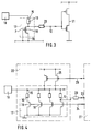
- In Fig. 3 ist die Verwendung der erfindungsgemäßen Schutzstruktur als Eingang eines IC's gezeigt. Die Schutzstruktur 17 zeigt dabei den Transistor 18, zu dem der durch die Widerstandszone 10 gebildete Widerstand in Reihe geschaltet ist. Die mit der Drain-Anschlußzone verbundene Leiterbahn 15 führt zu einem äußeren Anschlußpad 19, über welches das IC mit äußeren Anschlüssen verbunden werden kann. Der Transistor 18 ist in diesem Fall als Diode geschaltet, wobei die Leiterbahn 16 von den Source-Anschlüssen und die Gate-Elektrode 7 mit einem festen Potential, vorzugsweise der Masse verbunden sind. Der Drainbereich des Transistors 18 ist mit seinem Anschluß 12 mit einem Eingangselement 21 des IC's, d.h. des inneren Teils des IC's verbunden. Hier ist das Eingangselement eine CMOS-Inverterstufe.
- In Fig. 4 ist eine weitere Verwendungsmöglichkeit der erfindungsgemäßen Schutzstruktur 17 gezeigt. Die Schutzstruktur 17 wird hier als Teil einer Push-Pull-Ausgangsstufe 22 eines IC's verwendet. Die Schutzstruktur 17 besteht aus mehreren zueinander parallelgeschalteten Transistoren 18, zu deren Drain jeweils ein durch den Widerstandsbereich 10 gebildeter Widerstand in Reihe geschaltet ist. Der Drainanschluß 15 führt zu einem Anschlußpad 19, welches ein Eingangs/Ausgangsanschlußpad ist. Die parallelgeschalteten Transistoren 18 mit ihren Widerstandsbereichen 10 entsprechen einer Schutzstruktur wie sie in Fig. 1 gezeigt ist, mit mehreren parallelgeschalteten Anschlüssen. Der Anschluß 12 der Drainbereiche der Schutzstruktur 17 führt über einen Widerstand 20 zu einem Eingang 23 des inneren Teils des IC's. Die Gate-Elektroden werden von einer aus dem inneren Teil 27 des IC's kommenden Signalleitung 24 angesteuert. Ebenfalls werden die Gate-Elektroden der p-Kanal-Transistoren 25, die den zweiten Zweig der Push-pull-Stufe bilden, von einer Signalleitung 26, die ebenfalls aus dem inneren Teil 27 des IC's kommt, angesteuert. In der Regel ist das W/L-Verhältnis der Transistoren 25 des zweiten Zweiges deutlich größer als das W/L-Verhältnis der Transistoren 18 des ersten Zweiges der Push-Pull-Stufe.
- Im folgenden wird die Funktionsweise der erfindungsgemäßen Transistoranordnung beschrieben. Gelangt ein positiver Spannungspuls beispielsweise über einen äußeren Anschluß des IC's auf die mit diesem Anschluß verbundene Drainanschlußzone, so geht der n-Kanal-MOS-Transistor beim Erreichen der Drain-Source- bzw. der Drain-Substrat-Abbruchspannung in einen bipolaren Betriebszustand über. Dieser Betriebszustand wird auch mit npn-Zustand bezeichnet. Die Leiterbahnen 16 werden typischerweise an Masse angeschlossen. Die n-Wanne 10 bildet einen Serienwiderstand zwischen der Drain-Zone 2 und der Drain-Anschlußzone 4. Ferner bildet sie einen tief in den Substratkörper 1 hineinreichenden pn-Übergang zwischen der Drain-Zone 2 und dem Kanal 11 aus, den Collector-pn-Übergang. Aufgrund des Serienwiderstands dieser n-Wanne werden bei dem Übergang in den pn-Zustand Einschnürungen des an dem pn-Übergang auftretenden Stromes verhindert. Der Transistor kann im Bipolarzustand mehr Leistung als mit herkömmlichen Anordnungen aufnehmen. Durch das Parallelschalten zweier oder mehrerer Transistoren wird der dabei auftretende Strom noch weiter verteilt, so daß die Leistung von beiden Transistoren aufgenommen werden kann, da die Verlustleistung auf eine noch größere Fläche verteilt wird.
Claims (8)
- Schutzstruktur zum Schutz eines Ausgangs oder Eingangs einer integrierten Schaltung (IC) gegen Überspannungen mit einem n-Kanal-MOS-Feldeffekttransistor, dadurch gekennzeichnet, daß die Drain-Zone (2) und die Drainanschlußzone (4) räumlich getrennt voneinander angeordnet sind, und daß im Substrat (1) unterhalb der Drain-Zone (2) und der Drain-Anschlußzone (4) eine n-dotierte Widerstandszone (10) mit einer schwächeren Dotierung als die Dotierung der Drain-Zone (2) und der Drain-Anschlußzone (4) derart ausgebildet ist, daß sie die elektrisch leitende Verbindung zwischen der Drain-Zone (2) und der Drain-Anschlußzone (4) bildet.
- Schutzstruktur nach Anspruch 1, dadurch gekennzeichnet, daß sich die Widerstandszone (10) höchstens bis zu der Gate-/Drain-Kante der Drain-Zone (2) erstreckt.
- Schutzstruktur nach Anspruch 1 oder 2, dadurch gekennzeichnet, daß die Widerstandszone (10) sich unterhalb der gesamten Drain-Anschlußzone (4) erstreckt.
- Schutzstruktur nach einem der vorangehenden Patentansprüche, dadurch gekennzeichnet, daß die Drainzone (2) und die Drainanschlußzone (4) durch eine Isolationsschicht voneinander getrennt sind, welche an der Halbleiteroberfläche liegt.
- Schutzstrukur nach einem der vorangehenden Patentansprüche, dadurch gekennzeichnet, daß die Breite der Widerstandszone (10) mehr als 10 µm, vorzugsweise 100 µm beträgt.
- Schutzstruktur nach einem der vorangehenden Patentansprüche, dadurch gekennzeichnet, daß die Tiefe der Widerstandszone (10) deutlich größer ist als die Tiefe der Drain-Zone (2) bzw. der Drain-Anschlußzone (4), insbesondere um einen Faktor 3 bis 5.
- Schutzstruktur nach einem der vorangehenden Patentansprüche, dadurch gekennzeichnet, daß unterhalb der Source-Zone (3) eine n-Zone mit schwächerer Dotierung als die Dotierung des Source-Zones (3) ausgebildet ist.
- Schutzstruktur nach einem der vorangehenden Patentansprüche, dadurch gekennzeichnet, daß der Drainbereich (2) über einen Anschluß (12) direkt mit einem Eingangselement des IC's, insbesondere einer Gateelektrode, eines Eingangstransistors verbunden ist.
Applications Claiming Priority (2)
| Application Number | Priority Date | Filing Date | Title |
|---|---|---|---|
| DE4423591 | 1994-07-06 | ||
| DE4423591A DE4423591C2 (de) | 1994-07-06 | 1994-07-06 | Schutzstruktur für integrierte Schaltungen |
Publications (3)
| Publication Number | Publication Date |
|---|---|
| EP0691683A2 true EP0691683A2 (de) | 1996-01-10 |
| EP0691683A3 EP0691683A3 (de) | 1996-06-05 |
| EP0691683B1 EP0691683B1 (de) | 2000-05-31 |
Family
ID=6522320
Family Applications (1)
| Application Number | Title | Priority Date | Filing Date |
|---|---|---|---|
| EP95110474A Expired - Lifetime EP0691683B1 (de) | 1994-07-06 | 1995-07-05 | Integrierte Schaltung mit Schutzstruktur |
Country Status (4)
| Country | Link |
|---|---|
| US (1) | US5565698A (de) |
| EP (1) | EP0691683B1 (de) |
| JP (2) | JPH0855984A (de) |
| DE (2) | DE4423591C2 (de) |
Cited By (3)
| Publication number | Priority date | Publication date | Assignee | Title |
|---|---|---|---|---|
| EP0807977A3 (de) * | 1996-05-17 | 2000-03-15 | Texas Instruments Incorporated | Halbleiteranordnung mit einer Schutzvorrichtung |
| WO2002059970A3 (de) * | 2001-01-25 | 2003-08-07 | Infineon Technologies Ag | Mos-transistor |
| EP1363329A3 (de) * | 2002-05-18 | 2008-10-22 | Micronas GmbH | Schutzstruktur gegen elektrostatische Entladungen |
Families Citing this family (12)
| Publication number | Priority date | Publication date | Assignee | Title |
|---|---|---|---|---|
| US5654860A (en) * | 1995-08-16 | 1997-08-05 | Micron Technology, Inc. | Well resistor for ESD protection of CMOS circuits |
| AU1123597A (en) * | 1995-11-30 | 1997-06-19 | Micron Technology, Inc. | Structure for esd protection in semiconductor chips |
| US6507074B2 (en) | 1995-11-30 | 2003-01-14 | Micron Technology, Inc. | Structure for ESD protection in semiconductor chips |
| US5663678A (en) * | 1996-02-02 | 1997-09-02 | Vanguard International Semiconductor Corporation | ESD protection device |
| US5808343A (en) * | 1996-09-20 | 1998-09-15 | Integrated Device Technology, Inc. | Input structure for digital integrated circuits |
| KR100482362B1 (ko) * | 1997-10-14 | 2005-08-01 | 삼성전자주식회사 | 정전기보호용반도체장치및그제조방법 |
| US6100125A (en) * | 1998-09-25 | 2000-08-08 | Fairchild Semiconductor Corp. | LDD structure for ESD protection and method of fabrication |
| ATE222415T1 (de) * | 1998-09-25 | 2002-08-15 | Infineon Technologies Ag | Schutzschaltung auf einer integrierten schaltung |
| JP3430080B2 (ja) | 1999-10-08 | 2003-07-28 | Necエレクトロニクス株式会社 | 半導体装置及びその製造方法 |
| US8299531B1 (en) * | 2001-12-27 | 2012-10-30 | National Semiconductor Corporation | CMOS ESD clamp with input and separate output voltage terminal for ESD protection |
| EP1403909A1 (de) * | 2002-09-30 | 2004-03-31 | STMicroelectronics S.r.l. | Verfahren zur Herstellung integrierter Widerstandselemente mit Silizidationsschutz |
| JP4993941B2 (ja) * | 2006-04-27 | 2012-08-08 | パナソニック株式会社 | 半導体集積回路及びこれを備えたシステムlsi |
Family Cites Families (11)
| Publication number | Priority date | Publication date | Assignee | Title |
|---|---|---|---|---|
| US4246592A (en) * | 1979-01-02 | 1981-01-20 | Texas Instruments Incorporated | High density static memory cell |
| JPH0691196B2 (ja) * | 1984-07-25 | 1994-11-14 | 株式会社日立製作所 | 半導体装置 |
| FR2598852B1 (fr) * | 1986-05-16 | 1988-10-21 | Eurotechnique Sa | Dispositif de protection d'entree pour circuits integres en technologie cmos. |
| US4987465A (en) * | 1987-01-29 | 1991-01-22 | Advanced Micro Devices, Inc. | Electro-static discharge protection device for CMOS integrated circuit inputs |
| US4902640A (en) * | 1987-04-17 | 1990-02-20 | Tektronix, Inc. | High speed double polycide bipolar/CMOS integrated circuit process |
| US5270565A (en) * | 1989-05-12 | 1993-12-14 | Western Digital Corporation | Electro-static discharge protection circuit with bimodal resistance characteristics |
| JPH03272180A (ja) * | 1990-03-22 | 1991-12-03 | Toshiba Corp | 半導体集積回路 |
| US5272097A (en) * | 1992-04-07 | 1993-12-21 | Philip Shiota | Method for fabricating diodes for electrostatic discharge protection and voltage references |
| US5371395A (en) * | 1992-05-06 | 1994-12-06 | Xerox Corporation | High voltage input pad protection circuitry |
| US5838033A (en) * | 1993-09-08 | 1998-11-17 | Lucent Technologies Inc. | Integrated circuit with gate conductor defined resistor |
| US5440162A (en) * | 1994-07-26 | 1995-08-08 | Rockwell International Corporation | ESD protection for submicron CMOS circuits |
-
1994
- 1994-07-06 DE DE4423591A patent/DE4423591C2/de not_active Expired - Fee Related
-
1995
- 1995-07-05 DE DE59508413T patent/DE59508413D1/de not_active Expired - Fee Related
- 1995-07-05 EP EP95110474A patent/EP0691683B1/de not_active Expired - Lifetime
- 1995-07-06 US US08/498,822 patent/US5565698A/en not_active Expired - Fee Related
- 1995-07-06 JP JP7171051A patent/JPH0855984A/ja not_active Withdrawn
-
2007
- 2007-04-04 JP JP2007098617A patent/JP2007235151A/ja not_active Withdrawn
Non-Patent Citations (1)
| Title |
|---|
| CHARVAKA DUVVURY, ROBERT ROUNTREE: "EOS/ESD Symposium Proceedings 1991", 1991, pages: 88 |
Cited By (4)
| Publication number | Priority date | Publication date | Assignee | Title |
|---|---|---|---|---|
| EP0807977A3 (de) * | 1996-05-17 | 2000-03-15 | Texas Instruments Incorporated | Halbleiteranordnung mit einer Schutzvorrichtung |
| WO2002059970A3 (de) * | 2001-01-25 | 2003-08-07 | Infineon Technologies Ag | Mos-transistor |
| EP1363329A3 (de) * | 2002-05-18 | 2008-10-22 | Micronas GmbH | Schutzstruktur gegen elektrostatische Entladungen |
| DE10222306B4 (de) * | 2002-05-18 | 2010-11-25 | Micronas Gmbh | Schutzstruktur gegen elektrostatische Entladungen |
Also Published As
| Publication number | Publication date |
|---|---|
| JP2007235151A (ja) | 2007-09-13 |
| JPH0855984A (ja) | 1996-02-27 |
| DE4423591C2 (de) | 1996-08-29 |
| EP0691683B1 (de) | 2000-05-31 |
| US5565698A (en) | 1996-10-15 |
| DE59508413D1 (de) | 2000-07-06 |
| DE4423591A1 (de) | 1996-01-11 |
| EP0691683A3 (de) | 1996-06-05 |
Similar Documents
| Publication | Publication Date | Title |
|---|---|---|
| DE19518549C2 (de) | MOS-Transistor getriggerte Schutzschaltung gegen elektrostatische Überspannungen von CMOS-Schaltungen | |
| DE102016106309B4 (de) | Hochgeschwindigkeits-Schnittstellenschutzvorrichtung | |
| DE19533958C2 (de) | Schutzschaltung gegen elektrostatische Entladungen enthaltend eine Kondensatorschaltung | |
| DE69527146T2 (de) | Integriertes MOS-Bauelement mit einer Gateschutzdiode | |
| DE69938523T2 (de) | ESD-Schutzthyristor mit Triggerdiode | |
| DE69319021T2 (de) | Eingangsschutzschaltung mit einer hohen Spannungsfestigkeit | |
| DE4423030C2 (de) | Schutzschaltung gegen elektrostatische Entladung für eine Halbleitereinrichtung | |
| DE69232257T2 (de) | Durch Verarmung kontrollierte Isolationsstufe | |
| EP0691683B1 (de) | Integrierte Schaltung mit Schutzstruktur | |
| DE102008036834B4 (de) | Diodenbasiertes ESE-Konzept für Demos-Schutz | |
| DE9209990U1 (de) | Integrierte Schaltung mit MOS-Kondensator für verbesserten elektrostatischen Entladungsschutz | |
| DE19654163B4 (de) | Schutzvorrichtung für eine Halbleiterschaltung | |
| DE2544438A1 (de) | Integrierte ueberspannungs-schutzschaltung | |
| DE10239230A1 (de) | Hochfrequenz-Halbleitervorrichtung | |
| DE102012014860A1 (de) | ESD-Schutz | |
| DE10216015A1 (de) | Überspannungsschutzschaltung | |
| DE3784793T2 (de) | Integrierte schaltung mit verbesserter schutzvorrichtung. | |
| DE68916192T2 (de) | Ausgangspuffer einer integrierten Schaltung mit einem verbesserten ESD-Schutz. | |
| DE19712834B4 (de) | Schutzschaltung und Schaltung für eine Halbleiter-Auf-Isolator-Vorrichtung | |
| DE69031562T2 (de) | Durch eine niedrige spannung auslösbare rückstellungsanordnung | |
| DE19504541A1 (de) | Eingangsschaltung zum Schützen einer monolithischen integrierten Schaltung | |
| DE102005019305B4 (de) | ESD-Schutzstruktur mit Diodenreihenschaltung und Halbleiterschaltung mit derselben | |
| DE102019102695B4 (de) | Unterdrückung von parasitären Entladungspfaden in einer elektrischen Schaltung | |
| EP1127377B1 (de) | Esd-schutztransistor | |
| DE102008047850B4 (de) | Halbleiterkörper mit einer Schutzstruktur und Verfahren zum Herstellen derselben |
Legal Events
| Date | Code | Title | Description |
|---|---|---|---|
| PUAI | Public reference made under article 153(3) epc to a published international application that has entered the european phase |
Free format text: ORIGINAL CODE: 0009012 |
|
| AK | Designated contracting states |
Kind code of ref document: A2 Designated state(s): CH DE FR GB IT LI NL |
|
| PUAL | Search report despatched |
Free format text: ORIGINAL CODE: 0009013 |
|
| AK | Designated contracting states |
Kind code of ref document: A3 Designated state(s): CH DE FR GB IT LI NL |
|
| 17P | Request for examination filed |
Effective date: 19961205 |
|
| RAP1 | Party data changed (applicant data changed or rights of an application transferred) |
Owner name: MICRONAS INTERMETALL GMBH |
|
| 17Q | First examination report despatched |
Effective date: 19981102 |
|
| GRAG | Despatch of communication of intention to grant |
Free format text: ORIGINAL CODE: EPIDOS AGRA |
|
| RTI1 | Title (correction) |
Free format text: INTEGRATED CIRCUIT WITH PROTECTION STRUCTURE |
|
| GRAG | Despatch of communication of intention to grant |
Free format text: ORIGINAL CODE: EPIDOS AGRA |
|
| GRAH | Despatch of communication of intention to grant a patent |
Free format text: ORIGINAL CODE: EPIDOS IGRA |
|
| GRAH | Despatch of communication of intention to grant a patent |
Free format text: ORIGINAL CODE: EPIDOS IGRA |
|
| GRAA | (expected) grant |
Free format text: ORIGINAL CODE: 0009210 |
|
| AK | Designated contracting states |
Kind code of ref document: B1 Designated state(s): CH DE FR GB IT LI NL |
|
| REG | Reference to a national code |
Ref country code: CH Ref legal event code: EP |
|
| REG | Reference to a national code |
Ref country code: CH Ref legal event code: NV Representative=s name: WILLIAM BLANC & CIE CONSEILS EN PROPRIETE INDUSTRI |
|
| GBT | Gb: translation of ep patent filed (gb section 77(6)(a)/1977) |
Effective date: 20000612 |
|
| REF | Corresponds to: |
Ref document number: 59508413 Country of ref document: DE Date of ref document: 20000706 |
|
| ITF | It: translation for a ep patent filed | ||
| ET | Fr: translation filed | ||
| RAP2 | Party data changed (patent owner data changed or rights of a patent transferred) |
Owner name: MICRONAS GMBH |
|
| REG | Reference to a national code |
Ref country code: CH Ref legal event code: PFA Free format text: MICRONAS INTERMETALL GMBH TRANSFER- MICRONAS GMBH |
|
| NLT2 | Nl: modifications (of names), taken from the european patent patent bulletin |
Owner name: MICRONAS GMBH |
|
| PLBE | No opposition filed within time limit |
Free format text: ORIGINAL CODE: 0009261 |
|
| STAA | Information on the status of an ep patent application or granted ep patent |
Free format text: STATUS: NO OPPOSITION FILED WITHIN TIME LIMIT |
|
| 26N | No opposition filed | ||
| REG | Reference to a national code |
Ref country code: GB Ref legal event code: IF02 |
|
| PGFP | Annual fee paid to national office [announced via postgrant information from national office to epo] |
Ref country code: DE Payment date: 20070831 Year of fee payment: 13 |
|
| PGFP | Annual fee paid to national office [announced via postgrant information from national office to epo] |
Ref country code: CH Payment date: 20070730 Year of fee payment: 13 |
|
| PGFP | Annual fee paid to national office [announced via postgrant information from national office to epo] |
Ref country code: GB Payment date: 20070727 Year of fee payment: 13 |
|
| PGFP | Annual fee paid to national office [announced via postgrant information from national office to epo] |
Ref country code: NL Payment date: 20070724 Year of fee payment: 13 Ref country code: IT Payment date: 20070727 Year of fee payment: 13 |
|
| PGFP | Annual fee paid to national office [announced via postgrant information from national office to epo] |
Ref country code: FR Payment date: 20070717 Year of fee payment: 13 |
|
| REG | Reference to a national code |
Ref country code: CH Ref legal event code: PL |
|
| GBPC | Gb: european patent ceased through non-payment of renewal fee |
Effective date: 20080705 |
|
| NLV4 | Nl: lapsed or anulled due to non-payment of the annual fee |
Effective date: 20090201 |
|
| PG25 | Lapsed in a contracting state [announced via postgrant information from national office to epo] |
Ref country code: DE Free format text: LAPSE BECAUSE OF NON-PAYMENT OF DUE FEES Effective date: 20090203 |
|
| REG | Reference to a national code |
Ref country code: FR Ref legal event code: ST Effective date: 20090331 |
|
| PG25 | Lapsed in a contracting state [announced via postgrant information from national office to epo] |
Ref country code: NL Free format text: LAPSE BECAUSE OF NON-PAYMENT OF DUE FEES Effective date: 20090201 |
|
| PG25 | Lapsed in a contracting state [announced via postgrant information from national office to epo] |
Ref country code: LI Free format text: LAPSE BECAUSE OF NON-PAYMENT OF DUE FEES Effective date: 20080731 Ref country code: GB Free format text: LAPSE BECAUSE OF NON-PAYMENT OF DUE FEES Effective date: 20080705 Ref country code: CH Free format text: LAPSE BECAUSE OF NON-PAYMENT OF DUE FEES Effective date: 20080731 |
|
| PG25 | Lapsed in a contracting state [announced via postgrant information from national office to epo] |
Ref country code: IT Free format text: LAPSE BECAUSE OF NON-PAYMENT OF DUE FEES Effective date: 20080705 Ref country code: FR Free format text: LAPSE BECAUSE OF NON-PAYMENT OF DUE FEES Effective date: 20080731 |