EP0691742A2 - Récepteur optique avec un préamplificateur à impédance élevée - Google Patents
Récepteur optique avec un préamplificateur à impédance élevée Download PDFInfo
- Publication number
- EP0691742A2 EP0691742A2 EP95304548A EP95304548A EP0691742A2 EP 0691742 A2 EP0691742 A2 EP 0691742A2 EP 95304548 A EP95304548 A EP 95304548A EP 95304548 A EP95304548 A EP 95304548A EP 0691742 A2 EP0691742 A2 EP 0691742A2
- Authority
- EP
- European Patent Office
- Prior art keywords
- diode
- photodiode
- circuit
- load
- voltage
- Prior art date
- Legal status (The legal status is an assumption and is not a legal conclusion. Google has not performed a legal analysis and makes no representation as to the accuracy of the status listed.)
- Withdrawn
Links
Images

Classifications
-
- H—ELECTRICITY
- H03—ELECTRONIC CIRCUITRY
- H03K—PULSE TECHNIQUE
- H03K17/00—Electronic switching or gating, i.e. not by contact-making and –breaking
- H03K17/51—Electronic switching or gating, i.e. not by contact-making and –breaking characterised by the components used
- H03K17/78—Electronic switching or gating, i.e. not by contact-making and –breaking characterised by the components used using opto-electronic devices, i.e. light-emitting and photoelectric devices electrically- or optically-coupled
- H03K17/785—Electronic switching or gating, i.e. not by contact-making and –breaking characterised by the components used using opto-electronic devices, i.e. light-emitting and photoelectric devices electrically- or optically-coupled controlling field-effect transistor switches
Definitions
- the present invention relates to optical receivers employing high impedance preamplifiers, and in particular, integrated circuits employing such receivers.
- Integrated circuits such as memory chips and microprocessors, may communicate data by transmitting and receiving optical signals.
- Integrated circuits presently effect the transmission and reception of optical signals using Self-Electrooptic Effect Devices (SEEDs). See, Woodward, et al, "Operating characteristics of GaAs/AlGaAs FET-SEED Smart Pixels," 1992 IEDM Tech. Digest p. 655 (IEEE 1992), which is incorporated herein by reference.
- SEEDs Self-Electrooptic Effect Devices
- An integrated circuit employing SEED technology contains arrays of optical receivers and optical modulators which receive and transmit data respectively.
- Optical receiver circuits such as those employed in SEED-based communication systems typically include a preamplifier stage comprising a light detecting device and an amplification device.
- the preamplifier stage receives light wave or optical signals and provides at its output an electrical signal that is representative of the received optical signal.
- a number of constraints apply to SEED optical receivers that do not apply in a typical photo-receiver. One constraint is the requirement of a small footprint. Another requirement is that the SEED optical receiver must produce output signals compatible with processing by electronic logic circuitry.
- transimpedance preamplifier stage Two classes of preamplifier stages have gained favor with circuit designers, the transimpedance preamplifier stage and the high impedance preamplifier stage.
- the primary difference between the amplifiers is that transimpedance amplifiers are closed loop devices while high impedance amplifiers are open loop devices.
- Each class of preamplifiers has its advantages and disadvantages. High impedance preamplifiers, however, combine high sensitivity with a minimal component count, which helps satisfy the constraints discussed above.
- integrated circuits employing SEED technology may include an array of optical receivers, each including a high impedance preamplifier stage. Although the use of high impedance preamplifiers reduces the receiver footprint, still further reduction is advantageous.
- FET field effect transistor
- the present invention provides a novel single beam optical receiver including a high impedance amplifier.
- the receiver consists of an optical detecting device connected to both the gate of an FET device and a load diode providing a load impedance.
- the FET device is connected to a biasing voltage through a biasing impedance, forming a high gain inverter.
- the use of a diode to provide a load impedance allows for a smaller and easier to manufacture receiver circuit than would be possible using either a load resistor or a load FET.
- a digital integrated circuit employing SEED technology incorporates a plurality of such diode-loaded optical receivers to facilitate optical communications between integrated circuits with minimal consumption of space.
- FIG. 1 illustrates an exemplary prior art high impedance optical receiver 100.
- the receiver 100 receives a light signal at its input, a photodiode 105, and produces an amplified electrical signal representative of the incoming optical signal at an output 108.
- the cathode of the photodiode 105 is connected to a positive bias voltage VBIAS+ while its anode is connected to both the gate of an FET 110 and a load resistor 115.
- the load resistor 115 is further connected to a negative bias voltage VBIAS-.
- the FET 110 is coupled to the output 108 and is further connected to VBIAS+ through a bias resistor 125, forming a known type of high impedance inverter.
- the photodiode 105 When a strong light signal strikes the photodiode 105, the photodiode 105 conducts current in reverse mode, or in other words, from cathode to anode. Thus, current flows from VBIAS+ to VBIAS- through the load resistor 115, thereby raising the gate voltage of the FET 110 in excess of the inverter threshold voltage.
- the inverter threshold voltage is a voltage above which the inverter produces a low output voltage and below which the inverter produces a high input voltage.
- the photodiode 105 When the strong light signal is removed or replaced by a weak light signal, the photodiode 105 ceases to conduct current, and the lack of current will decrease the voltage appearing across the load resistor and at the gate of the FET 110. The voltage at the gate of the FET 110 falls below the threshold voltage of the inverter. As a result, the inverter formed by the FET 110 and the resistor 125 will produce a high output voltage.
- the receiver 100 is only useful for a limited range of input currents. Because the resistor 115 has a linear relationship between current and voltage, the voltage change induced by increasingly large input current variations increases without bounds. Such large voltage excursions may saturate or otherwise adversely affect the operation of the FET 110, thereby limiting the useful range of input currents that can be accommodated.
- a second photodiode may be implemented to provide the required discharge path. See Woodward, et al., "Operating Characteristics of GaAs/AlGaAs FET-SEED Smart Pixels," cited above. In such an implementation however, a second light beam is required to activate the discharge path when the original strong light signal is removed.
- FIG. 2 illustrates a circuit including a novel high impedance single beam optical receiver 200 comprising a photodiode 205, an FET 210 having a gate 211, a drain 212 and a source 213, a load diode 215, and a bias FET 225.
- the photodiode 205 which may suitably be a GaAs multiple quantum well p-i-n, a p-i-n, metal semiconductor, Schottky or an avalanche photodiode, comprises an anode and a cathode.
- the cathode is connected to a first bias voltage VBIAS+ and the anode is connected to both the gate 211 of the FET 210 and the anode of the load diode 215.
- the load diode 215 may suitably be a GaAs p-n junction diode, a Schottky diode, a p-i-n junction diode, or a silicon-based diode.
- the photodiode 205 is reverse biased with respect to the load diode 215.
- the cathode of load diode 215 is connected to a balancing voltage, VBAL-.
- the voltages VB IAS+ and VBAL- may suitably be +10 Vdc and -1 Vdc, respectively. Such voltage levels are given by way of example, other suitable levels may be employed. The relationship between the operation of the circuit and VBIAS+ and VBAL- is explained further below.
- the drain 212 of the FET 210 is connected to a second bias voltage, which may suitably be the same as the first bias voltage, VBIAS+, through the bias FET 225.
- the FET 210 and the bias FET 225 as configured, comprise a known form of a high gain inverter that provides preamplification and operates in essentially the same manner as the inverter discussed above in connection with FIG. 1.
- the high gain inverter formed by the FETs 210 and 225 produces at its output, which is the drain 212 of the FET 210, a high logic voltage level or a low logic voltage level, depending upon the input voltage at the gate 211.
- the FETs 210 and 225 may be GaAs doped channel heterojunction FETs, doped channel HFETs, GaAs MESFETs, or silicon based FETs.
- the source 213 of the FET 210 is connected to ground.
- the photodiode 205 is a GaAs multiple quantum well (mqw) p-i-n modulator
- the load diode 215 is a GaAs Schottky diode
- the FETs 205 and 225 are GaAs doped-channel heterojunction FETs.
- the inverter formed by the FETs 205 and 225 exhibits a threshold voltage of approximately -0.3 Vdc in this embodiment.
- the receiver 200 receives digital light signals, the digital light signals having a first level of intensity representative of one binary value and a second intensity level representative of the other binary value.
- a signal of the first intensity level will be referred to as a strong light signal and a signal of the second intensity level will be referred to as either a weak light signal or the lack of a strong light signal.
- the receiver 200 converts the digital light signals into digital electrical signals in the manner discussed below.
- the photodiode 205 When a strong light signal strikes the photodiode 205, the photodiode 205 conducts current at a first current level.
- the first current level is imposed upon the load diode 215, forward biasing the load diode 215 and causing the load diode 215 to exhibit a first voltage drop V d1 in accordance with its voltage-current or v-i characteristic.
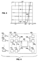
- FIG. 3 A typical v-i characteristic for a forward-biased diode is illustrated in FIG. 3.
- the curve 310 is flat and very little current is conducted.
- the current curve 320 increases rapidly as a function of bias voltage.
- the load diode 215 should be chosen such that the current from the photodiode 205 under a strong light signal causes V d1 to exceed the threshold 315, for reasons that will be explained further below.
- a 10 ⁇ W light signal may be used to provide a strong light signal, which in turn causes the photodiode 215 to conduct current at approximately 5 ⁇ A.
- the load diode 215 in this embodiment exhibits a voltage drop of approximately 0.72 vdc at 5 ⁇ A of current.
- VBAL- should be chosen such that VBAL-, when added to V d1 , produces a voltage at the gate 211 that exceeds the inverter threshold voltage.
- VBAL- is suitably -1 Vdc.
- the photodiode 205 produces a current at a second level that is lower than the first current level.
- the second level of photodiode current may suitably comprise essentially no current.
- the inherent capacitance of the gate 211 maintains the first voltage drop level, V d1 , across the load diode 215. This charge on the gate 211 subsequently discharges through the load diode 215. As the gate 211 discharges, the voltage drop across the diode 215 decreases, and the discharge current decreases. In other words, the voltage drop of the load diode 215 moves from right-to-left on the graph in FIG. 3.
- the gate 211 continues to discharge at least until the voltage at the gate falls sufficiently below the inverter threshold to change the inventor output to the high logic level.
- the voltage drop exhibited by the load diode 215 is defined as V d2 , where V d2 comprises a second load diode voltage drop that is lower than V d1 .
- the voltage at the drain 212 of the FET 210 then rises to a high logic voltage level. It should be noted that because V d1 was chosen on a point on the portion 320 of the curve in FIG. 3, relatively large levels of discharge current flow through the diode 215, allowing the gate to discharge to below the inverter threshold voltage fairly rapidly, which is essential for high speed operation.
- VBAL- must be adjusted so that V d1 and V d2 cause the voltage at the gate 211 to fall on either side of the inverter threshold voltage.
- the load diode 215 should preferably exhibit at least a 200 mV difference between V d1 and V d2 , to insure complete switching of the inverter during high frequency operation of on the order of 200 Mbit/s. This requirement is due to the fact that an inverter does not switch perfectly at its gate threshold voltage, but over a range, which in the case of the inverter used in embodiment A is 30 mv. Diodes having suitable v-i characteristics may be readily selected by those of ordinary skill in the art.
- the receiver 200 produces an electrical binary signal version of the input digital light signal, and, moreover, offers spatial advantages and manufacturing advantages over the receiver 100 illustrated in FIG. 1.
- the circuit 200 consumes less chip surface space.
- diodes are less costly to incorporate into a integrated circuit than resistors.
- the known alternative of replacing the load resistor with an FET, while constituting an improvement nevertheless occupies more surface area than the load diode.
- the diode has ideally an exponential relationship between current and voltage, an improved dynamic range of input currents may be accommodated. Large input currents do not produce excessively large voltage excursions at the input to the FET 210 as they would using a load resistor because the load diode 215 tends to saturate.
- a diode is not typically used as a resistor substitute, such as, for example, an FET with its gate tied to its source, primarily because the diode response is extremely nonlinear. This nonlinearity introduces substantial distortion that would be unacceptable in many circuits in which an optical receiver is used. It has been found, however, that for an optical receiver used for digital signal transmission between integrated circuits, the load need not behave predominately as a resistor.
- the flexible load requirement is due in part to the nature of digital communications wherein the optical signal only has two states, high (1) or low (0). As a result, the signal distortion caused by the nonlinear diode response is tolerable.
- FIG. 4 illustrates an integrated circuit 400 which is operable to accomplish opto-electrical interconnection with other integrated circuits using FET-SEED technology.
- An integrated circuit as described herein means a circuit having all circuit elements built into a single semiconductor substrate.
- the integrate circuit 400 may be either monolithically integrated or hybrid. Particular details regarding FET-SEED communication between integrated circuits may be found for example, in Woodward, et al., "GaAs/AlGaAs FET-SEED Receiver/Transmitters," OSA Proc. on Photonics in Switching p. 89 (Optical Society of America 1993), which is incorporated herein by reference; and Woodward, et al., "Operating Characteristics of GaAs/AlGaAs FET-SEED Smart Pixels," cited above.
- the integrated circuit 400 is situated in a location within a circuit arrangement, not shown, to receive directed optical input signals from a substantial plurality of sources 4051 through 405 n .
- the optical signal sources 4051 through 405 n may suitably comprise FET-SEED modulators located on one or more other integrated circuits, not shown.
- the integrated circuit 400 comprises a monolithic GaAs chip having a substantial plurality of optical detectors 4101 through 410 n , each of which is connected to one of a substantial plurality of signal conditioning devices 4151 through 415 n .
- Each of the detectors 4101 through 410 n comprises the optical receiver circuit 200 discussed above in connection with FIG. 2.
- the signal conditioning devices 4151 through 415 n comprise any suitable circuit elements capable of converting input binary signals to signal levels appropriate for the particular logic family used. Circuitry capable of producing appropriate BJT levels, FET levels or levels compatible with any other standard logic family is well known to those of ordinary skill in the art.
- the signal conditioning devices 4151 through 415 n are in turn coupled by lines 4201 through 420 n to a block of digital processing circuitry 425.
- the digital processing circuitry 425 may comprise a series of logic gates, a gate array, or one or more microprocessors.
- the precise number of the substantial plurality of optical detectors 4101 through 410 n depends on the digital processing circuitry involved.
- the advantages of the present invention are substantial in circuits having over 100 parallel inputs.
- digital processing circuitry such as, for example, a large scale random access memory, an advanced microprocessor or parallel processor often requires 1000 parallel inputs or more.
- the size advantages of the present invention are further amplified with respect to such devices.
- Various output lines 4301 through 430 m of the digital processing circuitry 425 are coupled to line driver circuits 4351 through 435 m .
- Each of the line driver circuits 4351 through 435 m may suitably comprise a SEED-type modulator for producing optical output signals. See, for example, "GaAs/AlGaAs FET-SEED Receiver/Transmitters", cited above.
- a plurality of digital optical signals from a plurality of optical signal sources 4051 through 405 n strike a plurality of detector circuits 4101 through 420 n .
- each digital optical signal OPT X is directed to strike a particular detector circuit 410 x .
- Techniques for generating and directing optical signals between integrated circuits are well known. F.B. McCormick et al., "Six Stage Digital Free Space Optical Switching Network Using Symmetric Self-Electrooptic Effect Devices," Applied Optics , Vol. 32, p. 5153 (September 10, 1993).
- Each detector circuit 410 x then produces at its output an electrical binary signal EL X in some form.
- electrical binary signal it is meant that one voltage level represents a “1” value and another voltage level represents a “0” value.
- the signal conditioning circuits 4151 through 415 n adjust these "1" and “0" voltage levels so that they conform with the levels required by the logic family employed in the digital circuitry 425.
- the optical detectors 4101 through 410 n produce binary signal levels which are already compatible with the digital circuitry 425. In such cases, the signal conditioning circuits 4151 through 415 n are not required.
- each conditioned signal EL X is provided to the digital processing circuitry 425 through an input line 420 x .
- each detector circuit 410 x is physically located in close proximity to the portion of the digital processing circuitry 425 that processes the input from the signal source 405 x . This placement of the detector circuits 4101 through 410 n minimizes the physical length of the input lines 4201 through 420 n which in turn conserves substrate area.
- the digital circuitry 425 processes the incoming data and provides a plurality of output signals on output lines 4301 through 430 m .
- the output signals are provided to line drivers 4351 through 435 m .
- the line drivers 4351 through 435 m then prepare and transmit the outgoing signals by known techniques.
- the positions of the photodiode 205 and the load diode 215 of the circuit illustrated in FIG. 2 may be interchanged to form a non-inverting receiver.
- the appropriate bias voltages required to implement such an embodiment would be apparent to one of ordinary skill in the art.
- the load resistor serves to provide a load impedance for voltage levels at which the load diode 215 conducts very little current. While the addition of the load resistor somewhat improves the range of inverter threshold voltage levels which may be accommodated, the spatial advantages of the present invention are lost.
- the bias FET 225 provides a biasing impedance for the FET 210 in FIG. 2 above, a resistor or other suitable biasing impedance may be used, although at some spatial cost.
- the load diode 215 is shown as a discrete element in FIG. 2, an inherent diode formed by the gate-source junction of some FETs, which are well known to those of ordinary skill in the art, may instead be employed as the load diode 215, if appropriate biasing levels are employed.
- the integrated circuit 400 may be formed from a material other than GaAs, such as silicon.
Landscapes
- Amplifiers (AREA)
- Light Receiving Elements (AREA)
- Solid State Image Pick-Up Elements (AREA)
- Optical Communication System (AREA)
Applications Claiming Priority (2)
| Application Number | Priority Date | Filing Date | Title |
|---|---|---|---|
| US08/270,952 US5581077A (en) | 1994-07-05 | 1994-07-05 | Optical receiver with a high impedance preamplifier |
| US270952 | 1999-03-16 |
Publications (2)
| Publication Number | Publication Date |
|---|---|
| EP0691742A2 true EP0691742A2 (fr) | 1996-01-10 |
| EP0691742A3 EP0691742A3 (fr) | 1997-09-03 |
Family
ID=23033549
Family Applications (1)
| Application Number | Title | Priority Date | Filing Date |
|---|---|---|---|
| EP95304548A Withdrawn EP0691742A3 (fr) | 1994-07-05 | 1995-06-28 | Récepteur optique avec un préamplificateur à impédance élevée |
Country Status (4)
| Country | Link |
|---|---|
| US (1) | US5581077A (fr) |
| EP (1) | EP0691742A3 (fr) |
| JP (1) | JPH0846445A (fr) |
| CA (1) | CA2149928C (fr) |
Cited By (5)
| Publication number | Priority date | Publication date | Assignee | Title |
|---|---|---|---|---|
| WO1999033168A1 (fr) * | 1997-12-22 | 1999-07-01 | Telefonaktiebolaget Lm Ericsson | Polarisation de transistor basse tension |
| WO2005008196A3 (fr) * | 2003-07-22 | 2005-05-12 | Koninkl Philips Electronics Nv | Procede et dispositif de mesure de la temperature de couleur |
| WO2013083889A1 (fr) * | 2011-12-08 | 2013-06-13 | Societe Francaise De Detecteurs Infrarouges - Sofradir | Dispositif de détection de rayonnement électromagnétique impulsionnel |
| US8725005B2 (en) | 2009-02-23 | 2014-05-13 | Hewlett-Packard Development Company, L.P. | Dynamic impedance photodetector receiver circuit |
| US11108397B2 (en) * | 2018-03-13 | 2021-08-31 | Kay C. Robinson, JR. | Fiber-optic connected logic (FOCL) |
Families Citing this family (22)
| Publication number | Priority date | Publication date | Assignee | Title |
|---|---|---|---|---|
| US5747791A (en) * | 1996-04-25 | 1998-05-05 | Coroy; Trenton G. | Method and devices for wavelength and power demodulation based on the use of a quantum well electroabsorption filtering detector |
| US5869857A (en) * | 1997-04-07 | 1999-02-09 | Chen; Pao-Jung | CMOS photodetectors with wide range operating region |
| US6043525A (en) * | 1997-04-07 | 2000-03-28 | Chen; Pao-Jung | High speed CMOS photodetectors with wide range operating region |
| US6201270B1 (en) * | 1997-04-07 | 2001-03-13 | Pao-Jung Chen | High speed CMOS photodetectors with wide range operating region and fixed pattern noise reduction |
| US5892220A (en) * | 1997-08-05 | 1999-04-06 | Lucent Technologies Inc. | Linearized feedback element for two-beam smart pixel receivers |
| US5920065A (en) * | 1997-11-14 | 1999-07-06 | The United States Of America As Represented By The Secretary Of The Navy | Optically activated back-to-back PIN diode switch having exposed intrinsic region |
| FR2777080B1 (fr) * | 1998-04-07 | 2002-01-18 | Alain Maurice Ange Magagnini | Dispositif electronique de detection a tres faible consommation pour exploiter de maniere continue un capteur a tres haute impedance interne: pyro-electrique, piezo-electrique, micro electrostatique |
| US6198580B1 (en) | 1998-08-17 | 2001-03-06 | Newport Corporation | Gimballed optical mount |
| US6516130B1 (en) | 1998-12-30 | 2003-02-04 | Newport Corporation | Clip that aligns a fiber optic cable with a laser diode within a fiber optic module |
| US6996506B2 (en) | 1999-02-23 | 2006-02-07 | Newport Corporation | Process and device for displacing a moveable unit on a base |
| FR2790115B1 (fr) | 1999-02-23 | 2001-05-04 | Micro Controle | Procede et dispositif pour deplacer un mobile sur une base montee elastiquement par rapport au sol |
| US6511035B1 (en) | 1999-08-03 | 2003-01-28 | Newport Corporation | Active vibration isolation systems with nonlinear compensation to account for actuator saturation |
| US6649898B1 (en) * | 2000-06-30 | 2003-11-18 | Intel Corporation | Method and apparatus for optically enabling a circuit component in a large scale integrated circuit |
| US6655840B2 (en) | 2001-02-13 | 2003-12-02 | Newport Corporation | Stiff cross roller bearing configuration |
| US6601524B2 (en) | 2001-03-28 | 2003-08-05 | Newport Corporation | Translation table with a spring biased dovetail bearing |
| US6791058B2 (en) | 2001-04-25 | 2004-09-14 | Newport Corporation | Automatic laser weld machine for assembling photonic components |
| US6568666B2 (en) | 2001-06-13 | 2003-05-27 | Newport Corporation | Method for providing high vertical damping to pneumatic isolators during large amplitude disturbances of isolated payload |
| US6619611B2 (en) | 2001-07-02 | 2003-09-16 | Newport Corporation | Pneumatic vibration isolator utilizing an elastomeric element for isolation and attenuation of horizontal vibration |
| US6966535B2 (en) | 2002-05-07 | 2005-11-22 | Newport Corporation | Snubber for pneumatically isolated platforms |
| US7603042B2 (en) * | 2002-06-04 | 2009-10-13 | Eiselt Michael H | Apparatus and method for optimum decision threshold setting |
| US7320455B2 (en) | 2003-10-24 | 2008-01-22 | Newport Corporation | Instrumented platform for vibration-sensitive equipment |
| US8231098B2 (en) | 2004-12-07 | 2012-07-31 | Newport Corporation | Methods and devices for active vibration damping of an optical structure |
Family Cites Families (8)
| Publication number | Priority date | Publication date | Assignee | Title |
|---|---|---|---|---|
| US4447746A (en) * | 1981-12-31 | 1984-05-08 | International Business Machines Corporation | Digital photodetectors |
| US4744105A (en) * | 1986-07-21 | 1988-05-10 | American Telephone And Telegraph Company, At&T Bell Laboratories | Receiver using optical feedback |
| US4912745A (en) * | 1987-05-19 | 1990-03-27 | Gazelle Microcircuits, Inc. | Logic circuit connecting input and output signal lines |
| US5023951A (en) * | 1989-04-14 | 1991-06-11 | Northern Telecom Limited | Optical receivers |
| US5233180A (en) * | 1990-08-30 | 1993-08-03 | Fuji Electric Co., Ltd. | Light sensor having an integration circuit |
| GB2247798B (en) * | 1990-09-06 | 1994-10-26 | Stc Plc | Optical receiver |
| US5343033A (en) * | 1993-06-22 | 1994-08-30 | Apache Technology Inc. | Method and apparatus for detecting laser light having a plurality of pulse integrator and automatic gain control circuits |
| US5389776A (en) * | 1993-11-22 | 1995-02-14 | At&T Corp. | FET-based optical receiver |
-
1994
- 1994-07-05 US US08/270,952 patent/US5581077A/en not_active Expired - Lifetime
-
1995
- 1995-05-23 CA CA002149928A patent/CA2149928C/fr not_active Expired - Fee Related
- 1995-06-28 EP EP95304548A patent/EP0691742A3/fr not_active Withdrawn
- 1995-07-05 JP JP7169131A patent/JPH0846445A/ja not_active Withdrawn
Non-Patent Citations (1)
| Title |
|---|
| "IEDM Tech. Digest", 1992, IEEE, article WOODWARD, ET AL.: "Operating characteristics of GaAs/AlGaAs FET-SEED Smart Pixels", pages: 655, XP032365190, DOI: doi:10.1109/IEDM.1992.307446 |
Cited By (9)
| Publication number | Priority date | Publication date | Assignee | Title |
|---|---|---|---|---|
| WO1999033168A1 (fr) * | 1997-12-22 | 1999-07-01 | Telefonaktiebolaget Lm Ericsson | Polarisation de transistor basse tension |
| US6255885B1 (en) | 1997-12-22 | 2001-07-03 | Per-Olof Brandt | Low voltage transistor biasing |
| WO2005008196A3 (fr) * | 2003-07-22 | 2005-05-12 | Koninkl Philips Electronics Nv | Procede et dispositif de mesure de la temperature de couleur |
| US8725005B2 (en) | 2009-02-23 | 2014-05-13 | Hewlett-Packard Development Company, L.P. | Dynamic impedance photodetector receiver circuit |
| CN102362449B (zh) * | 2009-02-23 | 2015-09-09 | 惠普开发有限公司 | 动态阻抗光电探测器接收器电路 |
| WO2013083889A1 (fr) * | 2011-12-08 | 2013-06-13 | Societe Francaise De Detecteurs Infrarouges - Sofradir | Dispositif de détection de rayonnement électromagnétique impulsionnel |
| FR2983972A1 (fr) * | 2011-12-08 | 2013-06-14 | Soc Fr Detecteurs Infrarouges Sofradir | Dispositif de detection de rayonnement electromagnetique impulsionnel |
| US9520844B2 (en) | 2011-12-08 | 2016-12-13 | SOCIÉTÉ FRANçAISE DE DÉTECTEURS INFRAROUGES-SOFRADIR | Electromagnetic radiation detection circuit for pulse detection including an amplifying transistor and a coupling capacitor |
| US11108397B2 (en) * | 2018-03-13 | 2021-08-31 | Kay C. Robinson, JR. | Fiber-optic connected logic (FOCL) |
Also Published As
| Publication number | Publication date |
|---|---|
| JPH0846445A (ja) | 1996-02-16 |
| CA2149928A1 (fr) | 1996-01-06 |
| CA2149928C (fr) | 1999-11-02 |
| US5581077A (en) | 1996-12-03 |
| EP0691742A3 (fr) | 1997-09-03 |
Similar Documents
| Publication | Publication Date | Title |
|---|---|---|
| US5581077A (en) | Optical receiver with a high impedance preamplifier | |
| Woodward et al. | 1-Gb/s two-beam transimpedance smart-pixel optical receivers made from hybrid GaAs MQW modulators bonded to 0.8 μm silicon CMOS | |
| US20050052231A1 (en) | Transimpedance amplifier with adjustable output amplitude and wide input dynamic-range | |
| Ikeda et al. | An auto-gain control transimpedance amplifier with low noise and wide input dynamic range for 10-Gb/s optical communication systems | |
| US5880610A (en) | Current-to-voltage converting device and light receiver | |
| US5389776A (en) | FET-based optical receiver | |
| US4075576A (en) | Sensitive high speed solid state preamp | |
| EP0862264A2 (fr) | Amplificateur à rétroaction et récepteur optique utilisant un tel amplificateur | |
| US5892220A (en) | Linearized feedback element for two-beam smart pixel receivers | |
| US5349462A (en) | Single send-receive optical head for transmission and reception of data by optical system, and associated switching circuit | |
| US4924285A (en) | Monolithic multichannel detector amplifier arrays and circuit channels | |
| US6801084B2 (en) | Transimpedance amplifier and circuit including the same | |
| JP3123708B2 (ja) | 光受信フロントエンドアンプ | |
| EP0525807B1 (fr) | Circuit intégré optoélectronique | |
| JP2738656B2 (ja) | 光受信器及び光受信器を初期化する方法 | |
| US5508508A (en) | Apparatus for converting optical bipolar signals to optical unipolar signals | |
| JP3106437B2 (ja) | 光電子集積回路素子 | |
| JP3106436B2 (ja) | 光電子集積回路 | |
| US6919550B2 (en) | Detector for short wave fiber optic communications with compensation to reduce detector jitter | |
| JP3106435B2 (ja) | 光電子集積回路 | |
| CA2060689C (fr) | Circuit de commande optique pour circuit integre monolithique hyperfrequence | |
| JP3226621B2 (ja) | 光受信装置 | |
| Seabury et al. | High-speed signal switching with a monolithic integrated pin/amp/switch on indium phosphide | |
| JP3126048B2 (ja) | 光送受信回路 | |
| JP3198483B2 (ja) | 光電子回路素子 |
Legal Events
| Date | Code | Title | Description |
|---|---|---|---|
| PUAI | Public reference made under article 153(3) epc to a published international application that has entered the european phase |
Free format text: ORIGINAL CODE: 0009012 |
|
| AK | Designated contracting states |
Kind code of ref document: A2 Designated state(s): DE FR GB IT |
|
| PUAL | Search report despatched |
Free format text: ORIGINAL CODE: 0009013 |
|
| AK | Designated contracting states |
Kind code of ref document: A3 Designated state(s): DE FR GB IT |
|
| 17P | Request for examination filed |
Effective date: 19980211 |
|
| 17Q | First examination report despatched |
Effective date: 20011109 |
|
| STAA | Information on the status of an ep patent application or granted ep patent |
Free format text: STATUS: THE APPLICATION IS DEEMED TO BE WITHDRAWN |
|
| 18D | Application deemed to be withdrawn |
Effective date: 20020320 |