EP0692138B2 - Reaktives gleichstrom-zerstäubungssystem - Google Patents
Reaktives gleichstrom-zerstäubungssystem Download PDFInfo
- Publication number
- EP0692138B2 EP0692138B2 EP94912385.5A EP94912385A EP0692138B2 EP 0692138 B2 EP0692138 B2 EP 0692138B2 EP 94912385 A EP94912385 A EP 94912385A EP 0692138 B2 EP0692138 B2 EP 0692138B2
- Authority
- EP
- European Patent Office
- Prior art keywords
- voltage
- plasma
- reactive
- power source
- switch
- Prior art date
- Legal status (The legal status is an assumption and is not a legal conclusion. Google has not performed a legal analysis and makes no representation as to the accuracy of the status listed.)
- Expired - Lifetime
Links
- 238000004544 sputter deposition Methods 0.000 title description 8
- 238000000034 method Methods 0.000 claims abstract description 27
- 230000008021 deposition Effects 0.000 claims abstract description 11
- 238000000576 coating method Methods 0.000 claims description 32
- 239000011248 coating agent Substances 0.000 claims description 27
- 239000000463 material Substances 0.000 claims description 22
- 230000002441 reversible effect Effects 0.000 claims description 20
- 238000005546 reactive sputtering Methods 0.000 claims description 11
- 238000000151 deposition Methods 0.000 claims description 10
- 239000012777 electrically insulating material Substances 0.000 claims description 9
- 239000002245 particle Substances 0.000 claims description 9
- 239000000758 substrate Substances 0.000 claims description 7
- 230000009471 action Effects 0.000 claims description 5
- 230000008859 change Effects 0.000 claims description 4
- 239000004020 conductor Substances 0.000 claims description 3
- 238000002294 plasma sputter deposition Methods 0.000 claims 6
- 238000012545 processing Methods 0.000 abstract description 37
- 238000010891 electric arc Methods 0.000 abstract description 6
- 238000001514 detection method Methods 0.000 abstract description 4
- 238000003672 processing method Methods 0.000 abstract description 2
- 210000002381 plasma Anatomy 0.000 description 58
- 238000013461 design Methods 0.000 description 15
- 230000008569 process Effects 0.000 description 15
- 239000000243 solution Substances 0.000 description 9
- 239000007789 gas Substances 0.000 description 7
- 150000002500 ions Chemical class 0.000 description 7
- 230000000694 effects Effects 0.000 description 6
- 230000015572 biosynthetic process Effects 0.000 description 5
- 230000015556 catabolic process Effects 0.000 description 4
- 239000010408 film Substances 0.000 description 4
- 239000012212 insulator Substances 0.000 description 4
- 230000000737 periodic effect Effects 0.000 description 4
- 238000010791 quenching Methods 0.000 description 3
- 230000004044 response Effects 0.000 description 3
- 239000010409 thin film Substances 0.000 description 3
- 238000009827 uniform distribution Methods 0.000 description 3
- 230000004913 activation Effects 0.000 description 2
- 230000002411 adverse Effects 0.000 description 2
- 238000013459 approach Methods 0.000 description 2
- 238000006243 chemical reaction Methods 0.000 description 2
- 239000007795 chemical reaction product Substances 0.000 description 2
- 230000003247 decreasing effect Effects 0.000 description 2
- 230000001066 destructive effect Effects 0.000 description 2
- 239000011810 insulating material Substances 0.000 description 2
- TWNQGVIAIRXVLR-UHFFFAOYSA-N oxo(oxoalumanyloxy)alumane Chemical compound O=[Al]O[Al]=O TWNQGVIAIRXVLR-UHFFFAOYSA-N 0.000 description 2
- 239000000047 product Substances 0.000 description 2
- 230000002829 reductive effect Effects 0.000 description 2
- 239000013077 target material Substances 0.000 description 2
- 230000001960 triggered effect Effects 0.000 description 2
- 239000005328 architectural glass Substances 0.000 description 1
- 239000003990 capacitor Substances 0.000 description 1
- 230000007547 defect Effects 0.000 description 1
- 238000006731 degradation reaction Methods 0.000 description 1
- 230000001627 detrimental effect Effects 0.000 description 1
- 238000011161 development Methods 0.000 description 1
- 238000007599 discharging Methods 0.000 description 1
- 230000008030 elimination Effects 0.000 description 1
- 238000003379 elimination reaction Methods 0.000 description 1
- 238000004146 energy storage Methods 0.000 description 1
- 230000002708 enhancing effect Effects 0.000 description 1
- 230000005669 field effect Effects 0.000 description 1
- 238000002347 injection Methods 0.000 description 1
- 239000007924 injection Substances 0.000 description 1
- 230000000670 limiting effect Effects 0.000 description 1
- 230000007246 mechanism Effects 0.000 description 1
- 229910052751 metal Inorganic materials 0.000 description 1
- 239000002184 metal Substances 0.000 description 1
- 230000007935 neutral effect Effects 0.000 description 1
- 230000003287 optical effect Effects 0.000 description 1
- 230000003449 preventive effect Effects 0.000 description 1
- 230000000171 quenching effect Effects 0.000 description 1
- 238000011084 recovery Methods 0.000 description 1
- 230000004043 responsiveness Effects 0.000 description 1
- 238000003860 storage Methods 0.000 description 1
- 230000001629 suppression Effects 0.000 description 1
- 230000000007 visual effect Effects 0.000 description 1
Images

Classifications
-
- H—ELECTRICITY
- H01—ELECTRIC ELEMENTS
- H01J—ELECTRIC DISCHARGE TUBES OR DISCHARGE LAMPS
- H01J37/00—Discharge tubes with provision for introducing objects or material to be exposed to the discharge, e.g. for the purpose of examination or processing thereof
- H01J37/32—Gas-filled discharge tubes
- H01J37/34—Gas-filled discharge tubes operating with cathodic sputtering
-
- H—ELECTRICITY
- H01—ELECTRIC ELEMENTS
- H01J—ELECTRIC DISCHARGE TUBES OR DISCHARGE LAMPS
- H01J2237/00—Discharge tubes exposing object to beam, e.g. for analysis treatment, etching, imaging
- H01J2237/004—Charge control of objects or beams
- H01J2237/0041—Neutralising arrangements
- H01J2237/0044—Neutralising arrangements of objects being observed or treated
-
- H—ELECTRICITY
- H01—ELECTRIC ELEMENTS
- H01J—ELECTRIC DISCHARGE TUBES OR DISCHARGE LAMPS
- H01J2237/00—Discharge tubes exposing object to beam, e.g. for analysis treatment, etching, imaging
- H01J2237/02—Details
- H01J2237/0203—Protection arrangements
- H01J2237/0206—Extinguishing, preventing or controlling unwanted discharges
Definitions
- This invention generally relates to reactive sputtering systems in which a plasma effects some processing on a substrate. Specifically, the invention has application to DC sputtering when coating with some insulating materials formed by chemical reaction in the coating process. It also involves power supply designs used in such applications.
- the field of DC plasma processing is one which is well known.
- a DC power supply creates an electric potential between a cathode and anode and thereby creates a plasma.
- the plasma then acts upon a material target to create a thin film on some substrate.
- This thin film may either be comprised of the target material itself or may be the result of some reaction with some element within the coating chamber. It is the latter case, called "reactive sputtering" with which the present invention is most concerned.
- Reactive sputtering reactive sputtering
- the present invention acts to virtually eliminate the occurrence of arcs in all processes but especially in extremely demanding processing environments such as the sputtering of highly insulating films by reactive sputtering of a conductive target using direct current process power. It does so by periodically clearing uneven buildup of charges and thereby eliminating the original source of the arc. It also acts to avoid processing limitations and effects to a significant extent by interrupting the supply of power or even reversing the voltage regardless of the exact cause of the problem.
- DE-A-4,113,704 discloses the use of inductors to avoid the detrimental effects of arcs.
- US-A-5,192,894 discloses a circuit for suppression of arcs in a plasma in which the instantaneous value of the voltage of the plasma is compared with the mean value of the voltage which has been determined over a period of time, and the plasma path isolated in response to the result.
- GB-A-2,045,553 discloses a system in which, when a predetermined threshold value across a plasma chamber is exceeded, a circuit acts to remove the plasma voltage.
- EP-A-553,410 concerns an apparatus for coating a substrate with electrically non-conductive coatings from an electrically conductive target in a reactive atmosphere with a cathode disposed in an evacuable coating chamber.
- a reverse voltage can be applied via a DC power source.
- JP 02-141572 A discloses a method and device for bias sputtering to prevent damage of a substate and target.
- arcing is minimised in a reactive sputtering DC plasma processing method comprising supplying a conductive material target (6) to expose coating material within a coating chamber (2), supplying at least one reactive gas within said coating chamber wherein said gas reacts with said coating material to form electrically insulating material, furnishing direct current power by applying a DC voltage within said coating chamber from a D.C.
- a power source to create a plasma (5) composed of charged particles, and causing deposition of at least some of said electrically insulating material upon a substrate (7) through action of said plasma characterized by periodically reversing said plasma creating voltage for a time period between 1 and 10 microseconds without extinguishing said plasma, said reversing being effected from every 10 microseconds to every 2000 microseconds by applying a reverse voltage at a level of between 5 and 20 percent of said DC voltage.
- the present invention as claimed discloses both the fundamental understandings and circuitry designs which virtually eliminate the occurrences of arcs and which afford processing advantages within a reactive DC sputtering system.
- the present invention as claimed discloses a technique of periodically refurbishing the plasma and the electrical state of surfaces in the deposition system so as to avoid potential arcing conditions in the first place.
- it discloses a technique of processing in a different manner which enhances processing.
- the invention as claimed encompasses a variety of embodiments through which the supply of direct current power may be interrupted, through which the plasma current may be immediately stopped or decreased upon the actual or incipient occurrence of an arc, through which the voltage is reversed, and through which the condition giving rise to the potential arc in the first place is negated.
- the invention as claimed involves a two stage, tapped inductor which is switched to ground. Periodically or upon the occurrence of an arc condition (an actual or incipient occurrence of an arc) the switch is activated and the circuitry acts to reverse the voltage applied to the plasma. This may either enhance processing in general or may affirmatively attract electrons from the plasma to dissipate any charge build-up which may give rise to an arcing situation.
- the invention also discloses techniques for sensing an arc condition or even the incipient occurrence of an arc so that immediate response is possible.
- a goal is to periodically refurbish the plasma and the electrical state of the system surfaces within a DC plasma processing system to substantially reduce the probability of an arc occurring.
- a goal is to achieve this automatically and perhaps even regularly. Further, a goal is not just to react to arcs which are occurring (or just about to occur), but to avoid such occurrences in the first place.
- a goal is to present general design criteria through which systems can be manipulated to minimize or even avoid arc occurrences in the first place by periodically refurbishing the plasma and discharging system surfaces of ion buildup.
- the reactive DC sputtering system includes the elements shown in Figure 1 .
- DC power source (1) is connected to coating chamber (2) within which cathode (4) and anode (3) are contained.
- the DC power source (1) causes deposition of a coating material by creating an electric potential across material target (6) (or cathode (4)) and anode (3) to result in plasma (5).
- Plasma (5) then acts upon material target (6) so as to result in a coating on substrate (7).
- the material target (6) may be positioned or disposed so as to expose coating matetial which is consumed in the processing.
- This coating may to some extent be an electrically insulating material such as the original target material combined with some other elements such as one or more reactive gas(es) as may be contained within reactive gas supply (23). Further cathode (4) may actually be material target (6) as could be readily understood.
- DC power source (1) acts to provide a direct current power output through first and second leads (8 & 9) into the plasma load to cause deposition by action of the plasma.
- arc discharges can occur from plasma (5) or cathode (4) to anode (3) and material target (6). It can be understood that such discharges may occur for a variety of reasons.
- arc discharges can be caused by the injection of electrons into the plasma from a spot on the target. The electrons may come from the destructive breakdown of the insulating film on the target formed by the reactive gas or gases used in the process. The breakdown appears to occur because of the charging of the material target surface. Since the plasma is composed of positively and negatively charged particles, this may be due to the arrival of ions attracted from the plasma by the direct current potential created there by the power source.
- twin goal of this invention to prevent the formation of arcs by preventing charge buildup on the system surfaces and also to act very quickly if the conditions of arc formation are present to prevent the plasma density from being built up to potentially destructive levels.
- the first of these twin goals can be accomplished in at least one manner if the voltage on the target is periodically reversed for a short time.
- the voltage reversal may attract electrons from the plasma to discharge uneven buildup of ions or other charged particles on the target surface or elsewhere, and, if done for only a short time, the positive ions which may be repelled by the positive voltage may not have time to move far before the original negative voltage is reestablished.
- the second of the twin goals is accomplished in the same manner; if at the instant of detection of an arc formation condition the voltage on the target is reversed, electrons will be removed from the plasma are location, which prevents the are from building up. Therefore both goals are accomplished by the expedient of voltage reversal, in the one case upon detection of an arc formation condition, and in the other upon command of a periodic clock. Each such technique acts to clear an uneven buildup of charged particles even though it may not clear all uneven buildups.
- the reversal should not last so long as to quench the plasma. This avoids any need to reignite the plasma. Specifically, times ranging from 1 microsecond to 10 microseconds are practical. Naturally, this may vary depending upon the geometries employed, the amount of reverse voltage involved, and the nature of the plasma itself. In some applications, what constitutes a substantial voltage reversal may even be reduced in instances where the duration of the reversal is longer. Again, the goals of either enhancing processing regardless of the cause, clearing uneven buildups, or merely interrupting the processing need only be met. The combination of the reverse voltage range of 5% to 20% of the operating voltage for a time of from 1 to 10 microseconds seems to function well in a variety of applications. This potential interrelation may thus make the specific combination of the time the switch is engaged, the time of uninterrupted processing, and the percentage of voltage reversal unique in its own regard.
- the duration of the reversal is kept short compared to the uninterrupted, continuous processing time. This also could vary depending upon the processing involved. Keeping the time short allows processing to occur for as long as possible and enhances throughput. By avoiding interruptions which are not short (such as a 50 % interruption) the techniques achieve another goal, namely, maximizing the commercial value of the system. Naturally, variation in these times are possible.
- the uninterrupted, continuous processing time may be kept as long as possible.
- the normal operating level of power or voltage may be roughly maintained (the plasma is often a very electrically varying environment) until it is necessary to refurbish the process. Since this may be determined by the amount of time it takes to buildup uneven concentrations of charged particles, this time can vary. In most systems, it is believed that the continuous deposition time during which uninterrupted, continuous processing occurs is from 10 microseconds to 2000 microseconds. Thus the periodic condition of the reversal should occur from every 10 to 2000 microseconds.
- the invention may react to a periodic, timed or self triggered event.
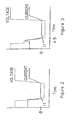
- timer circuitry (22) causes switch (15) to engage
- the voltage falls very rapidly to a reversed condition.
- the current falls quickly.
- Apparent in Figure 2 is an impulse of negative current (11) which may occur as the voltage reverses. This may be caused by the electron current flowing to discharge the target surface and thus help eliminate the uneven buildup of charge.
- Figure 3 shows how the same embodiment may react to a potential arc occurrence.
- the level of voltage falls (or the rate of change in the voltage may vary).
- this may be one aspect which gives rises to activation which in this embodiment causes a reversal of voltage as shown at time B.
- an impulse of negative current (11) may occur due to electron current flowing to discharge the target surface or the like to eliminate the uneven buildup of charge. In this situation, however, some increase in current is likely to occur as the arc begins to appear but before it is stopped by action of switch (15).
- the reversal may act as one way to eliminate the uneven buildup of charge within the plasma processing system. This uneven buildup may occur within plasma (5) or may occur on material target (6) or even on some other mask or other element within the processing system. The propensity to arc may also be the result of other anomalies.
- the current is not only immediately stopped, but the conditions giving rise to such a current may be negated. The plasma is thus restored to its net uniform distribution.
- typical recovery can occur as is known in the art. This may include ramping or reinstating the voltage as shown until current is restored and a steady state condition is resumed.
- the uneven build-up of charge may occur within plasma (5) or may occur on material target (6) or even on some other mask or other element within the processing system.
- the propensity to arc may also be the result of other anomalies.
- any such current is not only immediately stopped, but the conditions giving rise to such a current may be negated.
- the plasma is thus restored to its net uniform distribution.
- this uniform distribution or perhaps merely some processing advantages might be achieved in some systems in a variety of ways including merely interrupting the supply of power or voltage to the chamber. Since the processes are not fully understood, it should be understood that regardless of the reasons involved, advantages can be obtained by utilizing the techniques disclosed.
- this embodiment includes an inductor having first and second inductor portions (13 and 14) connected in series along first lead (8).
- first and second inductor portions (13 and 14) may be arranged in a variety of fashions and may even be designed in a transformer configuration.
- these first and second inductor portions (13 and 14) are magnetically coupled.
- a switch (15) is also connected in between first and second inductor portions (13 and 14) to second lead (9). This switch may be controlled by activation circuitry or, as shown directly by some sensor (17).
- sensor (17) may be triggered to act in a variety of ways to detect an arc condition as the actual presence or incipient presence of an are occurrence within plasma (5).
- switch (15) upon triggering of switch (15), the voltage applied across plasma (5) is immediately reversed as a result of the inductor being connected in series along first lead (8). This reversal may cause the immediate stoppage of current through plasma (5), may also act to clear the plasma of any uneven build-up of charge as discussed earlier, or may simply afford process advantages for unknown reasons. Voltage may naturally be reversed through a variety of other manners and still be considered an equivalent of the present invention including but not limited to supplying another power source output or switching to reverse voltage, and the like.
- second inductor portion (14) may not only be magnetically coupled to first inductor portion (13), but it may also have a turns ratio of at least about 10% of that of first inductor portion (13). In such a fashion, the turns ratio would dictate the magnitude of the reverse voltage. Since a substantial reverse voltage is desired (and in some instances either about 5% to 20% of the normal operating level or even 10V to 100V), a turns ratio of at least about 10% would achieve the goals mentioned earlier. Naturally other inductor geometries and even other components could be used in an equivalent fashion and would still fall within the scope of this patent.
- the reverse voltage be at least enough to quickly clear the undesirable condition, it may also not be so large as to risk reigniting an arc or to risk driving the plasma in a reverse mode and thereby quenching it.
- these limiting values will vary depending upon application, but for the applications presently contemplated, it is believed the limits discussed are adequate. Note that it is possible that some existing designs in other applications when acting to shut off a power source might achieve a slight voltage reversal. Even if applied to reactive sputtering, this slight voltage reversal is merely an incident of particular circuit designs and would not be the substantial voltage reversal involved for some aspects of the present invention as they achieve elimination of the uneven charge build-ups.
- switch (15) would be preferably of the non-latching type so as to allow easy opening of switch (15) to stop the reversal or other condition.
- switch (15) it has been found that integrated gate bipolar transistors, field effect transistors, darlington bipolar transistors and regular bipolar transistors are adequate, however, the integrated gate bipolar transistors affords easier control in the present configuration.
- the DC power source (1) may include an oscillator (18).
- Oscillator (18) might be merely some alternating power input or some means for accepting alternating power.
- the alternating power is at a predominant frequency and is converted through converter (19) into direct current power.
- a power supply switch (20) would then be included as known to create an alternating signal at a higher frequency. This alternating signal is then retransformed to a DC output through rectifier (21).
- FIG. 1 while some conceptual elements are shown within power supply switch (20) and rectifier (21) these are for visual understanding only.
- DC power source including first and second portions (13 and 14), switch (15), and a control means such as the sensor (17) and timer circuitry (22) shown and discussed earlier is included within DC power source (1).
- DC power source would not only supply a voltage, it would include a means for analyzing the output or a voltage and a means for immediately stopping current from flowing through its load.
- second inductor portion (14) and switch (15) this modified power source would include voltage reversal circuitry that can reverse the voltage to the load. Other such means are also possible including other configurations of merely some switch or even other power supply elements.
- switch (15) and timer circuitry (22), again regardless as to where configured or how achieved, might serve as interruption circuitry that interrupts the direct current power.
- no reverse voltage might occur, however, given proper system design, immediate stoppage of current through plasma (5) might occur or merely interrupting the supply of power or voltage might occur.
- the inclusion of first inductor portion (13) may still serve a valuable purpose.
- first inductor portion (13) such would be considered “large” within the context of this invention so long as the inductance of first inductor portion (13), when combined with the impedance of switch (15), and the power supply output impedance would result in a time constant sufficiently larger than the amount of time the switch would be engaged. As those skilled in the art would readily understand, this type of configuration would cause power supply to remain sufficiently loaded and unstressed throughout the time switch (15) were engaged.
- timer means (22) serves to engage switch (15) for the prescribed times.
- such a power source and system could be operated in a preventive mode through which plasma (5) could be periodically cleared of any uneven buildup of charged particles by applying a substantial reverse voltage.
- This periodic clearing occurs as frequently as every 10 microseconds to every 2000 microseconds, again, depending upon the particular process involved as discussed earlier.
- a means for periodically clearing plasma (5) is achieved as those skilled in the art would readily understand.
- other means for clearing the plasma could also be accomplished ranging from merely interrupting the supply of power, stopping the voltage, or even introducing other physical phenomena.
- one element is responsive to another element. This is meant in its broadest sense. For instance, since sensor means (17) detects conditions which ultimately cause some operation of switch (15), switch (15) should be deemed responsive to sensor means (17). This is in spite of the fact that the output may be filtered, transformed, or evaluated by another element such as a programmable processor and the like. Intermediate processing or manipulation would not impact this responsiveness. Similarly as those skilled in the art would understand, many steps in the techniques discussed can be accomplished at varying points in time, in varying orders, and even at external locations. Naturally each such variation would fall within the scope of this patent.
Landscapes
- Physics & Mathematics (AREA)
- Engineering & Computer Science (AREA)
- Plasma & Fusion (AREA)
- Chemical & Material Sciences (AREA)
- Analytical Chemistry (AREA)
- Plasma Technology (AREA)
- Physical Vapour Deposition (AREA)
- Lining And Supports For Tunnels (AREA)
Claims (11)
- Verfahren zur reakiven Katodenzerstäubung, bei dem ein Lichtbogen unterdrückt oder vermieden wird, umfassend das Zuführen eines leitenden Materialtargets (6), um in einer Beschichtungskammer (2) Beschichtungsmaterial freizusetzen, Zuführen wenigstens eines reaktiven Gases in die Beschichtungskammer, wobei das Gas mit dem Beschichtungsmaterial reagiert, um elektrisch isolierendes Material zu bilden, Zuführen von Gleichstromleistung durch Anlegen einer Gleichspannung in die Beschichtungskammer aus einer Gleichstromleistungsquelle, um ein aus geladenen Teilchen gebildetes Plasma (5) zu erzeugen, und Hervorrufen einer Ablagerung wenigstens eines Teils des elektrisch isolierenden Materials auf einem Substrat (7) durch die Wirkung des Plasmas; gekennzeichnet durch das periodische Umkehren der das Plasma erzeugenden Gleichspannung während einer Zeitspanne im Bereich zwischen 1 und 10 Mikrosekunden ohne Auslöschung des Plasmas, wobei die Umkehrung jeweils nach einer Zeit im Bereich von 10 Mikrosekunden bis 2000 Mikrosekunden durch Anlegen einer entgegengesetzten Spannung mit einem Pegel im Bereich zwischen 5 und 20 Prozent der Gleichspannung bewirkt wird.
- Verfahren nach Anspruch 1, bei dem die Größe der entgegengesetzten Spannung im Bereich zwischen 10 und 100 Volt liegt.
- Reaktives Plasma-Katodenzerstäubungssystem, bei dem ein Lichtbogen unterdrückt oder vermieden wird, mit einer Beschichtungskammer (2), einem leitenden Materialtarget (6), das so angeordnet ist, dass es Beschichtungsmaterial in der Kammer freisetzt, einer Versorgung für reaktives Gas, die mit der Beschichtungskammer verbunden ist, wobei das Gas mit dem Beschichtungsmaterial reagiert, um ein elektrisch isolierendes Material zu bilden, einer Anode (3), die in der Beschichtungskammer in der Nähe des Materialtargets (6) positioniert ist, und einer Gleichstromleistungsquelle (1), die an die Anode (3) und an das Materialtarget eine Gleichspannung anlegt und ein Plasma (5), das geladene Teilchen enthält, erzeugt, gekennzeichnet durch eine Zeitgeberschaltungsanordnung (22) und eine Spannungsumkehrschaltungsanordnung, die so betreibbar ist, dass sie die das Plasma erzeugende Gleichspannung für eine Zeitspanne im Bereich zwischen 1 und 10 Mikrosekunden jeweils nach einer Zeit im Bereich von 10 bis 2000 Mikrosekunden umkehrt, indem sie eine entgegengesetzte Spannung mit einem Pegel im Bereich zwischen 5 und 20 Prozent der Gleichspannung ohne Auslöschung des Plasmas anlegt, wobei die Spannungsumkehrschaltungsanordung auf die Zeitgeberschaltungsanordung anspricht.
- Reaktives Plasma-Katodenzerstäubungssystem nach Anspruch 3, ferner mit einem Sensor (17), auf den die Spannungsumkehrschaltungsanordung anspricht.
- Reaktives Plasma-Katodenzerstäubungssystem nach Anspruch 4, bei dem der Sensor (17) eine niedrige Ausgangsspannung der Gleichspannungsquelle erfasst.
- Reaktives Plasma-Katodenzerstäubungssystem nach Anspruch 4, bei dem der Sensor (17) eine hohe Änderungsrate der Ausgangsspannung der Gleichspannungsquelle erfasst.
- Reaktives Katodenzerstäubungssystem nach Anspruch 6, bei dem der Sensor außerdem eine niedrige Ausgangsspannung der Gleichspannungsquelle erfasst.
- Reaktives Plasma-Katodenzerstäubungssystem nach Anspruch 3, bei dem die Gleichspannungsquelle über eine erste Leitung (8) mit dem Materialtarget verbunden ist und über eine zweite Leitung (9) mit der Anode verbunden ist und bei dem die Spannungsumkehrschaltungsanordnung umfasst:a. einen Induktor (13, 14), der mit der ersten Leitung in Reihe geschaltet ist und einen ersten Induktorabschnitt (13) und einen zweiten Induktorabschnitt (14), die magnetisch gekoppelt sind, besitzt; undb. einen Schalter (15), der an einem Punkt zwischen dem ersten Induktorabschnitt und dem zweiten Induktorabschnitt zwischen die erste Leitung und die zweite Leitung geschaltet ist.
- Reaktives Plasma-Katodenzerstäubungssystem nach Anspruch 8, bei dem der Schalter (15) auf einen Sensor (17) anspricht.
- System nach Anspruch 8, bei dem die Induktivität des ersten Induktorabschnitts dann, wenn sie mit der Schalterimpedanz und mit der Leistungsversorgungs-Ausgangsimpedanz kombiniert wird, eine Zeitkonstante ergibt, die größer als die Zeitspanne ist, in der der Schalter geschlossen wäre.
- System nach Anspruch 10, bei dem das Wicklungsverhältnis des zweiten Induktorabschnitts zu dem ersten Induktorabschnitt wenigstens 10 Prozent beträgt.
Priority Applications (1)
| Application Number | Priority Date | Filing Date | Title |
|---|---|---|---|
| DE69433498.7T DE69433498T3 (de) | 1993-04-02 | 1994-04-01 | Reaktives gleichstrom-zerstäubungssystem |
Applications Claiming Priority (3)
| Application Number | Priority Date | Filing Date | Title |
|---|---|---|---|
| US42619 | 1993-04-02 | ||
| US08/042,619 US5718813A (en) | 1992-12-30 | 1993-04-02 | Enhanced reactive DC sputtering system |
| PCT/US1994/003611 WO1994023440A1 (en) | 1993-04-02 | 1994-04-01 | Reactive dc sputtering system |
Publications (3)
| Publication Number | Publication Date |
|---|---|
| EP0692138A1 EP0692138A1 (de) | 1996-01-17 |
| EP0692138B1 EP0692138B1 (de) | 2004-01-21 |
| EP0692138B2 true EP0692138B2 (de) | 2014-10-22 |
Family
ID=21922882
Family Applications (1)
| Application Number | Title | Priority Date | Filing Date |
|---|---|---|---|
| EP94912385.5A Expired - Lifetime EP0692138B2 (de) | 1993-04-02 | 1994-04-01 | Reaktives gleichstrom-zerstäubungssystem |
Country Status (6)
| Country | Link |
|---|---|
| US (3) | US5718813A (de) |
| EP (1) | EP0692138B2 (de) |
| JP (1) | JP3702304B2 (de) |
| AT (1) | ATE258337T1 (de) |
| DE (1) | DE69433498T3 (de) |
| WO (1) | WO1994023440A1 (de) |
Families Citing this family (153)
| Publication number | Priority date | Publication date | Assignee | Title |
|---|---|---|---|---|
| CH689767A5 (de) * | 1992-03-24 | 1999-10-15 | Balzers Hochvakuum | Verfahren zur Werkstueckbehandlung in einer Vakuumatmosphaere und Vakuumbehandlungsanlage. |
| US5718813A (en) * | 1992-12-30 | 1998-02-17 | Advanced Energy Industries, Inc. | Enhanced reactive DC sputtering system |
| US6217717B1 (en) | 1992-12-30 | 2001-04-17 | Advanced Energy Industries, Inc. | Periodically clearing thin film plasma processing system |
| SG74667A1 (en) * | 1993-07-28 | 2000-08-22 | Asahi Glass Co Ltd | Method of an apparatus for sputtering |
| JP3398447B2 (ja) | 1993-11-26 | 2003-04-21 | 新電元工業株式会社 | スパッタ装置用電源 |
| US5535906A (en) * | 1995-01-30 | 1996-07-16 | Advanced Energy Industries, Inc. | Multi-phase DC plasma processing system |
| WO1996031899A1 (en) * | 1995-04-07 | 1996-10-10 | Advanced Energy Industries, Inc. | Adjustable energy quantum thin film plasma processing system |
| US5917286A (en) | 1996-05-08 | 1999-06-29 | Advanced Energy Industries, Inc. | Pulsed direct current power supply configurations for generating plasmas |
| ATE468420T1 (de) | 1997-02-20 | 2010-06-15 | Shibaura Mechatronics Corp | Stromversorgungseinheit für sputtervorrichtung |
| SE9704607D0 (sv) * | 1997-12-09 | 1997-12-09 | Chemfilt R & D Ab | A method and apparatus for magnetically enhanced sputtering |
| IT1292295B1 (it) * | 1997-04-29 | 1999-01-29 | Sorin Biomedica Cardio Spa | Stent per angioplastica |
| US5897753A (en) * | 1997-05-28 | 1999-04-27 | Advanced Energy Industries, Inc. | Continuous deposition of insulating material using multiple anodes alternated between positive and negative voltages |
| US5993615A (en) * | 1997-06-19 | 1999-11-30 | International Business Machines Corporation | Method and apparatus for detecting arcs |
| US6276072B1 (en) * | 1997-07-10 | 2001-08-21 | Applied Materials, Inc. | Method and apparatus for heating and cooling substrates |
| TW460599B (en) * | 1998-01-14 | 2001-10-21 | Toshiba Corp | Method for forming fine wiring pattern |
| US7244677B2 (en) * | 1998-02-04 | 2007-07-17 | Semitool. Inc. | Method for filling recessed micro-structures with metallization in the production of a microelectronic device |
| WO1999040615A1 (en) | 1998-02-04 | 1999-08-12 | Semitool, Inc. | Method and apparatus for low-temperature annealing of metallization micro-structures in the production of a microelectronic device |
| US6632292B1 (en) * | 1998-03-13 | 2003-10-14 | Semitool, Inc. | Selective treatment of microelectronic workpiece surfaces |
| US6416647B1 (en) | 1998-04-21 | 2002-07-09 | Applied Materials, Inc. | Electro-chemical deposition cell for face-up processing of single semiconductor substrates |
| DE69929967T2 (de) | 1998-04-21 | 2007-05-24 | Applied Materials, Inc., Santa Clara | Elektroplattierungssystem und verfahren zur elektroplattierung auf substraten |
| US6113771A (en) * | 1998-04-21 | 2000-09-05 | Applied Materials, Inc. | Electro deposition chemistry |
| US6994776B2 (en) * | 1998-06-01 | 2006-02-07 | Semitool Inc. | Method and apparatus for low temperature annealing of metallization micro-structure in the production of a microelectronic device |
| US6287977B1 (en) * | 1998-07-31 | 2001-09-11 | Applied Materials, Inc. | Method and apparatus for forming improved metal interconnects |
| US6290865B1 (en) | 1998-11-30 | 2001-09-18 | Applied Materials, Inc. | Spin-rinse-drying process for electroplated semiconductor wafers |
| US6258220B1 (en) | 1998-11-30 | 2001-07-10 | Applied Materials, Inc. | Electro-chemical deposition system |
| US6228233B1 (en) | 1998-11-30 | 2001-05-08 | Applied Materials, Inc. | Inflatable compliant bladder assembly |
| US6254760B1 (en) | 1999-03-05 | 2001-07-03 | Applied Materials, Inc. | Electro-chemical deposition system and method |
| US6544399B1 (en) | 1999-01-11 | 2003-04-08 | Applied Materials, Inc. | Electrodeposition chemistry for filling apertures with reflective metal |
| US6379522B1 (en) | 1999-01-11 | 2002-04-30 | Applied Materials, Inc. | Electrodeposition chemistry for filling of apertures with reflective metal |
| US7192494B2 (en) * | 1999-03-05 | 2007-03-20 | Applied Materials, Inc. | Method and apparatus for annealing copper films |
| US6136163A (en) * | 1999-03-05 | 2000-10-24 | Applied Materials, Inc. | Apparatus for electro-chemical deposition with thermal anneal chamber |
| KR100302457B1 (ko) | 1999-04-06 | 2001-10-29 | 박호군 | 다이아몬드 막 증착방법 |
| US6551488B1 (en) * | 1999-04-08 | 2003-04-22 | Applied Materials, Inc. | Segmenting of processing system into wet and dry areas |
| US6557237B1 (en) | 1999-04-08 | 2003-05-06 | Applied Materials, Inc. | Removable modular cell for electro-chemical plating and method |
| US6837978B1 (en) | 1999-04-08 | 2005-01-04 | Applied Materials, Inc. | Deposition uniformity control for electroplating apparatus, and associated method |
| US6582578B1 (en) | 1999-04-08 | 2003-06-24 | Applied Materials, Inc. | Method and associated apparatus for tilting a substrate upon entry for metal deposition |
| US6571657B1 (en) | 1999-04-08 | 2003-06-03 | Applied Materials Inc. | Multiple blade robot adjustment apparatus and associated method |
| US6551484B2 (en) | 1999-04-08 | 2003-04-22 | Applied Materials, Inc. | Reverse voltage bias for electro-chemical plating system and method |
| US6662673B1 (en) | 1999-04-08 | 2003-12-16 | Applied Materials, Inc. | Linear motion apparatus and associated method |
| US6585876B2 (en) | 1999-04-08 | 2003-07-01 | Applied Materials Inc. | Flow diffuser to be used in electro-chemical plating system and method |
| US6451389B1 (en) * | 1999-04-17 | 2002-09-17 | Advanced Energy Industries, Inc. | Method for deposition of diamond like carbon |
| US6516815B1 (en) | 1999-07-09 | 2003-02-11 | Applied Materials, Inc. | Edge bead removal/spin rinse dry (EBR/SRD) module |
| US20030213772A9 (en) * | 1999-07-09 | 2003-11-20 | Mok Yeuk-Fai Edwin | Integrated semiconductor substrate bevel cleaning apparatus and method |
| US6818103B1 (en) | 1999-10-15 | 2004-11-16 | Advanced Energy Industries, Inc. | Method and apparatus for substrate biasing in multiple electrode sputtering systems |
| US6193855B1 (en) | 1999-10-19 | 2001-02-27 | Applied Materials, Inc. | Use of modulated inductive power and bias power to reduce overhang and improve bottom coverage |
| US6350353B2 (en) | 1999-11-24 | 2002-02-26 | Applied Materials, Inc. | Alternate steps of IMP and sputtering process to improve sidewall coverage |
| JP5054874B2 (ja) * | 1999-12-02 | 2012-10-24 | ティーガル コーポレイション | リアクタ内でプラチナエッチングを行う方法 |
| US6344419B1 (en) | 1999-12-03 | 2002-02-05 | Applied Materials, Inc. | Pulsed-mode RF bias for sidewall coverage improvement |
| DE10015244C2 (de) * | 2000-03-28 | 2002-09-19 | Fraunhofer Ges Forschung | Verfahren und Schaltungsanordnung zur pulsförmigen Energieeinspeisung in Magnetronentladungen |
| US6554979B2 (en) | 2000-06-05 | 2003-04-29 | Applied Materials, Inc. | Method and apparatus for bias deposition in a modulating electric field |
| US20040079633A1 (en) * | 2000-07-05 | 2004-04-29 | Applied Materials, Inc. | Apparatus for electro chemical deposition of copper metallization with the capability of in-situ thermal annealing |
| US6576110B2 (en) | 2000-07-07 | 2003-06-10 | Applied Materials, Inc. | Coated anode apparatus and associated method |
| US20020112964A1 (en) * | 2000-07-12 | 2002-08-22 | Applied Materials, Inc. | Process window for gap-fill on very high aspect ratio structures using additives in low acid copper baths |
| US6524455B1 (en) * | 2000-10-04 | 2003-02-25 | Eni Technology, Inc. | Sputtering apparatus using passive arc control system and method |
| US6610189B2 (en) | 2001-01-03 | 2003-08-26 | Applied Materials, Inc. | Method and associated apparatus to mechanically enhance the deposition of a metal film within a feature |
| US6478937B2 (en) | 2001-01-19 | 2002-11-12 | Applied Material, Inc. | Substrate holder system with substrate extension apparatus and associated method |
| JP2002324875A (ja) * | 2001-04-26 | 2002-11-08 | Fuji Photo Film Co Ltd | 半導体パッケージ基台および半導体パッケージ |
| GB0116688D0 (en) * | 2001-07-07 | 2001-08-29 | Trikon Holdings Ltd | Method of depositing aluminium nitride |
| US7469558B2 (en) * | 2001-07-10 | 2008-12-30 | Springworks, Llc | As-deposited planar optical waveguides with low scattering loss and methods for their manufacture |
| US6746591B2 (en) | 2001-10-16 | 2004-06-08 | Applied Materials Inc. | ECP gap fill by modulating the voltate on the seed layer to increase copper concentration inside feature |
| US7404877B2 (en) * | 2001-11-09 | 2008-07-29 | Springworks, Llc | Low temperature zirconia based thermal barrier layer by PVD |
| US6824612B2 (en) | 2001-12-26 | 2004-11-30 | Applied Materials, Inc. | Electroless plating system |
| US6770565B2 (en) | 2002-01-08 | 2004-08-03 | Applied Materials Inc. | System for planarizing metal conductive layers |
| US20030146102A1 (en) * | 2002-02-05 | 2003-08-07 | Applied Materials, Inc. | Method for forming copper interconnects |
| US7378356B2 (en) * | 2002-03-16 | 2008-05-27 | Springworks, Llc | Biased pulse DC reactive sputtering of oxide films |
| US20030175142A1 (en) * | 2002-03-16 | 2003-09-18 | Vassiliki Milonopoulou | Rare-earth pre-alloyed PVD targets for dielectric planar applications |
| US6884327B2 (en) | 2002-03-16 | 2005-04-26 | Tao Pan | Mode size converter for a planar waveguide |
| US8431264B2 (en) * | 2002-08-09 | 2013-04-30 | Infinite Power Solutions, Inc. | Hybrid thin-film battery |
| US8445130B2 (en) * | 2002-08-09 | 2013-05-21 | Infinite Power Solutions, Inc. | Hybrid thin-film battery |
| US8236443B2 (en) * | 2002-08-09 | 2012-08-07 | Infinite Power Solutions, Inc. | Metal film encapsulation |
| US8394522B2 (en) * | 2002-08-09 | 2013-03-12 | Infinite Power Solutions, Inc. | Robust metal film encapsulation |
| US7993773B2 (en) | 2002-08-09 | 2011-08-09 | Infinite Power Solutions, Inc. | Electrochemical apparatus with barrier layer protected substrate |
| US20070264564A1 (en) | 2006-03-16 | 2007-11-15 | Infinite Power Solutions, Inc. | Thin film battery on an integrated circuit or circuit board and method thereof |
| US8404376B2 (en) | 2002-08-09 | 2013-03-26 | Infinite Power Solutions, Inc. | Metal film encapsulation |
| US8021778B2 (en) * | 2002-08-09 | 2011-09-20 | Infinite Power Solutions, Inc. | Electrochemical apparatus with barrier layer protected substrate |
| AU2003261463A1 (en) * | 2002-08-27 | 2004-03-19 | Symmorphix, Inc. | Optically coupling into highly uniform waveguides |
| US7147759B2 (en) * | 2002-09-30 | 2006-12-12 | Zond, Inc. | High-power pulsed magnetron sputtering |
| US6853142B2 (en) * | 2002-11-04 | 2005-02-08 | Zond, Inc. | Methods and apparatus for generating high-density plasma |
| US6896773B2 (en) * | 2002-11-14 | 2005-05-24 | Zond, Inc. | High deposition rate sputtering |
| US7138039B2 (en) * | 2003-01-21 | 2006-11-21 | Applied Materials, Inc. | Liquid isolation of contact rings |
| US7087144B2 (en) * | 2003-01-31 | 2006-08-08 | Applied Materials, Inc. | Contact ring with embedded flexible contacts |
| US7025861B2 (en) * | 2003-02-06 | 2006-04-11 | Applied Materials | Contact plating apparatus |
| US7205662B2 (en) | 2003-02-27 | 2007-04-17 | Symmorphix, Inc. | Dielectric barrier layer films |
| US7311810B2 (en) * | 2003-04-18 | 2007-12-25 | Applied Materials, Inc. | Two position anneal chamber |
| US20040206628A1 (en) * | 2003-04-18 | 2004-10-21 | Applied Materials, Inc. | Electrical bias during wafer exit from electrolyte bath |
| US7238628B2 (en) * | 2003-05-23 | 2007-07-03 | Symmorphix, Inc. | Energy conversion and storage films and devices by physical vapor deposition of titanium and titanium oxides and sub-oxides |
| US8728285B2 (en) * | 2003-05-23 | 2014-05-20 | Demaray, Llc | Transparent conductive oxides |
| US6967305B2 (en) * | 2003-08-18 | 2005-11-22 | Mks Instruments, Inc. | Control of plasma transitions in sputter processing systems |
| US6995545B2 (en) * | 2003-08-18 | 2006-02-07 | Mks Instruments, Inc. | Control system for a sputtering system |
| US20050092602A1 (en) * | 2003-10-29 | 2005-05-05 | Harald Herchen | Electrochemical plating cell having a membrane stack |
| US20050092601A1 (en) * | 2003-10-29 | 2005-05-05 | Harald Herchen | Electrochemical plating cell having a diffusion member |
| US20050103620A1 (en) * | 2003-11-19 | 2005-05-19 | Zond, Inc. | Plasma source with segmented magnetron cathode |
| US9771648B2 (en) * | 2004-08-13 | 2017-09-26 | Zond, Inc. | Method of ionized physical vapor deposition sputter coating high aspect-ratio structures |
| US9123508B2 (en) * | 2004-02-22 | 2015-09-01 | Zond, Llc | Apparatus and method for sputtering hard coatings |
| US7095179B2 (en) * | 2004-02-22 | 2006-08-22 | Zond, Inc. | Methods and apparatus for generating strongly-ionized plasmas with ionizational instabilities |
| DE102004015090A1 (de) | 2004-03-25 | 2005-11-03 | Hüttinger Elektronik Gmbh + Co. Kg | Bogenentladungserkennungseinrichtung |
| US20050218000A1 (en) * | 2004-04-06 | 2005-10-06 | Applied Materials, Inc. | Conditioning of contact leads for metal plating systems |
| US7285195B2 (en) * | 2004-06-24 | 2007-10-23 | Applied Materials, Inc. | Electric field reducing thrust plate |
| US6943317B1 (en) | 2004-07-02 | 2005-09-13 | Advanced Energy Industries, Inc. | Apparatus and method for fast arc extinction with early shunting of arc current in plasma |
| EP2477207A3 (de) * | 2004-09-24 | 2014-09-03 | Zond, Inc. | Vorrichtung zum Erzeugen von elektrischen Hochstrom-entladungen |
| US20060102467A1 (en) * | 2004-11-15 | 2006-05-18 | Harald Herchen | Current collimation for thin seed and direct plating |
| KR101127370B1 (ko) * | 2004-12-08 | 2012-03-29 | 인피니트 파워 솔루션스, 인크. | LiCoO2의 증착 |
| US7959769B2 (en) * | 2004-12-08 | 2011-06-14 | Infinite Power Solutions, Inc. | Deposition of LiCoO2 |
| US7372610B2 (en) | 2005-02-23 | 2008-05-13 | Sage Electrochromics, Inc. | Electrochromic devices and methods |
| US7305311B2 (en) * | 2005-04-22 | 2007-12-04 | Advanced Energy Industries, Inc. | Arc detection and handling in radio frequency power applications |
| US20060283702A1 (en) * | 2005-06-21 | 2006-12-21 | Applied Materials, Inc. | Random pulsed DC power supply |
| US20070014958A1 (en) * | 2005-07-08 | 2007-01-18 | Chaplin Ernest R | Hanger labels, label assemblies and methods for forming the same |
| US20070048451A1 (en) * | 2005-08-26 | 2007-03-01 | Applied Materials, Inc. | Substrate movement and process chamber scheduling |
| US7432184B2 (en) * | 2005-08-26 | 2008-10-07 | Applied Materials, Inc. | Integrated PVD system using designated PVD chambers |
| US7838133B2 (en) * | 2005-09-02 | 2010-11-23 | Springworks, Llc | Deposition of perovskite and other compound ceramic films for dielectric applications |
| DE502005006550D1 (de) * | 2005-12-22 | 2009-03-12 | Huettinger Elektronik Gmbh | Verfahren und Vorrichtung zur Arcerkennung in einem Plasmaprozess |
| US7445695B2 (en) * | 2006-04-28 | 2008-11-04 | Advanced Energy Industries Inc. | Method and system for conditioning a vapor deposition target |
| US7514935B2 (en) * | 2006-09-13 | 2009-04-07 | Advanced Energy Industries, Inc. | System and method for managing power supplied to a plasma chamber |
| DE102006043900B4 (de) * | 2006-09-19 | 2008-09-18 | Siemens Ag | Vorrichtung und Verfahren zum Betrieb einer Plasmaanlage |
| DE102006043898A1 (de) * | 2006-09-19 | 2008-04-17 | Siemens Ag | Vorrichtung und Verfahren zum Betrieb einer Plasmaanlage |
| CN101523571A (zh) * | 2006-09-29 | 2009-09-02 | 无穷动力解决方案股份有限公司 | 柔性基板上沉积的电池层的掩模和材料限制 |
| US8197781B2 (en) * | 2006-11-07 | 2012-06-12 | Infinite Power Solutions, Inc. | Sputtering target of Li3PO4 and method for producing same |
| DE502006005363D1 (de) * | 2006-11-23 | 2009-12-24 | Huettinger Elektronik Gmbh | Verfahren zum Erkennen einer Bogenentladung in einem Plasmaprozess und Bogenentladungserkennungsvorrichtung |
| US7795817B2 (en) * | 2006-11-24 | 2010-09-14 | Huettinger Elektronik Gmbh + Co. Kg | Controlled plasma power supply |
| EP1928009B1 (de) * | 2006-11-28 | 2013-04-10 | HÜTTINGER Elektronik GmbH + Co. KG | Bogenentladungs-Erkennungseinrichtung, Plasma-Leistungsversorgung und Verfahren zum Erkennen von Bogenentladungen |
| EP2102889B1 (de) * | 2006-12-12 | 2020-10-07 | Evatec AG | Hf-substrat-bias mit hochleistungs-impulsmagnetronsputterung (hipims) |
| DE502006009308D1 (de) * | 2006-12-14 | 2011-05-26 | Huettinger Elektronik Gmbh | Bogenentladungs-Erkennungseinrichtung, Plasma-Leistungsversorgung und Verfahren zum Erkennen von Bogenentladungen |
| US8217299B2 (en) * | 2007-02-22 | 2012-07-10 | Advanced Energy Industries, Inc. | Arc recovery without over-voltage for plasma chamber power supplies using a shunt switch |
| EP1978542B1 (de) | 2007-03-08 | 2010-12-29 | HÜTTINGER Elektronik GmbH + Co. KG | Verfahren und Vorrichtung zum Unterdrücken von Bogenentladungen beim Betreiben eines Plasmaprozesses |
| EP1995818A1 (de) * | 2007-05-12 | 2008-11-26 | Huettinger Electronic Sp. z o. o | Schaltung und Verfahren zur Reduzierung der in einer Zuleitungsinduktivität gespeicherten elektrischen Energie zur schnellen Plasmalichtbogenlöschung |
| US8133359B2 (en) | 2007-11-16 | 2012-03-13 | Advanced Energy Industries, Inc. | Methods and apparatus for sputtering deposition using direct current |
| US9039871B2 (en) | 2007-11-16 | 2015-05-26 | Advanced Energy Industries, Inc. | Methods and apparatus for applying periodic voltage using direct current |
| US8268488B2 (en) | 2007-12-21 | 2012-09-18 | Infinite Power Solutions, Inc. | Thin film electrolyte for thin film batteries |
| CN101903560B (zh) * | 2007-12-21 | 2014-08-06 | 无穷动力解决方案股份有限公司 | 用于电解质膜的溅射靶的方法 |
| ATE547804T1 (de) * | 2007-12-24 | 2012-03-15 | Huettinger Electronic Sp Z O O | Stromänderungsbegrenzungsvorrichtung |
| US8518581B2 (en) | 2008-01-11 | 2013-08-27 | Inifinite Power Solutions, Inc. | Thin film encapsulation for thin film batteries and other devices |
| WO2009124191A2 (en) * | 2008-04-02 | 2009-10-08 | Infinite Power Solutions, Inc. | Passive over/under voltage control and protection for energy storage devices associated with energy harvesting |
| WO2009134756A1 (en) * | 2008-04-29 | 2009-11-05 | Cirrus Logic, Inc. | Cascaded switching power converter for coupling a photovoltaic energy source to power mains |
| US8158017B2 (en) * | 2008-05-12 | 2012-04-17 | Lam Research Corporation | Detection of arcing events in wafer plasma processing through monitoring of trace gas concentrations |
| US8044594B2 (en) * | 2008-07-31 | 2011-10-25 | Advanced Energy Industries, Inc. | Power supply ignition system and method |
| JP2012500610A (ja) | 2008-08-11 | 2012-01-05 | インフィニット パワー ソリューションズ, インコーポレイテッド | 電磁エネルギー獲得ための統合コレクタ表面を有するエネルギーデバイスおよびその方法 |
| CN102150185B (zh) * | 2008-09-12 | 2014-05-28 | 无穷动力解决方案股份有限公司 | 具有经由电磁能进行数据通信的组成导电表面的能量装置及其方法 |
| WO2010042594A1 (en) * | 2008-10-08 | 2010-04-15 | Infinite Power Solutions, Inc. | Environmentally-powered wireless sensor module |
| US20110236591A1 (en) * | 2008-11-28 | 2011-09-29 | General Plasma Inc. | Bipolar rectifier power supply |
| US8395078B2 (en) | 2008-12-05 | 2013-03-12 | Advanced Energy Industries, Inc | Arc recovery with over-voltage protection for plasma-chamber power supplies |
| EP2648209B1 (de) | 2009-02-17 | 2018-01-03 | Solvix GmbH | Energieversorgungsvorrichtung zur Plasmaverarbeitung |
| CN102439778B (zh) * | 2009-05-20 | 2016-02-10 | 萨普拉斯特研究有限责任公司 | 用于将电化学器件集成到固定设施之内或之上的方法 |
| CN102576828B (zh) | 2009-09-01 | 2016-04-20 | 萨普拉斯特研究有限责任公司 | 具有集成薄膜电池的印刷电路板 |
| US8968535B2 (en) * | 2009-12-14 | 2015-03-03 | Spp Process Technology Systems Uk Limited | Ion beam source |
| EP2577777B1 (de) | 2010-06-07 | 2016-12-28 | Sapurast Research LLC | Wiederaufladbare elektrochemische vorrichtung von hoher dichte |
| EP2410555A1 (de) * | 2010-07-19 | 2012-01-25 | Applied Materials, Inc. | Vorrichtung und Verfahren zur Zustandsbestimmung eines Beschichtungsgeräts |
| US8552665B2 (en) | 2010-08-20 | 2013-10-08 | Advanced Energy Industries, Inc. | Proactive arc management of a plasma load |
| US9263241B2 (en) | 2011-05-10 | 2016-02-16 | Advanced Energy Industries, Inc. | Current threshold response mode for arc management |
| EP3035365A1 (de) * | 2014-12-19 | 2016-06-22 | TRUMPF Huettinger Sp. Z o. o. | Verfahren zur Erfassung eines Lichtbogens während der Energieversorgung eines Plasmaverfahrens, Steuereinheit für eine Plasma-Energieversorgung und Plasma-Energieversorgung |
| US11049702B2 (en) | 2015-04-27 | 2021-06-29 | Advanced Energy Industries, Inc. | Rate enhanced pulsed DC sputtering system |
| US9812305B2 (en) | 2015-04-27 | 2017-11-07 | Advanced Energy Industries, Inc. | Rate enhanced pulsed DC sputtering system |
| US10373811B2 (en) | 2015-07-24 | 2019-08-06 | Aes Global Holdings, Pte. Ltd | Systems and methods for single magnetron sputtering |
| KR102361417B1 (ko) * | 2017-09-26 | 2022-02-09 | 어드밴스드 에너지 인더스트리즈 인코포레이티드 | 플라즈마 점화를 위한 시스템 및 방법 |
Citations (2)
| Publication number | Priority date | Publication date | Assignee | Title |
|---|---|---|---|---|
| US4046659A (en) † | 1974-05-10 | 1977-09-06 | Airco, Inc. | Method for coating a substrate |
| JPH02141572A (ja) † | 1988-11-24 | 1990-05-30 | Hitachi Ltd | バイアススパツタリング法および装置 |
Family Cites Families (59)
| Publication number | Priority date | Publication date | Assignee | Title |
|---|---|---|---|---|
| DE221202C (de) * | ||||
| DE229160C (de) * | ||||
| GB1134562A (en) * | 1965-06-30 | 1968-11-27 | Edwards High Vacuum Int Ltd | Methods of preventing localised arcing within the evacuated chamber of electrical discharge apparatus |
| DE2422808A1 (de) * | 1974-05-10 | 1975-11-20 | Leybold Heraeus Gmbh & Co Kg | Verfahren und anordnung zur leistungssteuerung eines hochfrequenz-generators fuer katodenzerstaeubungsanlagen |
| US4103324A (en) * | 1976-12-22 | 1978-07-25 | Airco, Inc. | Saturable reactor-type power supply |
| FR2379615A1 (fr) * | 1977-02-08 | 1978-09-01 | Vide & Traitement Sa | Procede de traitement thermochimique de metaux |
| JPS5458636A (en) * | 1977-10-20 | 1979-05-11 | Kawasaki Heavy Ind Ltd | Ion nitriding method |
| BG29362A1 (en) * | 1979-03-11 | 1980-11-14 | Minchev | Apparatus for chemical- thermal processing of matal articles in the condition of electrical smouldering charge |
| JPS5769324A (en) * | 1980-10-11 | 1982-04-28 | Daiwa Dengiyou Kk | Monitor device of dc power supply |
| DE3121389A1 (de) * | 1980-12-03 | 1982-08-19 | Kombinat Veb Keramische Werke Hermsdorf, Ddr 6530 Hermsdorf | Verfahren zum vorsputtern von targets in plasmatron-zerstaeubungsanlagen |
| US4396478A (en) * | 1981-06-15 | 1983-08-02 | Aizenshtein Anatoly G | Method of control of chemico-thermal treatment of workpieces in glow discharge and a device for carrying out the method |
| DD221202A1 (de) * | 1983-12-15 | 1985-04-17 | Fi Manfred V Ardenne | Einrichtung zur verhinderung von ueberschlaegen beim hochratezerstaeuben |
| DD229160B1 (de) * | 1984-04-16 | 1989-11-29 | Adw Ddr | Schaltungsanordnung zum betreiben von gleichstromplasmatronzerstaeubungsvorrichtungen |
| JPS6130665A (ja) * | 1984-07-20 | 1986-02-12 | Anelva Corp | スパツタ装置 |
| BG41745A1 (en) * | 1984-12-29 | 1987-08-14 | Minchev | Device for discontinuing of arc dicharges in gas dicharge vessel |
| US4711767A (en) * | 1985-02-05 | 1987-12-08 | Psi Star | Plasma reactor with voltage transformer |
| US4610775A (en) * | 1985-07-26 | 1986-09-09 | Westinghouse Electric Corp. | Method and apparatus for clearing short-circuited, high-voltage cathodes in a sputtering chamber |
| US4693805A (en) * | 1986-02-14 | 1987-09-15 | Boe Limited | Method and apparatus for sputtering a dielectric target or for reactive sputtering |
| US4710694A (en) * | 1986-06-02 | 1987-12-01 | Acme Electric Corporation | Microprocessor controlled battery charger |
| DE3700633C2 (de) * | 1987-01-12 | 1997-02-20 | Reinar Dr Gruen | Verfahren und Vorrichtung zum schonenden Beschichten elektrisch leitender Gegenstände mittels Plasma |
| JPS63190168A (ja) * | 1987-01-30 | 1988-08-05 | Sumitomo Electric Ind Ltd | 薄膜製造装置の電源装置 |
| ATE83269T1 (de) * | 1987-04-06 | 1992-12-15 | Filteco Spa | Verfahren und vorrichtung zur herstellung von polypropylenfaeden. |
| DE3821207A1 (de) * | 1988-06-23 | 1989-12-28 | Leybold Ag | Anordnung zum beschichten eines substrats mit dielektrika |
| GB8817684D0 (en) * | 1988-07-25 | 1988-09-01 | Astec Int Ltd | Power factor improvement |
| US4936960A (en) * | 1989-01-03 | 1990-06-26 | Advanced Energy Industries, Inc. | Method and apparatus for recovery from low impedance condition during cathodic arc processes |
| US5009764A (en) * | 1989-01-13 | 1991-04-23 | Advanced Energy Industries, Inc. | Apparatus for removal of electrical shorts in a sputtering system |
| US4963238A (en) * | 1989-01-13 | 1990-10-16 | Siefkes Jerry D | Method for removal of electrical shorts in a sputtering system |
| JPH02192698A (ja) * | 1989-01-19 | 1990-07-30 | Toshiba Corp | X線高電圧装置 |
| FR2648001B1 (fr) * | 1989-05-31 | 1991-09-27 | Breda Jean Pierre | Alimentation en courant continu d'electrodes a plasma et procede pour regenerer un plasma |
| DE3919145A1 (de) * | 1989-06-12 | 1990-12-13 | Leybold Ag | Verfahren und vorrichtung zum beschichten eines substrats mit elektrisch leitenden werkstoffen |
| DE3919147C2 (de) * | 1989-06-12 | 1998-01-15 | Leybold Ag | Verfahren zum Beschichten eines Kunststoffsubstrats mit Aluminium |
| JPH0356671A (ja) * | 1989-07-21 | 1991-03-12 | Fujitsu Ltd | スパッタリング装置 |
| JPH0361368A (ja) * | 1989-07-28 | 1991-03-18 | Hitachi Nakaseiki Ltd | イオンスパッタリング方法およびその装置 |
| DE3925536A1 (de) * | 1989-08-02 | 1991-02-07 | Leybold Ag | Anordnung zur dickenmessung von duennschichten |
| DE3926877A1 (de) * | 1989-08-16 | 1991-02-21 | Leybold Ag | Verfahren zum beschichten eines dielektrischen substrats mit kupfer |
| DE3934092A1 (de) * | 1989-10-12 | 1991-04-18 | Leybold Ag | Vorrichtung zum beschichten eines kunststoffsubstrats, vorzugsweise eines polymethylmethacrylat-substrats mit aluminium |
| US5241152A (en) * | 1990-03-23 | 1993-08-31 | Anderson Glen L | Circuit for detecting and diverting an electrical arc in a glow discharge apparatus |
| US5212425A (en) * | 1990-10-10 | 1993-05-18 | Hughes Aircraft Company | Ion implantation and surface processing method and apparatus |
| US5126033A (en) * | 1990-12-31 | 1992-06-30 | Leybold Aktiengesellschaft | Process and apparatus for reactively coating a substrate |
| US5138513A (en) * | 1991-01-23 | 1992-08-11 | Ransburg Corporation | Arc preventing electrostatic power supply |
| DE4113704A1 (de) * | 1991-04-26 | 1992-10-29 | Physikalisch Tech I | Schaltungsanordnung zur vermeidung der einfluesse von bogenentladungen bei reaktiven dc-hochratezerstaeuben |
| US5357418A (en) * | 1991-05-02 | 1994-10-18 | Robert Clavel | Hybrid power supply for converting an alternating input signal into a direct output signal |
| DE9109503U1 (de) * | 1991-07-31 | 1991-10-17 | Magtron Magneto Elektronische Geraete Gmbh, 7583 Ottersweier | Schaltungsanordnung für ein Stromversorgungsgerät für Geräte und Anlagen der Plasma- und Oberflächentechnik |
| DE4127317C2 (de) * | 1991-08-17 | 1999-09-02 | Leybold Ag | Einrichtung zum Behandeln von Substraten |
| US5281321A (en) * | 1991-08-20 | 1994-01-25 | Leybold Aktiengesellschaft | Device for the suppression of arcs |
| DE4127504A1 (de) * | 1991-08-20 | 1993-02-25 | Leybold Ag | Einrichtung zur unterdrueckung von lichtboegen |
| DE4127505C2 (de) * | 1991-08-20 | 2003-05-08 | Unaxis Deutschland Holding | Einrichtung zur Unterdrückung von Lichtbögen in Gasentladungsvorrichtungen |
| DE4202425C2 (de) * | 1992-01-29 | 1997-07-17 | Leybold Ag | Verfahren und Vorrichtung zum Beschichten eines Substrats, insbesondere mit elektrisch nichtleitenden Schichten |
| JPH06145975A (ja) * | 1992-03-20 | 1994-05-27 | Komag Inc | 炭素フィルムをスパタリングする方法及びその製造物 |
| CH689767A5 (de) * | 1992-03-24 | 1999-10-15 | Balzers Hochvakuum | Verfahren zur Werkstueckbehandlung in einer Vakuumatmosphaere und Vakuumbehandlungsanlage. |
| JP3071298B2 (ja) * | 1992-04-27 | 2000-07-31 | 株式会社ニコン | 反応性直流スパッタリングによる薄膜の製造方法 |
| DE69303853T2 (de) * | 1992-04-27 | 1996-12-12 | Central Glass Co Ltd | Verfahren zur Bildung einer Dünnschicht auf einem Substrat mittels reaktiven Gleichstrom-Sputtern |
| DE4233720C2 (de) * | 1992-10-07 | 2001-05-17 | Leybold Ag | Einrichtung für die Verhinderung von Überschlägen in Vakuum-Zerstäubungsanlagen |
| DE4237517A1 (de) * | 1992-11-06 | 1994-05-11 | Leybold Ag | Vorrichtung zum Beschichten eines Substrats, insbesondere mit elektrisch nichtleitenden Schichten |
| US5427669A (en) * | 1992-12-30 | 1995-06-27 | Advanced Energy Industries, Inc. | Thin film DC plasma processing system |
| US5718813A (en) * | 1992-12-30 | 1998-02-17 | Advanced Energy Industries, Inc. | Enhanced reactive DC sputtering system |
| US5478456A (en) * | 1993-10-01 | 1995-12-26 | Minnesota Mining And Manufacturing Company | Sputtering target |
| US5549795A (en) * | 1994-08-25 | 1996-08-27 | Hughes Aircraft Company | Corona source for producing corona discharge and fluid waste treatment with corona discharge |
| JP3056671U (ja) | 1998-08-11 | 1999-02-26 | 株式会社フジサワ | 着脱自在な時計 |
-
1993
- 1993-04-02 US US08/042,619 patent/US5718813A/en not_active Expired - Lifetime
-
1994
- 1994-04-01 EP EP94912385.5A patent/EP0692138B2/de not_active Expired - Lifetime
- 1994-04-01 WO PCT/US1994/003611 patent/WO1994023440A1/en not_active Ceased
- 1994-04-01 AT AT94912385T patent/ATE258337T1/de not_active IP Right Cessation
- 1994-04-01 JP JP52241694A patent/JP3702304B2/ja not_active Expired - Fee Related
- 1994-04-01 DE DE69433498.7T patent/DE69433498T3/de not_active Expired - Lifetime
-
1995
- 1995-09-29 US US08/532,559 patent/US6001224A/en not_active Expired - Fee Related
-
1998
- 1998-02-17 US US09/024,247 patent/US6024844A/en not_active Expired - Lifetime
Patent Citations (2)
| Publication number | Priority date | Publication date | Assignee | Title |
|---|---|---|---|---|
| US4046659A (en) † | 1974-05-10 | 1977-09-06 | Airco, Inc. | Method for coating a substrate |
| JPH02141572A (ja) † | 1988-11-24 | 1990-05-30 | Hitachi Ltd | バイアススパツタリング法および装置 |
Non-Patent Citations (1)
| Title |
|---|
| SOCIETY OF VACUUM COATERS: "35th Annual Technical Conference proceedings", 1992, article R.A. SCHOLL: "Process improvements for sputtering carbon and other difficult materials using combined AC and DC process power", pages: 391 - 394 † |
Also Published As
| Publication number | Publication date |
|---|---|
| US6024844A (en) | 2000-02-15 |
| DE69433498T3 (de) | 2015-02-19 |
| EP0692138B1 (de) | 2004-01-21 |
| ATE258337T1 (de) | 2004-02-15 |
| DE69433498D1 (de) | 2004-02-26 |
| EP0692138A1 (de) | 1996-01-17 |
| DE69433498T2 (de) | 2004-11-04 |
| JP3702304B2 (ja) | 2005-10-05 |
| US6001224A (en) | 1999-12-14 |
| US5718813A (en) | 1998-02-17 |
| WO1994023440A1 (en) | 1994-10-13 |
| JPH08510504A (ja) | 1996-11-05 |
Similar Documents
| Publication | Publication Date | Title |
|---|---|---|
| EP0692138B2 (de) | Reaktives gleichstrom-zerstäubungssystem | |
| EP0628212B1 (de) | Gleichspannungsversorgung für plasmareaktor | |
| US5576939A (en) | Enhanced thin film DC plasma power supply | |
| EP0692550B1 (de) | Kathodenzerstäubung, Bevorzugt von Isolatoren auf leitenden Targets | |
| US6217717B1 (en) | Periodically clearing thin film plasma processing system | |
| EP1543175B1 (de) | Gepulste plasmaenergieversorgung mit hoher spitzenleistung mit lichtbogenhandhabung | |
| US8357266B2 (en) | Method and system for controlling a vapor deposition process | |
| US5584974A (en) | Arc control and switching element protection for pulsed dc cathode sputtering power supply | |
| KR100938361B1 (ko) | 스퍼터 증착 공정의 제어용 시스템 및 장치 | |
| US5009764A (en) | Apparatus for removal of electrical shorts in a sputtering system | |
| CN101910454A (zh) | 使用直流电的溅射沉积方法和设备 | |
| JPH07233472A (ja) | 直流グロー放電処理装置におけるアーク遮断方法及び装置 | |
| Milde et al. | Experience with high power DC supplies with fast arc suppression in large area coating | |
| KR100584168B1 (ko) | 플라즈마 공정용 전원 장치 및 전원 공급 방법 | |
| Nyderle et al. | Pulse Packet Switching for Reactive Magnetron Sputtering-A New Method to Control the Process | |
| Christie et al. | The impact of power supply arc response on production yield and field reliability |
Legal Events
| Date | Code | Title | Description |
|---|---|---|---|
| PUAI | Public reference made under article 153(3) epc to a published international application that has entered the european phase |
Free format text: ORIGINAL CODE: 0009012 |
|
| 17P | Request for examination filed |
Effective date: 19950929 |
|
| AK | Designated contracting states |
Kind code of ref document: A1 Designated state(s): AT BE CH DE DK ES FR GB GR IE IT LI LU MC NL PT SE |
|
| 17Q | First examination report despatched |
Effective date: 19961021 |
|
| RAP1 | Party data changed (applicant data changed or rights of an application transferred) |
Owner name: ADVANCED ENERGY INDUSTRIES, INC. |
|
| GRAH | Despatch of communication of intention to grant a patent |
Free format text: ORIGINAL CODE: EPIDOS IGRA |
|
| GRAS | Grant fee paid |
Free format text: ORIGINAL CODE: EPIDOSNIGR3 |
|
| GRAA | (expected) grant |
Free format text: ORIGINAL CODE: 0009210 |
|
| AK | Designated contracting states |
Kind code of ref document: B1 Designated state(s): AT BE CH DE DK ES FR GB GR IE IT LI LU MC NL PT SE |
|
| PG25 | Lapsed in a contracting state [announced via postgrant information from national office to epo] |
Ref country code: NL Free format text: LAPSE BECAUSE OF FAILURE TO SUBMIT A TRANSLATION OF THE DESCRIPTION OR TO PAY THE FEE WITHIN THE PRESCRIBED TIME-LIMIT Effective date: 20040121 Ref country code: LI Free format text: LAPSE BECAUSE OF FAILURE TO SUBMIT A TRANSLATION OF THE DESCRIPTION OR TO PAY THE FEE WITHIN THE PRESCRIBED TIME-LIMIT Effective date: 20040121 Ref country code: IT Free format text: LAPSE BECAUSE OF FAILURE TO SUBMIT A TRANSLATION OF THE DESCRIPTION OR TO PAY THE FEE WITHIN THE PRESCRIBED TIME-LIMIT;WARNING: LAPSES OF ITALIAN PATENTS WITH EFFECTIVE DATE BEFORE 2007 MAY HAVE OCCURRED AT ANY TIME BEFORE 2007. THE CORRECT EFFECTIVE DATE MAY BE DIFFERENT FROM THE ONE RECORDED. Effective date: 20040121 Ref country code: CH Free format text: LAPSE BECAUSE OF FAILURE TO SUBMIT A TRANSLATION OF THE DESCRIPTION OR TO PAY THE FEE WITHIN THE PRESCRIBED TIME-LIMIT Effective date: 20040121 Ref country code: BE Free format text: LAPSE BECAUSE OF FAILURE TO SUBMIT A TRANSLATION OF THE DESCRIPTION OR TO PAY THE FEE WITHIN THE PRESCRIBED TIME-LIMIT Effective date: 20040121 Ref country code: AT Free format text: LAPSE BECAUSE OF FAILURE TO SUBMIT A TRANSLATION OF THE DESCRIPTION OR TO PAY THE FEE WITHIN THE PRESCRIBED TIME-LIMIT Effective date: 20040121 |
|
| REG | Reference to a national code |
Ref country code: GB Ref legal event code: FG4D |
|
| REG | Reference to a national code |
Ref country code: CH Ref legal event code: EP |
|
| REG | Reference to a national code |
Ref country code: IE Ref legal event code: FG4D |
|
| REF | Corresponds to: |
Ref document number: 69433498 Country of ref document: DE Date of ref document: 20040226 Kind code of ref document: P |
|
| PG25 | Lapsed in a contracting state [announced via postgrant information from national office to epo] |
Ref country code: LU Free format text: LAPSE BECAUSE OF NON-PAYMENT OF DUE FEES Effective date: 20040401 Ref country code: IE Free format text: LAPSE BECAUSE OF NON-PAYMENT OF DUE FEES Effective date: 20040401 |
|
| PG25 | Lapsed in a contracting state [announced via postgrant information from national office to epo] |
Ref country code: SE Free format text: LAPSE BECAUSE OF FAILURE TO SUBMIT A TRANSLATION OF THE DESCRIPTION OR TO PAY THE FEE WITHIN THE PRESCRIBED TIME-LIMIT Effective date: 20040421 Ref country code: GR Free format text: LAPSE BECAUSE OF FAILURE TO SUBMIT A TRANSLATION OF THE DESCRIPTION OR TO PAY THE FEE WITHIN THE PRESCRIBED TIME-LIMIT Effective date: 20040421 Ref country code: DK Free format text: LAPSE BECAUSE OF FAILURE TO SUBMIT A TRANSLATION OF THE DESCRIPTION OR TO PAY THE FEE WITHIN THE PRESCRIBED TIME-LIMIT Effective date: 20040421 |
|
| PG25 | Lapsed in a contracting state [announced via postgrant information from national office to epo] |
Ref country code: MC Free format text: LAPSE BECAUSE OF NON-PAYMENT OF DUE FEES Effective date: 20040430 |
|
| PG25 | Lapsed in a contracting state [announced via postgrant information from national office to epo] |
Ref country code: ES Free format text: LAPSE BECAUSE OF FAILURE TO SUBMIT A TRANSLATION OF THE DESCRIPTION OR TO PAY THE FEE WITHIN THE PRESCRIBED TIME-LIMIT Effective date: 20040502 |
|
| NLV1 | Nl: lapsed or annulled due to failure to fulfill the requirements of art. 29p and 29m of the patents act | ||
| REG | Reference to a national code |
Ref country code: CH Ref legal event code: PL |
|
| PLBQ | Unpublished change to opponent data |
Free format text: ORIGINAL CODE: EPIDOS OPPO |
|
| PLBQ | Unpublished change to opponent data |
Free format text: ORIGINAL CODE: EPIDOS OPPO |
|
| PLBI | Opposition filed |
Free format text: ORIGINAL CODE: 0009260 |
|
| ET | Fr: translation filed | ||
| PLAX | Notice of opposition and request to file observation + time limit sent |
Free format text: ORIGINAL CODE: EPIDOSNOBS2 |
|
| 26 | Opposition filed |
Opponent name: INTERPANE ENTWICKLUNGS- UND BERATUNGSGESELLSCHAFT Effective date: 20041021 Opponent name: HUETTINGER ELEKTRONIK + CO. KG Effective date: 20041021 Opponent name: VON ARDENNE ANLAGENTECHNIK GMBH Effective date: 20041020 |
|
| REG | Reference to a national code |
Ref country code: IE Ref legal event code: MM4A |
|
| PLAX | Notice of opposition and request to file observation + time limit sent |
Free format text: ORIGINAL CODE: EPIDOSNOBS2 |
|
| PLBB | Reply of patent proprietor to notice(s) of opposition received |
Free format text: ORIGINAL CODE: EPIDOSNOBS3 |
|
| PG25 | Lapsed in a contracting state [announced via postgrant information from national office to epo] |
Ref country code: PT Free format text: LAPSE BECAUSE OF NON-PAYMENT OF DUE FEES Effective date: 20040621 |
|
| RDAF | Communication despatched that patent is revoked |
Free format text: ORIGINAL CODE: EPIDOSNREV1 |
|
| PGFP | Annual fee paid to national office [announced via postgrant information from national office to epo] |
Ref country code: FR Payment date: 20080312 Year of fee payment: 15 |
|
| APBM | Appeal reference recorded |
Free format text: ORIGINAL CODE: EPIDOSNREFNO |
|
| APBP | Date of receipt of notice of appeal recorded |
Free format text: ORIGINAL CODE: EPIDOSNNOA2O |
|
| APAH | Appeal reference modified |
Free format text: ORIGINAL CODE: EPIDOSCREFNO |
|
| APBQ | Date of receipt of statement of grounds of appeal recorded |
Free format text: ORIGINAL CODE: EPIDOSNNOA3O |
|
| PLAB | Opposition data, opponent's data or that of the opponent's representative modified |
Free format text: ORIGINAL CODE: 0009299OPPO |
|
| R26 | Opposition filed (corrected) |
Opponent name: INTERPANE ENTWICKLUNGS- UND BERATUNGSGESELLSCHAFT Effective date: 20041021 Opponent name: HUETTINGER ELEKTRONIK + CO. KG Effective date: 20041021 Opponent name: VON ARDENNE ANLAGENTECHNIK GMBH Effective date: 20041020 |
|
| PLAB | Opposition data, opponent's data or that of the opponent's representative modified |
Free format text: ORIGINAL CODE: 0009299OPPO |
|
| REG | Reference to a national code |
Ref country code: FR Ref legal event code: ST Effective date: 20091231 |
|
| PG25 | Lapsed in a contracting state [announced via postgrant information from national office to epo] |
Ref country code: FR Free format text: LAPSE BECAUSE OF NON-PAYMENT OF DUE FEES Effective date: 20091222 |
|
| APBY | Invitation to file observations in appeal sent |
Free format text: ORIGINAL CODE: EPIDOSNOBA2O |
|
| APCA | Receipt of observations in appeal recorded |
Free format text: ORIGINAL CODE: EPIDOSNOBA4O |
|
| PLAB | Opposition data, opponent's data or that of the opponent's representative modified |
Free format text: ORIGINAL CODE: 0009299OPPO |
|
| APBU | Appeal procedure closed |
Free format text: ORIGINAL CODE: EPIDOSNNOA9O |
|
| R26 | Opposition filed (corrected) |
Opponent name: INTERPANE ENTWICKLUNGS- UND BERATUNGSGESELLSCHAFT Effective date: 20041021 Opponent name: HUETTINGER ELEKTRONIK GMBH & CO. KG Effective date: 20041021 Opponent name: VON ARDENNE ANLAGENTECHNIK GMBH Effective date: 20041020 |
|
| PGFP | Annual fee paid to national office [announced via postgrant information from national office to epo] |
Ref country code: GB Payment date: 20130327 Year of fee payment: 20 |
|
| PGFP | Annual fee paid to national office [announced via postgrant information from national office to epo] |
Ref country code: DE Payment date: 20130327 Year of fee payment: 20 |
|
| REG | Reference to a national code |
Ref country code: DE Ref legal event code: R071 Ref document number: 69433498 Country of ref document: DE |
|
| REG | Reference to a national code |
Ref country code: DE Ref legal event code: R071 Ref document number: 69433498 Country of ref document: DE |
|
| REG | Reference to a national code |
Ref country code: GB Ref legal event code: PE20 Expiry date: 20140331 |
|
| PG25 | Lapsed in a contracting state [announced via postgrant information from national office to epo] |
Ref country code: GB Free format text: LAPSE BECAUSE OF EXPIRATION OF PROTECTION Effective date: 20140331 |
|
| PG25 | Lapsed in a contracting state [announced via postgrant information from national office to epo] |
Ref country code: DE Free format text: LAPSE BECAUSE OF EXPIRATION OF PROTECTION Effective date: 20140402 |
|
| PUAH | Patent maintained in amended form |
Free format text: ORIGINAL CODE: 0009272 |
|
| STAA | Information on the status of an ep patent application or granted ep patent |
Free format text: STATUS: PATENT MAINTAINED AS AMENDED |
|
| 27A | Patent maintained in amended form |
Effective date: 20141022 |
|
| AK | Designated contracting states |
Kind code of ref document: B2 Designated state(s): AT BE CH DE DK ES FR GB GR IE IT LI LU MC NL PT SE |
|
| REG | Reference to a national code |
Ref country code: DE Ref legal event code: R102 Ref document number: 69433498 Country of ref document: DE |
|
| REG | Reference to a national code |
Ref country code: DE Ref legal event code: R102 Ref document number: 69433498 Country of ref document: DE Effective date: 20141022 |