EP0692159B1 - Interrupteur marche-arret a deux fils - Google Patents
Interrupteur marche-arret a deux fils Download PDFInfo
- Publication number
- EP0692159B1 EP0692159B1 EP94906847A EP94906847A EP0692159B1 EP 0692159 B1 EP0692159 B1 EP 0692159B1 EP 94906847 A EP94906847 A EP 94906847A EP 94906847 A EP94906847 A EP 94906847A EP 0692159 B1 EP0692159 B1 EP 0692159B1
- Authority
- EP
- European Patent Office
- Prior art keywords
- converter
- wire
- capacitor
- voltage
- control circuit
- Prior art date
- Legal status (The legal status is an assumption and is not a legal conclusion. Google has not performed a legal analysis and makes no representation as to the accuracy of the status listed.)
- Revoked
Links
- 239000003990 capacitor Substances 0.000 claims description 19
- 238000004804 winding Methods 0.000 claims description 14
- 230000001939 inductive effect Effects 0.000 claims description 9
- 238000010586 diagram Methods 0.000 description 5
- 230000005669 field effect Effects 0.000 description 2
- 230000000903 blocking effect Effects 0.000 description 1
- 238000001514 detection method Methods 0.000 description 1
- 239000002184 metal Substances 0.000 description 1
- 229910052751 metal Inorganic materials 0.000 description 1
Images


Classifications
-
- H—ELECTRICITY
- H03—ELECTRONIC CIRCUITRY
- H03K—PULSE TECHNIQUE
- H03K17/00—Electronic switching or gating, i.e. not by contact-making and –breaking
- H03K17/94—Electronic switching or gating, i.e. not by contact-making and –breaking characterised by the way in which the control signals are generated
- H03K17/945—Proximity switches
- H03K17/95—Proximity switches using a magnetic detector
- H03K17/951—Measures for supplying operating voltage to the detector circuit
Definitions
- the invention relates to a two-wire on-off switch according to the preamble of patent claim 1.
- Such a switch is already known from EP 0 131 146 B1.
- the problem with such two-wire switches is that, on the one hand, the lowest possible residual voltage should be applied to the electronic switching element in the switched-through state, on the other hand this voltage should be sufficient to supply the control circuit.
- a DC-DC converter is used which generates a voltage from a voltage, such as that which drops across a diode arranged in series with the switching element, which is sufficient to supply the control circuit.
- a clock generator is provided in the control circuit of the known two-wire on-off switch, which periodically controls the transistor of the DC-DC converter.
- the DC-DC converter used therefore requires a suitable control circuit.
- FIG. 3 shows a (throttle) converter which contains a clock generator.
- This clock generator can consist, for example, of an internal astable multivibrator. The converter then begins to oscillate as soon as there is a current on its primary side. Inductive converters are preferably used as DC-DC converters.
- the object of the present invention is therefore to provide a two-wire on-off switch with a DC-DC converter which is independent of a special control circuit and which also requires only a few components.
- the DC-DC converters according to the invention can be used very advantageously in inductive proximity switches, for example with the TCA 505 control module from Siemens.
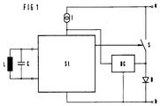
- Figure 1 shows an inductive two-wire proximity switch.
- a first connection a can be connected to the one pole of a voltage source and a second connection b can be connected to the one connection of a load, the other connection of the load then being connected to the other pole of the voltage source.
- the voltage source thus supplies a control circuit St. via a power supply circuit I.
- the control circuit St is externally connected to a parallel resonant circuit composed of a coil L and a capacitor C.
- the resonant circuit is damped and the control circuit St emits a signal from its output Q, possibly via an amplifier, to the electronic switching element S, whereupon the latter is closed.
- a current then flows through the electronic switching element S, the diode D, which is connected in series for this purpose which causes a voltage drop that is largely independent of the level of the load current and the connected but not shown load.
- the voltage now falling across the electronic switching element S and the diode D would not be sufficient to supply the control circuit St via the power supply circuit I further.
- a self-oscillating DC-DC converter DC is arranged in such a way that it is acted upon on the input side by the voltage drop across the diode and is connected on the output side to the control circuit St and supplies it with a sufficient voltage.
- FIG. 2 now shows a detailed circuit diagram of an inductive two-wire proximity switch according to the invention.
- the parallel resonant circuit consisting of the coil L and the capacitor C is connected between the connections 1 and 7 of the control circuit St, which can be provided, for example, by the integrated module TCA 505B from Siemens.
- the connection 2 of the control circuit St is connected via a resistor R1, with which the switching distance can be set, to the second connection b of the proximity switch, which is the same as the ground connection.
- a resistor R2 can be connected between the connections 2 and 5 to set the switching hysteresis, which is indicated by the broken line.
- the connections 4, 13 and 15 are each connected to the ground connection 7 via capacitors C2, C3 and C4.
- the power supply circuit I connected to the supply connection 12 of the control circuit St is formed in a manner known per se with a self-conducting field effect transistor T1 and a resistor R3 and a diode D1 connected in series with the field effect transistor T1.
- a self-conducting field effect transistor T1 and a resistor R3 and a diode D1 connected in series with the field effect transistor T1.
- the two outputs Q, Q ⁇ are designed as open collector outputs and the emitter of the output transistor of output Q is connected to ground and the emitter of the output transistor of the output Q ⁇ is not connected.
- the output Q of the control circuit St controls, via an amplifier V, the control connection of the electronic switching element formed with a logic-level MOSFET T2, ie with a logic-level-responsive MOSFET.
- the amplifier V is formed with a transistor T5 operated in an emitter circuit, a base resistor R5 and a collector resistor R4, a capacitor C8 also being connected in parallel to the collector-emitter path of the transistor T5, and the amplifier V being supplied by the power supply circuit I. .
- Two transistors T3, T4 and a resistor R6 connected as diodes are connected in series with the MOSFET T2. Together with the MOSFET T2, they form the switching path of the proximity switch.
- the voltage across the resistor R6 is fed to a terminal 6 of the control circuit St for overcurrent detection.
- the voltage drop across the two diodes T3 and T4 and across the resistor R6 form the input voltage for a DC-DC converter DC, the output of which is also connected to the supply connection 12 of the control circuit St.
- a Zener diode D4 is also connected in parallel to the output of the DC-DC converter DC.
- the circuit diagram according to FIG. 2 shows a first exemplary embodiment of a DC-DC converter DC according to the invention with a step-up converter.
- the step-up converter is formed by the primary winding W1 of a transformer Tr, a transistor T6, a first diode D2 and a first capacitor C5, the voltage on the first capacitor C5 being equal to a first output voltage of the circuit arrangement.
- the base of the transistor T6 is connected to the connection point of a serial RC element, which is formed with a first resistor R7 and a second capacitor C6 and is arranged in parallel with the input of the DC-DC converter, via a second resistor R8 and a first secondary winding W2 of the transformer Tr connected.
- a third capacitor is located parallel to the input of the DC-DC converter DC C7 switched as a buffer capacitor.
- a light-emitting diode D3 and a resistor R9 connected in series therewith are arranged parallel to the collector-emitter path of the transistor T6.
- This circuit arrangement already oscillates at an input voltage which corresponds to the base-emitter threshold of the transistor T6. It works self-regulating within certain limits, i. That is, excess energy at the input is not necessarily pumped through the converter, so that there is a constant first output voltage within certain limits.
- the first output voltage can be selected at an input voltage of approximately 0.7 volts to 2 volts to 4 volts to 6 volts, so that the control circuit St for the inductive two-wire proximity switch can thus be supplied.
- the DC-DC converter DC formed with a step-up converter according to the circuit arrangement according to FIG. 2 can also be used as an electronic switching element in a two-wire proximity switch with a bipolar transistor or a Darlington configuration made of bipolar transistors.
- Figure 3 shows such a two-wire proximity switch.
- the electronic switching element is provided by the bipolar transistor T9, to the base of which the input of the DC-DC converter DC is connected.
- the amplifier V ' is in this case connected to an npn transistor T5, the collector of which is connected via a resistor R4 to the connection a of the proximity switch and to the base connection of a pnp transistor T8, the emitter of which is also connected to the connection a via a resistor R10 connected is.
- the base of the NPN transistor T5 is connected to the output 10 of the control circuit St via a resistor R5 and to ground via a resistor R12.
- the emitter of the NPN transistor T5 is connected to ground via a resistor R11.
- the collector of the pnp transistor T8 is connected to the base of the transistor T9 forming the electronic switching element.
- the output 11 of the control circuit St is connected to the current source I.
- the circuits of an inductive two-wire proximity switch shown in FIGS. 2 and 3 are suitable for driving an electronic switch formed by a logic level MOSFET T2 or a bipolar transistor T9.
- a power MOSFET or an IGBT switching element is selected as the electronic switching element, a higher voltage at its control input is necessary for safe switching through than can be generated by the amplifier V or V '.
- a sufficiently high voltage is generated by the circuit shown in FIG. 4.
- the transistor T2 shown there is a power MOSFET or an IGBT switching element.
- FIG. 4 the same parts as have already been explained in FIG. 2 are provided with the same reference symbols.
- the DC-DC converter DC 'in FIG. 4 is expanded compared to the DC-DC converter DC in FIG. 2 by a second secondary winding W3, one end of which connects to the first output of the DC-DC converter DC' and the second end of which a second diode D5 is connected to a second output of the DC-DC converter DC ', the winding sense of the second secondary winding W3 being opposite to that of the primary winding W1.
- the second output of the DC-DC converter DC ' is connected to the control terminal of the transistor T2 via a resistor R10.
- the buffer capacitor of this second output circuit, designed as a flyback converter, of the DC-DC converter DC ' is formed on the one hand by the output capacitor C8 of the amplifier V and on the other hand by the gate capacitance of the MOSFET T2.
- the self-oscillating DC-DC converter according to the invention can of course be used not only used in the inductive two-wire proximity switches shown there, but also in every two-wire on-off switch, in which, when the electronic switching element used is switched on, a small residual voltage is designed to supply a DC-DC converter that is not designed to operate a clocked DC-DC converter Control circuit must be sufficient.
Landscapes
- Electronic Switches (AREA)
Abstract
Claims (8)
- Interrupteur marche-arrêt à deux fils, contenant :- un circuit de commande (St) qui peut être commandé de l'extérieur et qui est relié à une première borne (a) pour la connexion à une source de tension par le biais d'un circuit d'alimentation en courant électrique (l), et à une seconde borne (b) pour la connexion à une charge également reliée à la source de tension,- un élément de commutation électronique (S, T2, T9) pouvant être commandé par le circuit de commande (St) et qui est relié à la première borne (a) et par le biais d'un élément (D, T3, T4, R6) produisant une chute de tension, à la seconde borne (b), et- un convertisseur à courant continu (DC, DC') contenant un élément inductif et commandé par impulsions, qui est relié, côté entrée, au point de jonction formé entre l'élément de commutation (S, T2, T9) et l'élément (D, T3, T4, R6) produisant la chute de tension et, côté sortie, au circuit de commande (St) en vue de l'alimentation en tension de ce dernier, caractérisé en ce que le convertisseur à courant continu est prévu avec un montage en série formé par l'enroulement primaire (W1) d'un transformateur (Tr) et le circuit collecteur-émetteur d'un transistor (T6), qui est disposé en parallèle à l'élément (D, T3, T4, R6) produisant la chute de tension et formant une source de tension d'entrée; avec un montage en série formé par une première diode (D2) et un premier condensateur (C5) qui est disposé en parallèle au circuit collecteur-émetteur du transistor (T6), la tension aux bornes du premier condensateur (C5) alimentant le circuit de commande en tant que première tension de sortie du convertisseur à courant continu; et avec un montage en série formé par une première résistance (R7) et un second condensateur (C6) qui sont disposés en parallèle à la source de tension d'entrée (D, T3, T4, R6), la base du transistor (T6) étant reliée, par le biais d'une seconde résistance (R8) et d'un enroulement secondaire (W2) du transformateur (Tr) dont le sens d'enroulement est contraire à celui de l'enroulement primaire (W1), au point de jonction de la première résistance (R7) et du second condensateur (C6).
- Interrupteur marche-arrêt à deux fils selon la revendication 1, caractérisé en ce qu'un troisième condensateur (C7) est monté en parallèle à la source de tension d'entrée (T2, T4, R6).
- Interrupteur marche-arrêt à deux fils selon l'une des revendications 1 ou 2, caractérisé en ce qu'un montage en série qui est formé par un autre enroulement secondaire (W3) du transformateur (Tr) dont le sens d'enroulement est contraire à celui de l'enroulement primaire (W1), par une seconde diode (D5) et un quatrième condensateur (C8), est monté en parallèle au premier condensateur (C5), la tension aux bornes du quatrième condensateur (C8) étant une deuxième tension de sortie du convertisseur à courant continu (DC').
- Interrupteur marche-arrêt à deux fils selon la revendication 1 ou 2, caractérisé en ce que l'élément de commutation électronique (S) est un transistor MOS (T2) à niveau logique.
- Interrupteur marche-arrêt à deux fils selon la revendication 3, caractérisé en ce que l'élément de commutation électronique (S) est un transistor MOS de puissance ou un transistor IGBT dont l'entrée de commande reçoit, en plus, la deuxième tension de sortie du convertisseur à courant continu (DC').
- Interrupteur marche-arrêt à deux fils selon l'une des revendications 1 ou 2, caractérisé en ce que l'élément de commutation électronique (S) est un transistor bipolaire (T9) ou un montage Darlington de transistors bipolaires.
- Interrupteur marche-arrêt à deux fils selon la revendication 6, caractérisé en ce que l'entrée du convertisseur à courant continu (DC) est reliée à la base du transistor bipolaire (T9).
- Interrupteur marche-arrêt à deux fils selon l'une des revendications 1 à 5, caractérisé en ce que l'élément de commutation électronique (S; T2; T9) est commandé par le circuit de commande (St) par le biais d'un étage amplificateur (V; V').
Applications Claiming Priority (3)
| Application Number | Priority Date | Filing Date | Title |
|---|---|---|---|
| DE4310910 | 1993-04-02 | ||
| DE4310910A DE4310910C2 (de) | 1993-04-02 | 1993-04-02 | Zweidraht-Ein-Aus-Schalter |
| PCT/DE1994/000126 WO1994023499A1 (fr) | 1993-04-02 | 1994-02-08 | Interrupteur marche-arret a deux fils |
Publications (2)
| Publication Number | Publication Date |
|---|---|
| EP0692159A1 EP0692159A1 (fr) | 1996-01-17 |
| EP0692159B1 true EP0692159B1 (fr) | 1997-09-10 |
Family
ID=6484624
Family Applications (1)
| Application Number | Title | Priority Date | Filing Date |
|---|---|---|---|
| EP94906847A Revoked EP0692159B1 (fr) | 1993-04-02 | 1994-02-08 | Interrupteur marche-arret a deux fils |
Country Status (3)
| Country | Link |
|---|---|
| EP (1) | EP0692159B1 (fr) |
| DE (2) | DE4310910C2 (fr) |
| WO (1) | WO1994023499A1 (fr) |
Families Citing this family (2)
| Publication number | Priority date | Publication date | Assignee | Title |
|---|---|---|---|---|
| DE19501232C1 (de) * | 1995-01-17 | 1996-06-05 | Erich Dipl Ing Dickfeld | Verfahren und Schaltungsanordnung für einen kapazitiven, digitalen Annäherungsschalter |
| DE19517936C1 (de) * | 1995-05-18 | 1996-07-25 | Ifm Electronic Gmbh | Elektronisches, vorzugsweise berührungslos arbeitendes Schaltgerät |
Citations (1)
| Publication number | Priority date | Publication date | Assignee | Title |
|---|---|---|---|---|
| EP0019813A1 (fr) * | 1979-05-31 | 1980-12-10 | Siemens Aktiengesellschaft | Commutateur électronique marche-arrêt à effleurement |
Family Cites Families (7)
| Publication number | Priority date | Publication date | Assignee | Title |
|---|---|---|---|---|
| CH1251571A4 (fr) * | 1971-08-26 | 1975-03-14 | ||
| US3764880A (en) * | 1972-05-08 | 1973-10-09 | Rosemount Inc | Two-wire current transmitter with isolated transducer circuit |
| US4015472A (en) * | 1976-03-09 | 1977-04-05 | Fischer & Porter Co. | Two-wire transmission system for vortex flowmeter |
| US4242665A (en) * | 1978-09-15 | 1980-12-30 | Action Instruments Company, Inc. | Two-wire transmitter |
| JPS55141970A (en) * | 1979-04-21 | 1980-11-06 | Yoshiyuki Takematsu | Power supply device |
| DE3320975C2 (de) * | 1983-06-10 | 1987-02-19 | Ifm Electronic Gmbh, 4300 Essen | Elektronisches, vorzugsweise berührungslos arbeitendes Schaltgerät |
| DE4233488C1 (de) * | 1992-10-05 | 1993-12-23 | Ifm Electronic Gmbh | Schaltungsanordnung zur Überwachung eines Schaltgerätes und der an ihm angeschlossenen Außenleiter |
-
1993
- 1993-04-02 DE DE4310910A patent/DE4310910C2/de not_active Expired - Fee Related
-
1994
- 1994-02-08 DE DE59404038T patent/DE59404038D1/de not_active Revoked
- 1994-02-08 EP EP94906847A patent/EP0692159B1/fr not_active Revoked
- 1994-02-08 WO PCT/DE1994/000126 patent/WO1994023499A1/fr not_active Ceased
Patent Citations (1)
| Publication number | Priority date | Publication date | Assignee | Title |
|---|---|---|---|---|
| EP0019813A1 (fr) * | 1979-05-31 | 1980-12-10 | Siemens Aktiengesellschaft | Commutateur électronique marche-arrêt à effleurement |
Also Published As
| Publication number | Publication date |
|---|---|
| DE59404038D1 (de) | 1997-10-16 |
| DE4310910C2 (de) | 1995-06-14 |
| EP0692159A1 (fr) | 1996-01-17 |
| WO1994023499A1 (fr) | 1994-10-13 |
| DE4310910A1 (de) | 1994-10-06 |
Similar Documents
| Publication | Publication Date | Title |
|---|---|---|
| DE69224833T2 (de) | Leistungs-mosfet-treiber mit reduzierung des querstroms | |
| EP0498917B1 (fr) | Convertisseur commandé par horloge avec limitation de courant | |
| DE69604996T2 (de) | Halbbrückentreiberschaltung | |
| DE68924394T2 (de) | Vorrichtung zum Erzeugen einer Referenzspannung für einen eine kapazitive Bootstrapschaltung enthaltenden Schalter. | |
| DE3126525C2 (de) | "Spannungsgesteuerter Halbleiterschalter und damit versehene Spannungswandlerschaltung" | |
| DE69530077T2 (de) | Startschaltung, MOS Transistor mit solch einer Schaltung | |
| DE4125510A1 (de) | Schaltungsanordnung mit einem schaltnetzteil | |
| EP0639308A1 (fr) | Circuit pour commander un transistor a effet de champ mos. | |
| DE10252827B3 (de) | Schaltungsanordnung zur schnellen Ansteuerung insbesondere induktiver Lasten | |
| EP1783910B1 (fr) | Circuit et un procédé pour commander d'une manière galvaniquement séparée un commutateur semi-conducteur | |
| EP0794619A2 (fr) | Montage pour le commande d'un transistor à effet de champ à charge connectée à la source | |
| EP0131146A1 (fr) | Appareil de commutation électronique, fonctionnant de préférence sans contact | |
| DE69226004T2 (de) | Bootstrapschaltung zum Treiben von einem Leistungs-MOS-Transistor in einem Erhöhungsmode | |
| DE19736894C2 (de) | Integrierte Treiberschaltung | |
| DE69206484T2 (de) | Gleichstrom-Niederspannungswandler. | |
| EP0201878A2 (fr) | Circuit à transistor MOS à canal N commutant un potentiel positif | |
| EP0590304A2 (fr) | Procédé pour la commande pilote d'une alimentation en courant commutée pour légalisation de la tension d'alimentation | |
| DE4310910C2 (de) | Zweidraht-Ein-Aus-Schalter | |
| EP0560086B1 (fr) | Circuit de protection pour un transistor à effet de champ MOS de puissance attaquant une charge inductive | |
| DE3137940C2 (de) | Elektronisches Vorschaltgerät für mindestens eine Leuchtstofflampe | |
| DE10064123A1 (de) | Schaltungsanordnung zur Ansteuerung eines Halbleiterschaltelements | |
| DE3600170C2 (fr) | ||
| EP0581091B1 (fr) | Ballast pour alimenter des lampes à décharge haute-pression avec un signal carré basse-fréquence dans des véhicules | |
| DE69808043T2 (de) | Gerät und Verfahren zum Zünden und Betreiben einer Leuchtstofflampe | |
| DE69120228T2 (de) | Treiberschaltung |
Legal Events
| Date | Code | Title | Description |
|---|---|---|---|
| PUAI | Public reference made under article 153(3) epc to a published international application that has entered the european phase |
Free format text: ORIGINAL CODE: 0009012 |
|
| 17P | Request for examination filed |
Effective date: 19950927 |
|
| AK | Designated contracting states |
Kind code of ref document: A1 Designated state(s): CH DE FR GB IT LI |
|
| 17Q | First examination report despatched |
Effective date: 19960605 |
|
| GRAG | Despatch of communication of intention to grant |
Free format text: ORIGINAL CODE: EPIDOS AGRA |
|
| GRAH | Despatch of communication of intention to grant a patent |
Free format text: ORIGINAL CODE: EPIDOS IGRA |
|
| GRAH | Despatch of communication of intention to grant a patent |
Free format text: ORIGINAL CODE: EPIDOS IGRA |
|
| GRAA | (expected) grant |
Free format text: ORIGINAL CODE: 0009210 |
|
| AK | Designated contracting states |
Kind code of ref document: B1 Designated state(s): CH DE FR GB IT LI |
|
| REG | Reference to a national code |
Ref country code: CH Ref legal event code: NV Representative=s name: SIEMENS SCHWEIZ AG Ref country code: CH Ref legal event code: EP |
|
| REF | Corresponds to: |
Ref document number: 59404038 Country of ref document: DE Date of ref document: 19971016 |
|
| ET | Fr: translation filed | ||
| ITF | It: translation for a ep patent filed | ||
| GBT | Gb: translation of ep patent filed (gb section 77(6)(a)/1977) |
Effective date: 19971113 |
|
| PGFP | Annual fee paid to national office [announced via postgrant information from national office to epo] |
Ref country code: CH Payment date: 19980515 Year of fee payment: 5 |
|
| PLBQ | Unpublished change to opponent data |
Free format text: ORIGINAL CODE: EPIDOS OPPO |
|
| PLBI | Opposition filed |
Free format text: ORIGINAL CODE: 0009260 |
|
| PLBF | Reply of patent proprietor to notice(s) of opposition |
Free format text: ORIGINAL CODE: EPIDOS OBSO |
|
| 26 | Opposition filed |
Opponent name: WERNER TURCK GMBH & CO.KG Effective date: 19980609 |
|
| PLBF | Reply of patent proprietor to notice(s) of opposition |
Free format text: ORIGINAL CODE: EPIDOS OBSO |
|
| PLBF | Reply of patent proprietor to notice(s) of opposition |
Free format text: ORIGINAL CODE: EPIDOS OBSO |
|
| PG25 | Lapsed in a contracting state [announced via postgrant information from national office to epo] |
Ref country code: LI Free format text: LAPSE BECAUSE OF NON-PAYMENT OF DUE FEES Effective date: 19990228 Ref country code: CH Free format text: LAPSE BECAUSE OF NON-PAYMENT OF DUE FEES Effective date: 19990228 |
|
| REG | Reference to a national code |
Ref country code: CH Ref legal event code: PL |
|
| PGFP | Annual fee paid to national office [announced via postgrant information from national office to epo] |
Ref country code: GB Payment date: 20010208 Year of fee payment: 8 |
|
| PGFP | Annual fee paid to national office [announced via postgrant information from national office to epo] |
Ref country code: FR Payment date: 20010223 Year of fee payment: 8 |
|
| PGFP | Annual fee paid to national office [announced via postgrant information from national office to epo] |
Ref country code: DE Payment date: 20010419 Year of fee payment: 8 |
|
| REG | Reference to a national code |
Ref country code: GB Ref legal event code: IF02 |
|
| RDAH | Patent revoked |
Free format text: ORIGINAL CODE: EPIDOS REVO |
|
| RDAH | Patent revoked |
Free format text: ORIGINAL CODE: EPIDOS REVO |
|
| RDAG | Patent revoked |
Free format text: ORIGINAL CODE: 0009271 |
|
| STAA | Information on the status of an ep patent application or granted ep patent |
Free format text: STATUS: PATENT REVOKED |
|
| 27W | Patent revoked |
Effective date: 20020204 |
|
| GBPR | Gb: patent revoked under art. 102 of the ep convention designating the uk as contracting state |
Free format text: 20020204 |