EP0694801A2 - Amélioration concernant les dispositifs micromécaniques - Google Patents
Amélioration concernant les dispositifs micromécaniques Download PDFInfo
- Publication number
- EP0694801A2 EP0694801A2 EP95111689A EP95111689A EP0694801A2 EP 0694801 A2 EP0694801 A2 EP 0694801A2 EP 95111689 A EP95111689 A EP 95111689A EP 95111689 A EP95111689 A EP 95111689A EP 0694801 A2 EP0694801 A2 EP 0694801A2
- Authority
- EP
- European Patent Office
- Prior art keywords
- support post
- depositing
- layer
- micro
- mirror
- Prior art date
- Legal status (The legal status is an assumption and is not a legal conclusion. Google has not performed a legal analysis and makes no representation as to the accuracy of the status listed.)
- Granted
Links
Images



Classifications
-
- G—PHYSICS
- G02—OPTICS
- G02B—OPTICAL ELEMENTS, SYSTEMS OR APPARATUS
- G02B26/00—Optical devices or arrangements for the control of light using movable or deformable optical elements
- G02B26/08—Optical devices or arrangements for the control of light using movable or deformable optical elements for controlling the direction of light
- G02B26/0816—Optical devices or arrangements for the control of light using movable or deformable optical elements for controlling the direction of light by means of one or more reflecting elements
- G02B26/0833—Optical devices or arrangements for the control of light using movable or deformable optical elements for controlling the direction of light by means of one or more reflecting elements the reflecting element being a micromechanical device, e.g. a MEMS mirror, DMD
- G02B26/0841—Optical devices or arrangements for the control of light using movable or deformable optical elements for controlling the direction of light by means of one or more reflecting elements the reflecting element being a micromechanical device, e.g. a MEMS mirror, DMD the reflecting element being moved or deformed by electrostatic means
-
- H—ELECTRICITY
- H10—SEMICONDUCTOR DEVICES; ELECTRIC SOLID-STATE DEVICES NOT OTHERWISE PROVIDED FOR
- H10P—GENERIC PROCESSES OR APPARATUS FOR THE MANUFACTURE OR TREATMENT OF DEVICES COVERED BY CLASS H10
- H10P95/00—Generic processes or apparatus for manufacture or treatments not covered by the other groups of this subclass
-
- Y—GENERAL TAGGING OF NEW TECHNOLOGICAL DEVELOPMENTS; GENERAL TAGGING OF CROSS-SECTIONAL TECHNOLOGIES SPANNING OVER SEVERAL SECTIONS OF THE IPC; TECHNICAL SUBJECTS COVERED BY FORMER USPC CROSS-REFERENCE ART COLLECTIONS [XRACs] AND DIGESTS
- Y10—TECHNICAL SUBJECTS COVERED BY FORMER USPC
- Y10S—TECHNICAL SUBJECTS COVERED BY FORMER USPC CROSS-REFERENCE ART COLLECTIONS [XRACs] AND DIGESTS
- Y10S359/00—Optical: systems and elements
- Y10S359/90—Methods
Definitions
- This invention relates to micro-mechanical devices, and more particularly, to an improved method of fabricating support posts for their movable elements.
- micro-mechanical devices are manufactured using integrated circuit techniques, often together with electrical control circuitry.
- Common applications include accelerometers, pressure sensors, and actuators.
- spatial light modulators can be configured from micro-mechanical pixels.
- micro-mechanical spatial light modulator is a digital micro-mirror device (DMD), sometimes referred to as a deformable mirror device.
- DMD digital micro-mirror device
- the DMD has an array of hundreds or thousands of tiny tilting mirrors. Light incident on the DMD is selectively reflected or not reflected from each mirror to an image plane, to form images. To permit the mirrors to tilt, each is attached to one or more binges mounted on support posts, and spaced by means of an air gap over underlying control circuitry.
- the control circuitry provides electrostatic forces, which cause each mirror to selectively tilt.
- DMDs have various designs, most of which include the fabrication of support posts to which the binges are attached. Fabrication of the support posts has been accomplished with various approaches. One approach is to etch vias in a layer of spacer material. Metal is then deposited into the vias to coat each via's inner surface, resulting in a hollow metal post. A problem with this method is that it is difficult to uniformly coat the via's inner surface. In the terminology of silicon processing, good “step coverage" of the depositing material is difficult to achieve, and the coating inside the vias will typically have aberrations where the layer is very thin. Poor step coverage is an increasing problem as the aspect ratio of the vias increases. As a result, the support posts are mechanically weak.
- a method of fabricating a support post for a micro-mechanical device comprising depositing a spacer layer over a substrate; etching a via into said spacer layer, the via defining an outer surface of a support post; depositing an oxide layer over the spacer layer and into the via, such that said oxide layer substantially conformally coats an inside surface of the via; etching back said oxide layer to a level substantially corresponding to a top surface of the spacer layer, such that a sidewall ring remaining from said oxide layer coats the inside surface of the via; depositing a post metal layer over the spacer layer, such that the post metal layer coats the inside surface of the sidewall ring; and etching the post metal layer to form the support post.
- the deposition of the oxide layer is performed at a temperature in the range between room temperature (14°) and 120°C, and it is particularly preferred that the deposition is performed at room temperature.
- the deposition of the oxide layer is performed by means of a flourotinetuoxysilane or a tetramethyl silane (TMDS) source.
- TMDS tetramethyl silane
- the step of etching back the oxide layer is preferably performed with an anisotropic etch.
- the deposition of the post metal layer is performed by sputtering.
- Another aspect of the invention is an improved micro-mechanical device of a type having support posts.
- the improvement is a support post having a support post stem, made from a stem material deposited into a via etched into a spacer layer that is subsequently removed.
- a sidewall ring surrounds the circumference of the stem, covering at least a portion of the inner surface or outer surface of the stem. The sidewall ring is made by depositing an oxide layer over the spacer layer and into the vias, then etching back the oxide layer to the top surface of the spacer layer.
- the sidewall ring is made before deposition of the stem material.
- This provides the via with an inner profile that is rounded at the top edge of the via, slightly convex, and having an angle greater than 90 degrees at the bottom. This profile greatly enhances the step coverage of the subsequently applied metal layer that will form the support post stem.
- the support-post is used for supporting a micro-mechanical element.
- the micro-mechanical element is a Digital Mirror Device (DMD).
- DMD Digital Mirror Device
- the micro-mechanical device comprises a substrate upon which at least one address electrode is fabricated, together with the support posts, a hinge extending from the support post, and a mirror attached to the binge which is deformable. Since the hinge is deformable the mirror may be tilted upon application of an external force.
- An advantage of the invention is that it provides a stronger support post.
- the sidewall rings improve the step coverage of the metal layer, in the sense that the thickness of the metal deposited on the inner surface of the vias is more uniform than with prior methods.
- the sidewall rings remain in place alter fabrication, so as to bolster the strength of the metal walls.
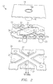
- FIGS 1 and 2 illustrate a digital micro-mirror device (DMD), made in accordance with the invention.
- DMD digital micro-mirror device
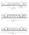
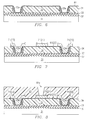
- FIGS. 3 - 12 illustrate the steps of the method of the invention.
- FIG. 13 illustrates an alternative embodiment of the invention.
- Figure 14 illustrates a second alternative embodiment of the invention.
- DMD digital micro-mirror device
- the DMD has an array of deflectable mirrors that selectively reflect light to an image plane.
- the images formed by the DMD can be used in display systems or for non-impact printing applications.
- Other applications of DMDs are possible that do not involve image formation, such as optical steering, optical switching, and accelerometers.
- the "mirror” need not be reflective and the applied force is due to acceleration rather than being electrostatic.
- the DMD is not necessarily operated in a digital mode.
- DMD is used herein to include any type of micro-mechanical device having at least one hinged and deflectable mass that is spaced by an air gap from a substrate, which it contacts in response to an applied force.
- the invention is used during fabrication of the DMD to provide support posts for the binges, and in some DMD designs, for other elements that are spaced above the substrate.
- Figure 1 is a plan view of a portion of a DMD 10 having an array of mirror elements 12. In the view of Figure 1, only the mirror 14 and mirror support post 16 of each mirror element 12 are shown. In a typical DMD 10, the mirror elements 12 are fabricated on 17 micron centers.
- FIG. 2 is an exploded perspective view of a single mirror element 12.
- the DMD 10 is a hidden-hinge type DMD.
- the hinges 22 are supported on support posts 23.
- address electrodes 24 are supported by electrode posts 25 on the same level as hinges 22 and binge support posts 23.
- the mirrors 14 are fabricated above the binge/electrode layer and are supported by mirror support posts 16.
- Mirror support post 16 is fabricated over a landing yoke 21.
- Landing yoke 21 is attached to one end of each of two torsion hinges 22.
- the other end of each torsion hinge 22 is attached to a hinge support post 23.
- Address electrodes 24 are supported by electrode support posts 25.
- the hinge support posts 23 and electrode support posts 25 support the hinges 22, address electrodes 24, and landing yoke 21 over a control bus 26 and address pads 27.
- the control bus 26 and landing pads 27 have appropriate electrical contacts with a substrate of address and control circuitry, which is typically fabricated within the substrate using CMOS fabrication techniques.
- each binge support post 23 is essentially a hollow stem 23b, made by depositing material into a via that has been etched in a spacer layer.
- a sidewall ring 23a coats the inner surface of each stem 23b. The spacer layer is subsequently removed, leaving the stem 23b and the sidewall ring 23a.
- the address electrode support posts 25a and mirror support posts 16a may be made in the same way.
- DMD for which the invention is useful is the torsion beam type, whose hinges are not hidden but rather extend from opposing sides of the mirror.
- Other types of DMDs are cantilever beam types and flexure beam types.
- Various DMD types are described in U.S. Patent No.4,662,746, entitled “Spatial Light Modulator and Method”; U.S. Patent No. 4,956,610, entitled “Spatial Light Modulator”; U.S. Patent No. 5,061,049 entitled “Spatial Light Modulator and Method”; U.S. Patent No. 5,083,857 entitled “Multi-level Deformable Mirror Device”; and U.S. Patent Serial No. 08/171,303, entitled “Improved Multi-Level Digital Micromirror Device”. Each of these patents is assigned to Texas Instruments Incorporated and each is incorporated herein by reference.
- a light source illuminates the surface of the DMD 10.
- a lens system may be used to shape the light to approximately the size of the array of mirror elements 12 and to direct this light toward them.
- the mirror support post 16 permits mirror 14 to rotate under control of hinge 22.
- Mirror 14 rotates in response to an electrostatic force caused by application of an appropriate voltage to an address electrode 24.
- yoke 21 contacts bus 26.
- Voltages based on data in the memory cells of the underlying CMOS circuit are applied to the two address electrodes 24, which are located under opposing comers of mirror 14. Electrostatic forces between the mirrors 14 and their address electrodes 24 are produced by selective application of voltages to the address electrodes 24. The electrostatic force causes each mirror 14 to tilt either about +10 degrees (on) or about -10 degrees (off), thereby modulating the light incident on the surface of the DMD. Light reflected from the "on” mirrors 14 is directed to an image plane, via display optics. Light from the "off” mirrors 14 is reflected away from the image plane. The resulting pattern forms an image. The proportion of time during each image frame that a mirror 14 is "on” determines shades of grey. Color can be added by means of a color wheel or by a three-DMD setup.
- the mirror 14 and its address electrodes 24 form capacitors.
- a resulting electrostatic force causes the mirror 14 to tilt toward the attracting address electrode 24 or away from the repelling address electrode 24.
- the mirror 14 tilts until yoke 21 contacts bus 26.
- the energy stored in the binge 22 provides a restoring force to return the mirror 14 to an undeflected position.
- Appropriate voltages may be applied to the mirror 14 or address electrodes 24 to aid in returning the mirror 14 to its undeflected position.
- Figures 3 - 12 illustrate the method aspects of the invention, which may be used to form any of the support posts 16, 23, or 25, for mirrors 14, hinges 22, or address electrodes 24, respectively.
- the method of the invention is described in terms of fabricating mirror elements 12 of a hidden-binge DMD 10 of the type described above. Except for the fabrication of support posts 16, 23, and 25, further details of fabrication of a DMD of this type are set out in U.S. Patent Serial No. 08/171,303 referred to above. With appropriate modifications, the method could be performed for fabrication of other types of DMDs, or for other types of micro-mechanical devices having support posts.
- CMOS substrate 31 This circuitry is shown as CMOS substrate 31.
- Substrate 31 is covered with a protective oxide layer 32.
- a metal layer 33 is then deposited, from which control bus 26 and landing address pads 27 are patterned and etched.
- holes are opened in the oxide layer 32 to permit the metal of layer 33 to contact the CMOS substrate 31.
- a hinge spacer layer 34 is then deposited, yielding a planar surface upon which to fabricate yoke 21 and hinges 22.
- the spacer layer 34 is patterned and etched to form vias 34a, which define the hinge support posts 23.
- vias 34a are round and define substantially cylindrical support posts 23, but other shapes could equivalently be used.
- vias for the address electrode support posts 24 are not visible, but could be made with the same method as described herein to make binge support posts 23.
- the thickness of layer 34 determines the size of the air gap under landing yoke 21, which in turn, determines the rotation angle of mirror 14.
- a typical spacer layer 34 is approximately 20,000 angstroms thick and is comprised of positive photoresist that is UV hardened.
- a layer 41 of sidewall oxide has been deposited over layer 34 and into vias 34a.
- Layer 41 is as conformal as possible.
- a typical thickness of layer 41 is 3000 angstroms.
- a suitable deposition technique involves the use of a fluorotriethoxysilane liquid source at room temperature. This source is described in an article entitled “Fluorinated Interlayer Dielectric Films in ULSI Multilevel Interconnections", by Tetsuya Homma, for E-MRS Spring Meeting 1994, Symposium A: Amorphous Insulating Thin Films II.
- TMDS tetramethyl siloxane
- a post metal layer 61 has been deposited over spacer layer 34 and into vias 34a.
- Layer 61 is referred to as a "post" metal layer although it may be used to form other elements, and in the example of this description, is used to form hinges 22 as well as hinge support posts 23. In particular, layer 61 forms the stem 23b of post 23.
- Layer 61 is approximately 600 angstroms thick.
- a typical material for post metal layer 61 is an aluminum alloy.
- a typical deposition means is sputtering.
- the deposition of layer 61 results in more uniform step coverage than would have occurred if the deposition were into via 34a without sidewall ring 23a.
- the thickness of the deposited layer near the top of via 34a is nearly the same as the thickness on the top surface of spacer layer 34.
- the inner profile of the support post 23, now defined by sidewall ring 23a and stem 23b corresponds to the profile of the via with sidewall ring 23a as discussed above.
- the profile is rounded at the top, slightly convex, and greater than 90 degrees at the bottom.
- Figure 7 illustrates the results of the etching steps for hinges 22 and yoke 21.
- a second metal layer 71 has been deposited over layer 61.
- Layer 71 is typically about 3000 angstroms thick.
- a typical material is an aluminum alloy.
- a plasma etch is used to pattern the hinges 22, electrodes 24 (not shown in Figure 7), tops of support posts 23, and yoke 21.
- oxide layers act as etch stops and protect the metal beneath them. After completion of the plasma etch, the oxide etch stops are removed.
- a mirror spacer layer 81 has been deposited over yoke 21, hinges 22, and electrodes 24 and patterned with vias 81a that define mirror support posts 16.
- a typical thickness of spacer layer 81 is 2.2 micrometers. It is UV hardened at a temperature of approximately 180 degrees centigrade.
- a sidewall ring 16a for mirror support post 16 has been formed around via 81a.
- This sidewall ring 16a is formed in a manner similar to that described above for the sidewall ring 23a for the hinge support posts 23. More specifically, an oxide layer 91 is conformally deposited and etched back.
- a mirror layer 111 has been deposited and patterned to form mirrors 14 and mirror support posts 16.
- a typical thickness of this layer 111 is 4250 angstroms.
- a typical material for layer 111 is an aluminum alloy.
- a masking oxide layer is deposited, then patterned, and etched with layer 111. This layer is left in place while the wafer is coated with a protective coating, sawed into chip arrays, and cleaned.
- Figure 13 illustrates an alternative to the above-described method, in which hinge metal layer 61 is deposited before the sidewall oxide layer 41. Otherwise, the sidewall rings 23a are fabricated in the same manner. The subsequent processing is the same as shown in Figures 6 - 12.
- An advantage of this alternative is that the metal layer 61 protects the sidewall rings 23a during removal of the spacer layer 34. The sidewall rings 23a remain in place to support the stem 23b of support post 23.
- Figure 14 illustrates a further alternative to the above described method, in which two metal layers 61a and 61b are deposited.
- One is deposited under sidewall layer 41 as in Figure 13.
- the other is deposited sidewall ring 23a as in Figure 6.
- Either or both layers 61a or 61b may be used to form hinges 22 and yoke 21.
Landscapes
- Physics & Mathematics (AREA)
- General Physics & Mathematics (AREA)
- Optics & Photonics (AREA)
- Mechanical Light Control Or Optical Switches (AREA)
- Micromachines (AREA)
- Optical Elements Other Than Lenses (AREA)
Applications Claiming Priority (2)
| Application Number | Priority Date | Filing Date | Title |
|---|---|---|---|
| US283486 | 1994-07-29 | ||
| US08/283,486 US5485304A (en) | 1994-07-29 | 1994-07-29 | Support posts for micro-mechanical devices |
Publications (3)
| Publication Number | Publication Date |
|---|---|
| EP0694801A2 true EP0694801A2 (fr) | 1996-01-31 |
| EP0694801A3 EP0694801A3 (fr) | 1996-04-24 |
| EP0694801B1 EP0694801B1 (fr) | 1999-03-10 |
Family
ID=23086290
Family Applications (1)
| Application Number | Title | Priority Date | Filing Date |
|---|---|---|---|
| EP95111689A Expired - Lifetime EP0694801B1 (fr) | 1994-07-29 | 1995-07-25 | Amélioration concernant les dispositifs micromécaniques |
Country Status (5)
| Country | Link |
|---|---|
| US (3) | US5485304A (fr) |
| EP (1) | EP0694801B1 (fr) |
| JP (1) | JP3790285B2 (fr) |
| KR (1) | KR100413014B1 (fr) |
| DE (1) | DE69508160T2 (fr) |
Cited By (3)
| Publication number | Priority date | Publication date | Assignee | Title |
|---|---|---|---|---|
| EP0877272A1 (fr) * | 1997-05-08 | 1998-11-11 | Texas Instruments Incorporated | Améliorations concernant les modulateurs de lumière spatiaux |
| WO2006036542A1 (fr) * | 2004-09-27 | 2006-04-06 | Idc, Llc | Modulateur optique interferometrique utilisant un materiau de remplissage et son procede de fabrication |
| US8830557B2 (en) | 2007-05-11 | 2014-09-09 | Qualcomm Mems Technologies, Inc. | Methods of fabricating MEMS with spacers between plates and devices formed by same |
Families Citing this family (323)
| Publication number | Priority date | Publication date | Assignee | Title |
|---|---|---|---|---|
| US6219015B1 (en) | 1992-04-28 | 2001-04-17 | The Board Of Directors Of The Leland Stanford, Junior University | Method and apparatus for using an array of grating light valves to produce multicolor optical images |
| US6674562B1 (en) * | 1994-05-05 | 2004-01-06 | Iridigm Display Corporation | Interferometric modulation of radiation |
| US6044705A (en) * | 1993-10-18 | 2000-04-04 | Xros, Inc. | Micromachined members coupled for relative rotation by torsion bars |
| US6467345B1 (en) | 1993-10-18 | 2002-10-22 | Xros, Inc. | Method of operating micromachined members coupled for relative rotation |
| US6426013B1 (en) | 1993-10-18 | 2002-07-30 | Xros, Inc. | Method for fabricating micromachined members coupled for relative rotation |
| US20030199179A1 (en) * | 1993-11-16 | 2003-10-23 | Formfactor, Inc. | Contact tip structure for microelectronic interconnection elements and method of making same |
| US7073254B2 (en) * | 1993-11-16 | 2006-07-11 | Formfactor, Inc. | Method for mounting a plurality of spring contact elements |
| US20020053734A1 (en) * | 1993-11-16 | 2002-05-09 | Formfactor, Inc. | Probe card assembly and kit, and methods of making same |
| US7550794B2 (en) * | 2002-09-20 | 2009-06-23 | Idc, Llc | Micromechanical systems device comprising a displaceable electrode and a charge-trapping layer |
| US6680792B2 (en) | 1994-05-05 | 2004-01-20 | Iridigm Display Corporation | Interferometric modulation of radiation |
| US7808694B2 (en) * | 1994-05-05 | 2010-10-05 | Qualcomm Mems Technologies, Inc. | Method and device for modulating light |
| US7138984B1 (en) | 2001-06-05 | 2006-11-21 | Idc, Llc | Directly laminated touch sensitive screen |
| US7123216B1 (en) | 1994-05-05 | 2006-10-17 | Idc, Llc | Photonic MEMS and structures |
| US7852545B2 (en) | 1994-05-05 | 2010-12-14 | Qualcomm Mems Technologies, Inc. | Method and device for modulating light |
| US7460291B2 (en) * | 1994-05-05 | 2008-12-02 | Idc, Llc | Separable modulator |
| US8014059B2 (en) | 1994-05-05 | 2011-09-06 | Qualcomm Mems Technologies, Inc. | System and method for charge control in a MEMS device |
| US7776631B2 (en) * | 1994-05-05 | 2010-08-17 | Qualcomm Mems Technologies, Inc. | MEMS device and method of forming a MEMS device |
| US7297471B1 (en) * | 2003-04-15 | 2007-11-20 | Idc, Llc | Method for manufacturing an array of interferometric modulators |
| KR100209401B1 (ko) * | 1994-07-21 | 1999-07-15 | 전주범 | 광로조절장치의 제조방법 |
| US5703728A (en) * | 1994-11-02 | 1997-12-30 | Texas Instruments Incorporated | Support post architecture for micromechanical devices |
| US5650881A (en) * | 1994-11-02 | 1997-07-22 | Texas Instruments Incorporated | Support post architecture for micromechanical devices |
| US7898722B2 (en) | 1995-05-01 | 2011-03-01 | Qualcomm Mems Technologies, Inc. | Microelectromechanical device with restoring electrode |
| US5841579A (en) | 1995-06-07 | 1998-11-24 | Silicon Light Machines | Flat diffraction grating light valve |
| KR100213026B1 (ko) * | 1995-07-27 | 1999-08-02 | 윤종용 | 디엠디 및 그 제조공정 |
| US5757536A (en) * | 1995-08-30 | 1998-05-26 | Sandia Corporation | Electrically-programmable diffraction grating |
| US5907425A (en) * | 1995-12-19 | 1999-05-25 | The Board Of Trustees Of The Leland Stanford Junior University | Miniature scanning confocal microscope |
| US8033838B2 (en) * | 1996-02-21 | 2011-10-11 | Formfactor, Inc. | Microelectronic contact structure |
| US7929197B2 (en) * | 1996-11-05 | 2011-04-19 | Qualcomm Mems Technologies, Inc. | System and method for a MEMS device |
| US7471444B2 (en) | 1996-12-19 | 2008-12-30 | Idc, Llc | Interferometric modulation of radiation |
| US7830588B2 (en) * | 1996-12-19 | 2010-11-09 | Qualcomm Mems Technologies, Inc. | Method of making a light modulating display device and associated transistor circuitry and structures thereof |
| US6028689A (en) * | 1997-01-24 | 2000-02-22 | The United States Of America As Represented By The Secretary Of The Air Force | Multi-motion micromirror |
| US5851302A (en) * | 1997-02-19 | 1998-12-22 | Vlsi Technology, Inc. | Method for dry etching sidewall polymer |
| US5925577A (en) * | 1997-02-19 | 1999-07-20 | Vlsi Technology, Inc. | Method for forming via contact hole in a semiconductor device |
| US5982553A (en) | 1997-03-20 | 1999-11-09 | Silicon Light Machines | Display device incorporating one-dimensional grating light-valve array |
| US6088102A (en) | 1997-10-31 | 2000-07-11 | Silicon Light Machines | Display apparatus including grating light-valve array and interferometric optical system |
| US7532377B2 (en) | 1998-04-08 | 2009-05-12 | Idc, Llc | Movable micro-electromechanical device |
| WO1999052006A2 (fr) | 1998-04-08 | 1999-10-14 | Etalon, Inc. | Modulation interferometrique de rayonnement |
| US8928967B2 (en) | 1998-04-08 | 2015-01-06 | Qualcomm Mems Technologies, Inc. | Method and device for modulating light |
| US6271808B1 (en) | 1998-06-05 | 2001-08-07 | Silicon Light Machines | Stereo head mounted display using a single display device |
| US6101036A (en) | 1998-06-23 | 2000-08-08 | Silicon Light Machines | Embossed diffraction grating alone and in combination with changeable image display |
| US6130770A (en) | 1998-06-23 | 2000-10-10 | Silicon Light Machines | Electron gun activated grating light valve |
| US6215579B1 (en) | 1998-06-24 | 2001-04-10 | Silicon Light Machines | Method and apparatus for modulating an incident light beam for forming a two-dimensional image |
| US6872984B1 (en) | 1998-07-29 | 2005-03-29 | Silicon Light Machines Corporation | Method of sealing a hermetic lid to a semiconductor die at an angle |
| US6303986B1 (en) | 1998-07-29 | 2001-10-16 | Silicon Light Machines | Method of and apparatus for sealing an hermetic lid to a semiconductor die |
| US6850353B1 (en) | 1999-06-11 | 2005-02-01 | University Of Hawaii | MEMS optical components |
| US6859299B1 (en) | 1999-06-11 | 2005-02-22 | Jung-Chih Chiao | MEMS optical components |
| AU5480500A (en) * | 1999-06-11 | 2001-01-02 | University Of Hawaii | Mems optical components |
| US6220561B1 (en) * | 1999-06-30 | 2001-04-24 | Sandia Corporation | Compound floating pivot micromechanisms |
| US6198180B1 (en) * | 1999-06-30 | 2001-03-06 | Sandia Corporation | Micromechanisms with floating pivot |
| WO2003007049A1 (fr) | 1999-10-05 | 2003-01-23 | Iridigm Display Corporation | Mems et structures photoniques |
| US6956878B1 (en) | 2000-02-07 | 2005-10-18 | Silicon Light Machines Corporation | Method and apparatus for reducing laser speckle using polarization averaging |
| US6813053B1 (en) * | 2000-05-19 | 2004-11-02 | The Regents Of The University Of California | Apparatus and method for controlled cantilever motion through torsional beams and a counterweight |
| EP1180848B1 (fr) * | 2000-08-09 | 2010-01-20 | STMicroelectronics S.r.l. | Structure microélectromécanique comprenant des parties distinctes reliées mécaniquement par un dispositif de conversion d'un mouvement de translation en un mouvement de rotation |
| US6522454B2 (en) * | 2000-09-29 | 2003-02-18 | Texas Instruments Incorporated | Hidden hinge digital micromirror device with improved manufacturing yield and improved contrast ratio |
| US6962771B1 (en) * | 2000-10-13 | 2005-11-08 | Taiwan Semiconductor Manufacturing Company, Ltd. | Dual damascene process |
| US6647164B1 (en) | 2000-10-31 | 2003-11-11 | 3M Innovative Properties Company | Gimbaled micro-mirror positionable by thermal actuators |
| US6711318B2 (en) | 2001-01-29 | 2004-03-23 | 3M Innovative Properties Company | Optical switch based on rotating vertical micro-mirror |
| FR2820833B1 (fr) * | 2001-02-15 | 2004-05-28 | Teem Photonics | Micro-miroir optique a pivot, matrice de tels micro-miroirs et procede de realisation dudit micro-miroir |
| FR2820834B1 (fr) * | 2001-02-15 | 2004-06-25 | Teem Photonics | Procede de fabrication d'un micro-miroir optique et micro-miroir ou matrice de micro-miroirs obtenu par ce procede |
| US6429033B1 (en) * | 2001-02-20 | 2002-08-06 | Nayna Networks, Inc. | Process for manufacturing mirror devices using semiconductor technology |
| US7177081B2 (en) | 2001-03-08 | 2007-02-13 | Silicon Light Machines Corporation | High contrast grating light valve type device |
| US6707591B2 (en) | 2001-04-10 | 2004-03-16 | Silicon Light Machines | Angled illumination for a single order light modulator based projection system |
| US6608712B2 (en) * | 2001-05-15 | 2003-08-19 | Network Photonics, Inc. | Hidden flexure ultra planar optical routing element |
| US7209274B2 (en) * | 2001-06-02 | 2007-04-24 | Capella Photonics, Inc. | High fill-factor bulk silicon mirrors |
| US6865346B1 (en) | 2001-06-05 | 2005-03-08 | Silicon Light Machines Corporation | Fiber optic transceiver |
| US6747781B2 (en) | 2001-06-25 | 2004-06-08 | Silicon Light Machines, Inc. | Method, apparatus, and diffuser for reducing laser speckle |
| US6782205B2 (en) | 2001-06-25 | 2004-08-24 | Silicon Light Machines | Method and apparatus for dynamic equalization in wavelength division multiplexing |
| US6589625B1 (en) | 2001-08-01 | 2003-07-08 | Iridigm Display Corporation | Hermetic seal and method to create the same |
| US6829092B2 (en) | 2001-08-15 | 2004-12-07 | Silicon Light Machines, Inc. | Blazed grating light valve |
| US6639722B2 (en) | 2001-08-15 | 2003-10-28 | Silicon Light Machines | Stress tuned blazed grating light valve |
| US6785001B2 (en) * | 2001-08-21 | 2004-08-31 | Silicon Light Machines, Inc. | Method and apparatus for measuring wavelength jitter of light signal |
| US6930364B2 (en) | 2001-09-13 | 2005-08-16 | Silicon Light Machines Corporation | Microelectronic mechanical system and methods |
| US6956995B1 (en) | 2001-11-09 | 2005-10-18 | Silicon Light Machines Corporation | Optical communication arrangement |
| US6800238B1 (en) | 2002-01-15 | 2004-10-05 | Silicon Light Machines, Inc. | Method for domain patterning in low coercive field ferroelectrics |
| US6794119B2 (en) | 2002-02-12 | 2004-09-21 | Iridigm Display Corporation | Method for fabricating a structure for a microelectromechanical systems (MEMS) device |
| US6574033B1 (en) | 2002-02-27 | 2003-06-03 | Iridigm Display Corporation | Microelectromechanical systems device and method for fabricating same |
| US6728023B1 (en) | 2002-05-28 | 2004-04-27 | Silicon Light Machines | Optical device arrays with optimized image resolution |
| KR100431581B1 (ko) * | 2002-05-28 | 2004-05-17 | 한국과학기술원 | 미소거울 구동기 |
| US6767751B2 (en) | 2002-05-28 | 2004-07-27 | Silicon Light Machines, Inc. | Integrated driver process flow |
| US7054515B1 (en) | 2002-05-30 | 2006-05-30 | Silicon Light Machines Corporation | Diffractive light modulator-based dynamic equalizer with integrated spectral monitor |
| US6822797B1 (en) | 2002-05-31 | 2004-11-23 | Silicon Light Machines, Inc. | Light modulator structure for producing high-contrast operation using zero-order light |
| US6829258B1 (en) | 2002-06-26 | 2004-12-07 | Silicon Light Machines, Inc. | Rapidly tunable external cavity laser |
| US6908201B2 (en) | 2002-06-28 | 2005-06-21 | Silicon Light Machines Corporation | Micro-support structures |
| US6813059B2 (en) | 2002-06-28 | 2004-11-02 | Silicon Light Machines, Inc. | Reduced formation of asperities in contact micro-structures |
| US6714337B1 (en) | 2002-06-28 | 2004-03-30 | Silicon Light Machines | Method and device for modulating a light beam and having an improved gamma response |
| US6801354B1 (en) | 2002-08-20 | 2004-10-05 | Silicon Light Machines, Inc. | 2-D diffraction grating for substantially eliminating polarization dependent losses |
| US7057795B2 (en) * | 2002-08-20 | 2006-06-06 | Silicon Light Machines Corporation | Micro-structures with individually addressable ribbon pairs |
| US7781850B2 (en) | 2002-09-20 | 2010-08-24 | Qualcomm Mems Technologies, Inc. | Controlling electromechanical behavior of structures within a microelectromechanical systems device |
| US6712480B1 (en) | 2002-09-27 | 2004-03-30 | Silicon Light Machines | Controlled curvature of stressed micro-structures |
| US6928207B1 (en) | 2002-12-12 | 2005-08-09 | Silicon Light Machines Corporation | Apparatus for selectively blocking WDM channels |
| US6987600B1 (en) | 2002-12-17 | 2006-01-17 | Silicon Light Machines Corporation | Arbitrary phase profile for better equalization in dynamic gain equalizer |
| US7057819B1 (en) | 2002-12-17 | 2006-06-06 | Silicon Light Machines Corporation | High contrast tilting ribbon blazed grating |
| US6934070B1 (en) | 2002-12-18 | 2005-08-23 | Silicon Light Machines Corporation | Chirped optical MEM device |
| US6927891B1 (en) | 2002-12-23 | 2005-08-09 | Silicon Light Machines Corporation | Tilt-able grating plane for improved crosstalk in 1×N blaze switches |
| US7068372B1 (en) | 2003-01-28 | 2006-06-27 | Silicon Light Machines Corporation | MEMS interferometer-based reconfigurable optical add-and-drop multiplexor |
| TW200413810A (en) | 2003-01-29 | 2004-08-01 | Prime View Int Co Ltd | Light interference display panel and its manufacturing method |
| US7286764B1 (en) | 2003-02-03 | 2007-10-23 | Silicon Light Machines Corporation | Reconfigurable modulator-based optical add-and-drop multiplexer |
| US6947613B1 (en) | 2003-02-11 | 2005-09-20 | Silicon Light Machines Corporation | Wavelength selective switch and equalizer |
| US6922272B1 (en) | 2003-02-14 | 2005-07-26 | Silicon Light Machines Corporation | Method and apparatus for leveling thermal stress variations in multi-layer MEMS devices |
| US7391973B1 (en) | 2003-02-28 | 2008-06-24 | Silicon Light Machines Corporation | Two-stage gain equalizer |
| US6829077B1 (en) | 2003-02-28 | 2004-12-07 | Silicon Light Machines, Inc. | Diffractive light modulator with dynamically rotatable diffraction plane |
| US6922273B1 (en) | 2003-02-28 | 2005-07-26 | Silicon Light Machines Corporation | PDL mitigation structure for diffractive MEMS and gratings |
| US7027202B1 (en) | 2003-02-28 | 2006-04-11 | Silicon Light Machines Corp | Silicon substrate as a light modulator sacrificial layer |
| US6806997B1 (en) | 2003-02-28 | 2004-10-19 | Silicon Light Machines, Inc. | Patterned diffractive light modulator ribbon for PDL reduction |
| US7042611B1 (en) | 2003-03-03 | 2006-05-09 | Silicon Light Machines Corporation | Pre-deflected bias ribbons |
| TW594360B (en) | 2003-04-21 | 2004-06-21 | Prime View Int Corp Ltd | A method for fabricating an interference display cell |
| TW570896B (en) | 2003-05-26 | 2004-01-11 | Prime View Int Co Ltd | A method for fabricating an interference display cell |
| TWI223855B (en) * | 2003-06-09 | 2004-11-11 | Taiwan Semiconductor Mfg | Method for manufacturing reflective spatial light modulator mirror devices |
| US7221495B2 (en) * | 2003-06-24 | 2007-05-22 | Idc Llc | Thin film precursor stack for MEMS manufacturing |
| TWI231865B (en) | 2003-08-26 | 2005-05-01 | Prime View Int Co Ltd | An interference display cell and fabrication method thereof |
| TW593126B (en) * | 2003-09-30 | 2004-06-21 | Prime View Int Co Ltd | A structure of a micro electro mechanical system and manufacturing the same |
| US6914709B2 (en) * | 2003-10-02 | 2005-07-05 | Hewlett-Packard Development Company, L.P. | MEMS device and method of forming MEMS device |
| US6861277B1 (en) | 2003-10-02 | 2005-03-01 | Hewlett-Packard Development Company, L.P. | Method of forming MEMS device |
| US7352053B2 (en) * | 2003-10-29 | 2008-04-01 | Taiwan Semiconductor Manufacturing Company, Ltd. | Insulating layer having decreased dielectric constant and increased hardness |
| US7876488B2 (en) | 2003-11-01 | 2011-01-25 | Silicon Quest Kabushiki-Kaisha | Mirror device having vertical hinge |
| US7755830B2 (en) * | 2003-11-01 | 2010-07-13 | Silicon Quest Kabushiki-Kaisha | Micro mirror device |
| US7933060B2 (en) * | 2003-11-01 | 2011-04-26 | Silicon Quest Kabushiki-Kaisha | Three states of micro mirror device |
| US7760415B2 (en) * | 2003-11-01 | 2010-07-20 | Silicon Quest Kabushiki-Kaisha | Micro mirror device |
| US7643195B2 (en) * | 2003-11-01 | 2010-01-05 | Silicon Quest Kabushiki-Kaisha | Mirror device |
| US7012726B1 (en) | 2003-11-03 | 2006-03-14 | Idc, Llc | MEMS devices with unreleased thin film components |
| US7142346B2 (en) | 2003-12-09 | 2006-11-28 | Idc, Llc | System and method for addressing a MEMS display |
| US7161728B2 (en) | 2003-12-09 | 2007-01-09 | Idc, Llc | Area array modulation and lead reduction in interferometric modulators |
| US7532194B2 (en) | 2004-02-03 | 2009-05-12 | Idc, Llc | Driver voltage adjuster |
| US7119945B2 (en) | 2004-03-03 | 2006-10-10 | Idc, Llc | Altering temporal response of microelectromechanical elements |
| US7706050B2 (en) | 2004-03-05 | 2010-04-27 | Qualcomm Mems Technologies, Inc. | Integrated modulator illumination |
| US7720148B2 (en) * | 2004-03-26 | 2010-05-18 | The Hong Kong University Of Science And Technology | Efficient multi-frame motion estimation for video compression |
| US7476327B2 (en) | 2004-05-04 | 2009-01-13 | Idc, Llc | Method of manufacture for microelectromechanical devices |
| US7060895B2 (en) | 2004-05-04 | 2006-06-13 | Idc, Llc | Modifying the electro-mechanical behavior of devices |
| US7164520B2 (en) | 2004-05-12 | 2007-01-16 | Idc, Llc | Packaging for an interferometric modulator |
| US7256922B2 (en) | 2004-07-02 | 2007-08-14 | Idc, Llc | Interferometric modulators with thin film transistors |
| US6974219B1 (en) * | 2004-07-09 | 2005-12-13 | Bae Systems Information And Electronic Systems Integration Inc | Zero reflectance design for tilted devices |
| WO2006014929A1 (fr) * | 2004-07-29 | 2006-02-09 | Idc, Llc | Systeme et procede pour le fonctionnement micro-electromecanique d'un modulateur interferometrique |
| US7408179B2 (en) * | 2004-08-10 | 2008-08-05 | Intel Corporation | Transition radiation apparatus and method therefor |
| US7515147B2 (en) | 2004-08-27 | 2009-04-07 | Idc, Llc | Staggered column drive circuit systems and methods |
| US7499208B2 (en) | 2004-08-27 | 2009-03-03 | Udc, Llc | Current mode display driver circuit realization feature |
| US7560299B2 (en) * | 2004-08-27 | 2009-07-14 | Idc, Llc | Systems and methods of actuating MEMS display elements |
| US7551159B2 (en) | 2004-08-27 | 2009-06-23 | Idc, Llc | System and method of sensing actuation and release voltages of an interferometric modulator |
| US7889163B2 (en) | 2004-08-27 | 2011-02-15 | Qualcomm Mems Technologies, Inc. | Drive method for MEMS devices |
| US7602375B2 (en) | 2004-09-27 | 2009-10-13 | Idc, Llc | Method and system for writing data to MEMS display elements |
| US20060076634A1 (en) | 2004-09-27 | 2006-04-13 | Lauren Palmateer | Method and system for packaging MEMS devices with incorporated getter |
| US7532195B2 (en) | 2004-09-27 | 2009-05-12 | Idc, Llc | Method and system for reducing power consumption in a display |
| US7545550B2 (en) | 2004-09-27 | 2009-06-09 | Idc, Llc | Systems and methods of actuating MEMS display elements |
| US7564612B2 (en) | 2004-09-27 | 2009-07-21 | Idc, Llc | Photonic MEMS and structures |
| US7372613B2 (en) | 2004-09-27 | 2008-05-13 | Idc, Llc | Method and device for multistate interferometric light modulation |
| US8124434B2 (en) | 2004-09-27 | 2012-02-28 | Qualcomm Mems Technologies, Inc. | Method and system for packaging a display |
| US7710629B2 (en) | 2004-09-27 | 2010-05-04 | Qualcomm Mems Technologies, Inc. | System and method for display device with reinforcing substance |
| US7936497B2 (en) | 2004-09-27 | 2011-05-03 | Qualcomm Mems Technologies, Inc. | MEMS device having deformable membrane characterized by mechanical persistence |
| US7161730B2 (en) | 2004-09-27 | 2007-01-09 | Idc, Llc | System and method for providing thermal compensation for an interferometric modulator display |
| CN100439967C (zh) * | 2004-09-27 | 2008-12-03 | Idc公司 | 用于多状态干涉光调制的方法和设备 |
| US7369294B2 (en) | 2004-09-27 | 2008-05-06 | Idc, Llc | Ornamental display device |
| US7343080B2 (en) | 2004-09-27 | 2008-03-11 | Idc, Llc | System and method of testing humidity in a sealed MEMS device |
| US7345805B2 (en) | 2004-09-27 | 2008-03-18 | Idc, Llc | Interferometric modulator array with integrated MEMS electrical switches |
| US7317568B2 (en) | 2004-09-27 | 2008-01-08 | Idc, Llc | System and method of implementation of interferometric modulators for display mirrors |
| US7373026B2 (en) | 2004-09-27 | 2008-05-13 | Idc, Llc | MEMS device fabricated on a pre-patterned substrate |
| US7289256B2 (en) | 2004-09-27 | 2007-10-30 | Idc, Llc | Electrical characterization of interferometric modulators |
| US7420725B2 (en) | 2004-09-27 | 2008-09-02 | Idc, Llc | Device having a conductive light absorbing mask and method for fabricating same |
| US7259449B2 (en) | 2004-09-27 | 2007-08-21 | Idc, Llc | Method and system for sealing a substrate |
| US7893919B2 (en) | 2004-09-27 | 2011-02-22 | Qualcomm Mems Technologies, Inc. | Display region architectures |
| US7136213B2 (en) | 2004-09-27 | 2006-11-14 | Idc, Llc | Interferometric modulators having charge persistence |
| US8514169B2 (en) | 2004-09-27 | 2013-08-20 | Qualcomm Mems Technologies, Inc. | Apparatus and system for writing data to electromechanical display elements |
| US7701631B2 (en) | 2004-09-27 | 2010-04-20 | Qualcomm Mems Technologies, Inc. | Device having patterned spacers for backplates and method of making the same |
| US7675669B2 (en) | 2004-09-27 | 2010-03-09 | Qualcomm Mems Technologies, Inc. | Method and system for driving interferometric modulators |
| US7668415B2 (en) | 2004-09-27 | 2010-02-23 | Qualcomm Mems Technologies, Inc. | Method and device for providing electronic circuitry on a backplate |
| US7535466B2 (en) | 2004-09-27 | 2009-05-19 | Idc, Llc | System with server based control of client device display features |
| US7692839B2 (en) | 2004-09-27 | 2010-04-06 | Qualcomm Mems Technologies, Inc. | System and method of providing MEMS device with anti-stiction coating |
| US7405861B2 (en) | 2004-09-27 | 2008-07-29 | Idc, Llc | Method and device for protecting interferometric modulators from electrostatic discharge |
| US7553684B2 (en) | 2004-09-27 | 2009-06-30 | Idc, Llc | Method of fabricating interferometric devices using lift-off processing techniques |
| US7630119B2 (en) | 2004-09-27 | 2009-12-08 | Qualcomm Mems Technologies, Inc. | Apparatus and method for reducing slippage between structures in an interferometric modulator |
| US7446927B2 (en) | 2004-09-27 | 2008-11-04 | Idc, Llc | MEMS switch with set and latch electrodes |
| US7299681B2 (en) | 2004-09-27 | 2007-11-27 | Idc, Llc | Method and system for detecting leak in electronic devices |
| US8310441B2 (en) | 2004-09-27 | 2012-11-13 | Qualcomm Mems Technologies, Inc. | Method and system for writing data to MEMS display elements |
| US7310179B2 (en) * | 2004-09-27 | 2007-12-18 | Idc, Llc | Method and device for selective adjustment of hysteresis window |
| US7527995B2 (en) | 2004-09-27 | 2009-05-05 | Qualcomm Mems Technologies, Inc. | Method of making prestructure for MEMS systems |
| US7417783B2 (en) | 2004-09-27 | 2008-08-26 | Idc, Llc | Mirror and mirror layer for optical modulator and method |
| US7369296B2 (en) | 2004-09-27 | 2008-05-06 | Idc, Llc | Device and method for modifying actuation voltage thresholds of a deformable membrane in an interferometric modulator |
| US7368803B2 (en) | 2004-09-27 | 2008-05-06 | Idc, Llc | System and method for protecting microelectromechanical systems array using back-plate with non-flat portion |
| US7808703B2 (en) | 2004-09-27 | 2010-10-05 | Qualcomm Mems Technologies, Inc. | System and method for implementation of interferometric modulator displays |
| US7944599B2 (en) | 2004-09-27 | 2011-05-17 | Qualcomm Mems Technologies, Inc. | Electromechanical device with optical function separated from mechanical and electrical function |
| US7492502B2 (en) | 2004-09-27 | 2009-02-17 | Idc, Llc | Method of fabricating a free-standing microstructure |
| US7415186B2 (en) | 2004-09-27 | 2008-08-19 | Idc, Llc | Methods for visually inspecting interferometric modulators for defects |
| US7424198B2 (en) | 2004-09-27 | 2008-09-09 | Idc, Llc | Method and device for packaging a substrate |
| US7724993B2 (en) | 2004-09-27 | 2010-05-25 | Qualcomm Mems Technologies, Inc. | MEMS switches with deforming membranes |
| US7130104B2 (en) | 2004-09-27 | 2006-10-31 | Idc, Llc | Methods and devices for inhibiting tilting of a mirror in an interferometric modulator |
| US7813026B2 (en) | 2004-09-27 | 2010-10-12 | Qualcomm Mems Technologies, Inc. | System and method of reducing color shift in a display |
| US7405924B2 (en) | 2004-09-27 | 2008-07-29 | Idc, Llc | System and method for protecting microelectromechanical systems array using structurally reinforced back-plate |
| US7920135B2 (en) | 2004-09-27 | 2011-04-05 | Qualcomm Mems Technologies, Inc. | Method and system for driving a bi-stable display |
| US7586484B2 (en) | 2004-09-27 | 2009-09-08 | Idc, Llc | Controller and driver features for bi-stable display |
| US7626581B2 (en) | 2004-09-27 | 2009-12-01 | Idc, Llc | Device and method for display memory using manipulation of mechanical response |
| US20060176487A1 (en) | 2004-09-27 | 2006-08-10 | William Cummings | Process control monitors for interferometric modulators |
| US7612932B2 (en) * | 2004-09-27 | 2009-11-03 | Idc, Llc | Microelectromechanical device with optical function separated from mechanical and electrical function |
| US7719500B2 (en) | 2004-09-27 | 2010-05-18 | Qualcomm Mems Technologies, Inc. | Reflective display pixels arranged in non-rectangular arrays |
| US7355780B2 (en) | 2004-09-27 | 2008-04-08 | Idc, Llc | System and method of illuminating interferometric modulators using backlighting |
| US7843410B2 (en) | 2004-09-27 | 2010-11-30 | Qualcomm Mems Technologies, Inc. | Method and device for electrically programmable display |
| US7349136B2 (en) | 2004-09-27 | 2008-03-25 | Idc, Llc | Method and device for a display having transparent components integrated therein |
| US7429334B2 (en) | 2004-09-27 | 2008-09-30 | Idc, Llc | Methods of fabricating interferometric modulators by selectively removing a material |
| US7289259B2 (en) | 2004-09-27 | 2007-10-30 | Idc, Llc | Conductive bus structure for interferometric modulator array |
| US7417735B2 (en) | 2004-09-27 | 2008-08-26 | Idc, Llc | Systems and methods for measuring color and contrast in specular reflective devices |
| US7679627B2 (en) | 2004-09-27 | 2010-03-16 | Qualcomm Mems Technologies, Inc. | Controller and driver features for bi-stable display |
| US7916103B2 (en) * | 2004-09-27 | 2011-03-29 | Qualcomm Mems Technologies, Inc. | System and method for display device with end-of-life phenomena |
| US8008736B2 (en) | 2004-09-27 | 2011-08-30 | Qualcomm Mems Technologies, Inc. | Analog interferometric modulator device |
| US7554714B2 (en) | 2004-09-27 | 2009-06-30 | Idc, Llc | Device and method for manipulation of thermal response in a modulator |
| US7321456B2 (en) | 2004-09-27 | 2008-01-22 | Idc, Llc | Method and device for corner interferometric modulation |
| US7327510B2 (en) | 2004-09-27 | 2008-02-05 | Idc, Llc | Process for modifying offset voltage characteristics of an interferometric modulator |
| US7359066B2 (en) | 2004-09-27 | 2008-04-15 | Idc, Llc | Electro-optical measurement of hysteresis in interferometric modulators |
| US7653371B2 (en) | 2004-09-27 | 2010-01-26 | Qualcomm Mems Technologies, Inc. | Selectable capacitance circuit |
| US7302157B2 (en) | 2004-09-27 | 2007-11-27 | Idc, Llc | System and method for multi-level brightness in interferometric modulation |
| US8878825B2 (en) | 2004-09-27 | 2014-11-04 | Qualcomm Mems Technologies, Inc. | System and method for providing a variable refresh rate of an interferometric modulator display |
| US7583429B2 (en) | 2004-09-27 | 2009-09-01 | Idc, Llc | Ornamental display device |
| US7460246B2 (en) | 2004-09-27 | 2008-12-02 | Idc, Llc | Method and system for sensing light using interferometric elements |
| US7304784B2 (en) | 2004-09-27 | 2007-12-04 | Idc, Llc | Reflective display device having viewable display on both sides |
| US7453579B2 (en) | 2004-09-27 | 2008-11-18 | Idc, Llc | Measurement of the dynamic characteristics of interferometric modulators |
| US7184193B2 (en) * | 2004-10-05 | 2007-02-27 | Hewlett-Packard Development Company, L.P. | Systems and methods for amorphous flexures in micro-electro mechanical systems |
| US20080186550A1 (en) * | 2005-01-17 | 2008-08-07 | Koninklijke Philips Electronics, N.V. | Micro Electromechanical Device For Tilting A Body In Two Degrees Of Freedom |
| TW200628877A (en) | 2005-02-04 | 2006-08-16 | Prime View Int Co Ltd | Method of manufacturing optical interference type color display |
| US7948457B2 (en) | 2005-05-05 | 2011-05-24 | Qualcomm Mems Technologies, Inc. | Systems and methods of actuating MEMS display elements |
| US7920136B2 (en) | 2005-05-05 | 2011-04-05 | Qualcomm Mems Technologies, Inc. | System and method of driving a MEMS display device |
| CA2607807A1 (fr) | 2005-05-05 | 2006-11-16 | Qualcomm Incorporated | Circuit integre pilote dynamique et configuration de panneau afficheur |
| US7884989B2 (en) | 2005-05-27 | 2011-02-08 | Qualcomm Mems Technologies, Inc. | White interferometric modulators and methods for forming the same |
| EP2495212A3 (fr) * | 2005-07-22 | 2012-10-31 | QUALCOMM MEMS Technologies, Inc. | Dispositifs MEMS comportant des structures de support et procédés de fabrication associés |
| JP2009503564A (ja) | 2005-07-22 | 2009-01-29 | クアルコム,インコーポレイテッド | Memsデバイスのための支持構造、およびその方法 |
| RU2468988C2 (ru) * | 2005-07-22 | 2012-12-10 | Квалкомм Инкорпорэйтэд | Устройства мэмс, имеющие поддерживающие структуры, и способы их изготовления |
| KR20080040715A (ko) * | 2005-07-22 | 2008-05-08 | 콸콤 인코포레이티드 | Mems 장치를 위한 지지 구조물 및 그 방법들 |
| US7355779B2 (en) | 2005-09-02 | 2008-04-08 | Idc, Llc | Method and system for driving MEMS display elements |
| US7630114B2 (en) | 2005-10-28 | 2009-12-08 | Idc, Llc | Diffusion barrier layer for MEMS devices |
| US7522330B2 (en) * | 2005-10-28 | 2009-04-21 | Miradia Inc. | High fill ratio silicon spatial light modulator |
| US7675670B2 (en) | 2005-10-28 | 2010-03-09 | Miradia Inc. | Fabrication of a high fill ratio silicon spatial light modulator |
| US8391630B2 (en) | 2005-12-22 | 2013-03-05 | Qualcomm Mems Technologies, Inc. | System and method for power reduction when decompressing video streams for interferometric modulator displays |
| US7795061B2 (en) | 2005-12-29 | 2010-09-14 | Qualcomm Mems Technologies, Inc. | Method of creating MEMS device cavities by a non-etching process |
| US7636151B2 (en) | 2006-01-06 | 2009-12-22 | Qualcomm Mems Technologies, Inc. | System and method for providing residual stress test structures |
| US7916980B2 (en) | 2006-01-13 | 2011-03-29 | Qualcomm Mems Technologies, Inc. | Interconnect structure for MEMS device |
| US7382515B2 (en) | 2006-01-18 | 2008-06-03 | Qualcomm Mems Technologies, Inc. | Silicon-rich silicon nitrides as etch stops in MEMS manufacture |
| US8194056B2 (en) | 2006-02-09 | 2012-06-05 | Qualcomm Mems Technologies Inc. | Method and system for writing data to MEMS display elements |
| US7582952B2 (en) | 2006-02-21 | 2009-09-01 | Qualcomm Mems Technologies, Inc. | Method for providing and removing discharging interconnect for chip-on-glass output leads and structures thereof |
| US7547568B2 (en) | 2006-02-22 | 2009-06-16 | Qualcomm Mems Technologies, Inc. | Electrical conditioning of MEMS device and insulating layer thereof |
| US7550810B2 (en) | 2006-02-23 | 2009-06-23 | Qualcomm Mems Technologies, Inc. | MEMS device having a layer movable at asymmetric rates |
| US20070205507A1 (en) * | 2006-03-01 | 2007-09-06 | Hui-Lin Chang | Carbon and nitrogen based cap materials for metal hard mask scheme |
| US7450295B2 (en) * | 2006-03-02 | 2008-11-11 | Qualcomm Mems Technologies, Inc. | Methods for producing MEMS with protective coatings using multi-component sacrificial layers |
| US7643203B2 (en) | 2006-04-10 | 2010-01-05 | Qualcomm Mems Technologies, Inc. | Interferometric optical display system with broadband characteristics |
| US7903047B2 (en) | 2006-04-17 | 2011-03-08 | Qualcomm Mems Technologies, Inc. | Mode indicator for interferometric modulator displays |
| US7417784B2 (en) | 2006-04-19 | 2008-08-26 | Qualcomm Mems Technologies, Inc. | Microelectromechanical device and method utilizing a porous surface |
| US7711239B2 (en) | 2006-04-19 | 2010-05-04 | Qualcomm Mems Technologies, Inc. | Microelectromechanical device and method utilizing nanoparticles |
| US7623287B2 (en) | 2006-04-19 | 2009-11-24 | Qualcomm Mems Technologies, Inc. | Non-planar surface structures and process for microelectromechanical systems |
| US7527996B2 (en) | 2006-04-19 | 2009-05-05 | Qualcomm Mems Technologies, Inc. | Non-planar surface structures and process for microelectromechanical systems |
| US8049713B2 (en) | 2006-04-24 | 2011-11-01 | Qualcomm Mems Technologies, Inc. | Power consumption optimized display update |
| US7761350B1 (en) * | 2006-04-26 | 2010-07-20 | Aol Inc. | Biasing of search result clustering to ensure more effective point of interest (POI) targeting |
| US7369292B2 (en) | 2006-05-03 | 2008-05-06 | Qualcomm Mems Technologies, Inc. | Electrode and interconnect materials for MEMS devices |
| US7321457B2 (en) | 2006-06-01 | 2008-01-22 | Qualcomm Incorporated | Process and structure for fabrication of MEMS device having isolated edge posts |
| US7649671B2 (en) | 2006-06-01 | 2010-01-19 | Qualcomm Mems Technologies, Inc. | Analog interferometric modulator device with electrostatic actuation and release |
| US7405863B2 (en) | 2006-06-01 | 2008-07-29 | Qualcomm Mems Technologies, Inc. | Patterning of mechanical layer in MEMS to reduce stresses at supports |
| US7471442B2 (en) | 2006-06-15 | 2008-12-30 | Qualcomm Mems Technologies, Inc. | Method and apparatus for low range bit depth enhancements for MEMS display architectures |
| US7702192B2 (en) | 2006-06-21 | 2010-04-20 | Qualcomm Mems Technologies, Inc. | Systems and methods for driving MEMS display |
| US7385744B2 (en) | 2006-06-28 | 2008-06-10 | Qualcomm Mems Technologies, Inc. | Support structure for free-standing MEMS device and methods for forming the same |
| US7835061B2 (en) | 2006-06-28 | 2010-11-16 | Qualcomm Mems Technologies, Inc. | Support structures for free-standing electromechanical devices |
| US7777715B2 (en) | 2006-06-29 | 2010-08-17 | Qualcomm Mems Technologies, Inc. | Passive circuits for de-multiplexing display inputs |
| US7527998B2 (en) | 2006-06-30 | 2009-05-05 | Qualcomm Mems Technologies, Inc. | Method of manufacturing MEMS devices providing air gap control |
| US7388704B2 (en) | 2006-06-30 | 2008-06-17 | Qualcomm Mems Technologies, Inc. | Determination of interferometric modulator mirror curvature and airgap variation using digital photographs |
| JP4327183B2 (ja) * | 2006-07-31 | 2009-09-09 | 株式会社日立製作所 | 内燃機関の高圧燃料ポンプ制御装置 |
| US7763546B2 (en) | 2006-08-02 | 2010-07-27 | Qualcomm Mems Technologies, Inc. | Methods for reducing surface charges during the manufacture of microelectromechanical systems devices |
| US7566664B2 (en) | 2006-08-02 | 2009-07-28 | Qualcomm Mems Technologies, Inc. | Selective etching of MEMS using gaseous halides and reactive co-etchants |
| KR100729117B1 (ko) | 2006-08-28 | 2007-06-14 | 동부일렉트로닉스 주식회사 | 디엘피 소자의 금속 배선 형성 방법 |
| US7652813B2 (en) * | 2006-08-30 | 2010-01-26 | Silicon Quest Kabushiki-Kaisha | Mirror device |
| US8023172B2 (en) * | 2006-08-30 | 2011-09-20 | Silicon Quest Kabushiki-Kaisha | Mirror device |
| US7629197B2 (en) | 2006-10-18 | 2009-12-08 | Qualcomm Mems Technologies, Inc. | Spatial light modulator |
| US7545552B2 (en) * | 2006-10-19 | 2009-06-09 | Qualcomm Mems Technologies, Inc. | Sacrificial spacer process and resultant structure for MEMS support structure |
| US7684106B2 (en) | 2006-11-02 | 2010-03-23 | Qualcomm Mems Technologies, Inc. | Compatible MEMS switch architecture |
| US20080180783A1 (en) * | 2007-01-25 | 2008-07-31 | Li-Ming Wang | Critical dimension control for photolithography for microelectromechanical systems devices |
| US8115987B2 (en) | 2007-02-01 | 2012-02-14 | Qualcomm Mems Technologies, Inc. | Modulating the intensity of light from an interferometric reflector |
| US7733552B2 (en) | 2007-03-21 | 2010-06-08 | Qualcomm Mems Technologies, Inc | MEMS cavity-coating layers and methods |
| US7742220B2 (en) | 2007-03-28 | 2010-06-22 | Qualcomm Mems Technologies, Inc. | Microelectromechanical device and method utilizing conducting layers separated by stops |
| US7715085B2 (en) * | 2007-05-09 | 2010-05-11 | Qualcomm Mems Technologies, Inc. | Electromechanical system having a dielectric movable membrane and a mirror |
| US7643202B2 (en) | 2007-05-09 | 2010-01-05 | Qualcomm Mems Technologies, Inc. | Microelectromechanical system having a dielectric movable membrane and a mirror |
| US7643199B2 (en) | 2007-06-19 | 2010-01-05 | Qualcomm Mems Technologies, Inc. | High aperture-ratio top-reflective AM-iMod displays |
| US7782517B2 (en) | 2007-06-21 | 2010-08-24 | Qualcomm Mems Technologies, Inc. | Infrared and dual mode displays |
| US7569488B2 (en) * | 2007-06-22 | 2009-08-04 | Qualcomm Mems Technologies, Inc. | Methods of making a MEMS device by monitoring a process parameter |
| US7630121B2 (en) | 2007-07-02 | 2009-12-08 | Qualcomm Mems Technologies, Inc. | Electromechanical device with optical function separated from mechanical and electrical function |
| US8068268B2 (en) | 2007-07-03 | 2011-11-29 | Qualcomm Mems Technologies, Inc. | MEMS devices having improved uniformity and methods for making them |
| US7813029B2 (en) | 2007-07-31 | 2010-10-12 | Qualcomm Mems Technologies, Inc. | Devices and methods for enhancing color shift of interferometric modulators |
| US8072402B2 (en) | 2007-08-29 | 2011-12-06 | Qualcomm Mems Technologies, Inc. | Interferometric optical modulator with broadband reflection characteristics |
| US7773286B2 (en) | 2007-09-14 | 2010-08-10 | Qualcomm Mems Technologies, Inc. | Periodic dimple array |
| US7847999B2 (en) | 2007-09-14 | 2010-12-07 | Qualcomm Mems Technologies, Inc. | Interferometric modulator display devices |
| KR20100090257A (ko) | 2007-10-19 | 2010-08-13 | 퀄컴 엠이엠스 테크놀로지스, 인크. | 광기전력 소자가 통합된 디스플레이 |
| US8058549B2 (en) | 2007-10-19 | 2011-11-15 | Qualcomm Mems Technologies, Inc. | Photovoltaic devices with integrated color interferometric film stacks |
| CN101836137A (zh) | 2007-10-23 | 2010-09-15 | 高通Mems科技公司 | 基于微机电系统的可调整透射装置 |
| US8941631B2 (en) | 2007-11-16 | 2015-01-27 | Qualcomm Mems Technologies, Inc. | Simultaneous light collection and illumination on an active display |
| US7820063B2 (en) * | 2007-11-16 | 2010-10-26 | Texas Instruments Incorporated | Micromirror device and a method of making the same |
| US7715079B2 (en) | 2007-12-07 | 2010-05-11 | Qualcomm Mems Technologies, Inc. | MEMS devices requiring no mechanical support |
| US8164821B2 (en) | 2008-02-22 | 2012-04-24 | Qualcomm Mems Technologies, Inc. | Microelectromechanical device with thermal expansion balancing layer or stiffening layer |
| US7944604B2 (en) | 2008-03-07 | 2011-05-17 | Qualcomm Mems Technologies, Inc. | Interferometric modulator in transmission mode |
| US7643305B2 (en) * | 2008-03-07 | 2010-01-05 | Qualcomm Mems Technologies, Inc. | System and method of preventing damage to metal traces of flexible printed circuits |
| US7612933B2 (en) | 2008-03-27 | 2009-11-03 | Qualcomm Mems Technologies, Inc. | Microelectromechanical device with spacing layer |
| US7898723B2 (en) | 2008-04-02 | 2011-03-01 | Qualcomm Mems Technologies, Inc. | Microelectromechanical systems display element with photovoltaic structure |
| US7969638B2 (en) | 2008-04-10 | 2011-06-28 | Qualcomm Mems Technologies, Inc. | Device having thin black mask and method of fabricating the same |
| US7851239B2 (en) * | 2008-06-05 | 2010-12-14 | Qualcomm Mems Technologies, Inc. | Low temperature amorphous silicon sacrificial layer for controlled adhesion in MEMS devices |
| US7768690B2 (en) | 2008-06-25 | 2010-08-03 | Qualcomm Mems Technologies, Inc. | Backlight displays |
| US8023167B2 (en) | 2008-06-25 | 2011-09-20 | Qualcomm Mems Technologies, Inc. | Backlight displays |
| US7746539B2 (en) | 2008-06-25 | 2010-06-29 | Qualcomm Mems Technologies, Inc. | Method for packing a display device and the device obtained thereof |
| US7859740B2 (en) | 2008-07-11 | 2010-12-28 | Qualcomm Mems Technologies, Inc. | Stiction mitigation with integrated mech micro-cantilevers through vertical stress gradient control |
| US7782522B2 (en) * | 2008-07-17 | 2010-08-24 | Qualcomm Mems Technologies, Inc. | Encapsulation methods for interferometric modulator and MEMS devices |
| US7855826B2 (en) | 2008-08-12 | 2010-12-21 | Qualcomm Mems Technologies, Inc. | Method and apparatus to reduce or eliminate stiction and image retention in interferometric modulator devices |
| US8358266B2 (en) | 2008-09-02 | 2013-01-22 | Qualcomm Mems Technologies, Inc. | Light turning device with prismatic light turning features |
| US8270056B2 (en) | 2009-03-23 | 2012-09-18 | Qualcomm Mems Technologies, Inc. | Display device with openings between sub-pixels and method of making same |
| US7864403B2 (en) | 2009-03-27 | 2011-01-04 | Qualcomm Mems Technologies, Inc. | Post-release adjustment of interferometric modulator reflectivity |
| US8736590B2 (en) * | 2009-03-27 | 2014-05-27 | Qualcomm Mems Technologies, Inc. | Low voltage driver scheme for interferometric modulators |
| WO2010138761A1 (fr) | 2009-05-29 | 2010-12-02 | Qualcomm Mems Technologies, Inc. | Dispositifs d'éclairage et leurs procédés de fabrication |
| US8270062B2 (en) | 2009-09-17 | 2012-09-18 | Qualcomm Mems Technologies, Inc. | Display device with at least one movable stop element |
| US8488228B2 (en) | 2009-09-28 | 2013-07-16 | Qualcomm Mems Technologies, Inc. | Interferometric display with interferometric reflector |
| US8547626B2 (en) * | 2010-03-25 | 2013-10-01 | Qualcomm Mems Technologies, Inc. | Mechanical layer and methods of shaping the same |
| US8368153B2 (en) * | 2010-04-08 | 2013-02-05 | United Microelectronics Corp. | Wafer level package of MEMS microphone and manufacturing method thereof |
| KR20130100232A (ko) | 2010-04-09 | 2013-09-10 | 퀄컴 엠이엠에스 테크놀로지스, 인크. | 전기 기계 디바이스의 기계층 및 그 형성 방법 |
| CN103109315A (zh) | 2010-08-17 | 2013-05-15 | 高通Mems科技公司 | 对干涉式显示装置中的电荷中性电极的激活和校准 |
| US9057872B2 (en) | 2010-08-31 | 2015-06-16 | Qualcomm Mems Technologies, Inc. | Dielectric enhanced mirror for IMOD display |
| US8963159B2 (en) | 2011-04-04 | 2015-02-24 | Qualcomm Mems Technologies, Inc. | Pixel via and methods of forming the same |
| US9134527B2 (en) | 2011-04-04 | 2015-09-15 | Qualcomm Mems Technologies, Inc. | Pixel via and methods of forming the same |
| US8659816B2 (en) | 2011-04-25 | 2014-02-25 | Qualcomm Mems Technologies, Inc. | Mechanical layer and methods of making the same |
| US20130100145A1 (en) * | 2011-10-21 | 2013-04-25 | Qualcomm Mems Technologies, Inc. | Electromechanical systems device |
| WO2013067023A1 (fr) * | 2011-10-31 | 2013-05-10 | The Charles Stark Draper Laboratory, Inc. | Gyroscope de résonateur hémisphérique de système micro-électromécanique (mems) |
| US8736939B2 (en) | 2011-11-04 | 2014-05-27 | Qualcomm Mems Technologies, Inc. | Matching layer thin-films for an electromechanical systems reflective display device |
| EP2618201B1 (fr) * | 2012-01-20 | 2015-11-04 | Imec | Étalonnage de réseaux de micromiroirs |
| WO2015080057A1 (fr) * | 2013-11-27 | 2015-06-04 | 株式会社ニコン | Modulateur spatial de lumière, appareil d'étirage de fibre optique, appareil d'exposition et procédé permettant de fabriquer un dispositif |
| US10916448B2 (en) | 2018-07-05 | 2021-02-09 | Texas Instruments Incorporated | Method for creating a wettable surface for improved reliability in QFN packages |
| US11131796B2 (en) | 2018-09-10 | 2021-09-28 | Texas Instruments Incorporated | Optical display with spatial light modulator |
| US12160084B2 (en) * | 2019-10-15 | 2024-12-03 | Texas Instruments Incorporated | MEMS-based phase spatial light modulating architecture |
| JP7842400B2 (ja) * | 2022-02-24 | 2026-04-08 | 新東工業株式会社 | 力覚センサの製造方法 |
Citations (4)
| Publication number | Priority date | Publication date | Assignee | Title |
|---|---|---|---|---|
| US4662746A (en) | 1985-10-30 | 1987-05-05 | Texas Instruments Incorporated | Spatial light modulator and method |
| US4956610A (en) | 1988-02-12 | 1990-09-11 | Pgm Diversified Industries, Inc. | Current density measurement system by self-sustaining magnetic oscillation |
| US5061049A (en) | 1984-08-31 | 1991-10-29 | Texas Instruments Incorporated | Spatial light modulator and method |
| US5083857A (en) | 1990-06-29 | 1992-01-28 | Texas Instruments Incorporated | Multi-level deformable mirror device |
Family Cites Families (9)
| Publication number | Priority date | Publication date | Assignee | Title |
|---|---|---|---|---|
| US4592628A (en) * | 1981-07-01 | 1986-06-03 | International Business Machines | Mirror array light valve |
| EP0139991A3 (fr) * | 1983-09-08 | 1986-06-25 | Texas Instruments Incorporated | Système optique pour l'affichage par projection utilisant un modulateur de lumière spatiale |
| US4638309A (en) * | 1983-09-08 | 1987-01-20 | Texas Instruments Incorporated | Spatial light modulator drive system |
| US4710732A (en) * | 1984-07-31 | 1987-12-01 | Texas Instruments Incorporated | Spatial light modulator and method |
| US4793699A (en) * | 1985-04-19 | 1988-12-27 | Canon Kabushiki Kaisha | Projection apparatus provided with an electro-mechanical transducer element |
| US5202785A (en) * | 1991-12-20 | 1993-04-13 | Texas Instruments Incorporated | Method and device for steering light |
| CA2085961A1 (fr) * | 1991-12-23 | 1993-06-24 | William E. Nelson | Methode et installation pour le braquage de sources lumineuses |
| US5289172A (en) * | 1992-10-23 | 1994-02-22 | Texas Instruments Incorporated | Method of mitigating the effects of a defective electromechanical pixel |
| KR100285696B1 (ko) * | 1992-12-16 | 2001-09-17 | 윌리엄 비. 켐플러 | 패터닝된 금속층의 세정방법 |
-
1994
- 1994-07-29 US US08/283,486 patent/US5485304A/en not_active Expired - Lifetime
-
1995
- 1995-06-07 US US08/476,959 patent/US5646768A/en not_active Expired - Lifetime
- 1995-06-07 US US08/476,961 patent/US5497262A/en not_active Expired - Lifetime
- 1995-07-25 EP EP95111689A patent/EP0694801B1/fr not_active Expired - Lifetime
- 1995-07-25 DE DE69508160T patent/DE69508160T2/de not_active Expired - Lifetime
- 1995-07-27 KR KR1019950022444A patent/KR100413014B1/ko not_active Expired - Lifetime
- 1995-07-28 JP JP19269095A patent/JP3790285B2/ja not_active Expired - Fee Related
Patent Citations (4)
| Publication number | Priority date | Publication date | Assignee | Title |
|---|---|---|---|---|
| US5061049A (en) | 1984-08-31 | 1991-10-29 | Texas Instruments Incorporated | Spatial light modulator and method |
| US4662746A (en) | 1985-10-30 | 1987-05-05 | Texas Instruments Incorporated | Spatial light modulator and method |
| US4956610A (en) | 1988-02-12 | 1990-09-11 | Pgm Diversified Industries, Inc. | Current density measurement system by self-sustaining magnetic oscillation |
| US5083857A (en) | 1990-06-29 | 1992-01-28 | Texas Instruments Incorporated | Multi-level deformable mirror device |
Cited By (3)
| Publication number | Priority date | Publication date | Assignee | Title |
|---|---|---|---|---|
| EP0877272A1 (fr) * | 1997-05-08 | 1998-11-11 | Texas Instruments Incorporated | Améliorations concernant les modulateurs de lumière spatiaux |
| WO2006036542A1 (fr) * | 2004-09-27 | 2006-04-06 | Idc, Llc | Modulateur optique interferometrique utilisant un materiau de remplissage et son procede de fabrication |
| US8830557B2 (en) | 2007-05-11 | 2014-09-09 | Qualcomm Mems Technologies, Inc. | Methods of fabricating MEMS with spacers between plates and devices formed by same |
Also Published As
| Publication number | Publication date |
|---|---|
| US5485304A (en) | 1996-01-16 |
| US5497262A (en) | 1996-03-05 |
| JP3790285B2 (ja) | 2006-06-28 |
| US5646768A (en) | 1997-07-08 |
| KR100413014B1 (ko) | 2004-03-25 |
| EP0694801A3 (fr) | 1996-04-24 |
| KR960005747A (ko) | 1996-02-23 |
| EP0694801B1 (fr) | 1999-03-10 |
| DE69508160T2 (de) | 1999-08-12 |
| JPH0862518A (ja) | 1996-03-08 |
| DE69508160D1 (de) | 1999-04-15 |
Similar Documents
| Publication | Publication Date | Title |
|---|---|---|
| EP0694801B1 (fr) | Amélioration concernant les dispositifs micromécaniques | |
| US5526951A (en) | Fabrication method for digital micro-mirror devices using low temperature CVD | |
| EP1315016B1 (fr) | Appareillage à micro-miroir numérique à charnière cachée sans bâti | |
| EP1704424B1 (fr) | Modulateur de lumiere spatial a fort contraste et procede associe | |
| US6856446B2 (en) | Digital micromirror device having mirror-attached spring tips | |
| US5665997A (en) | Grated landing area to eliminate sticking of micro-mechanical devices | |
| US6614576B2 (en) | Surface micro-planarization for enhanced optical efficiency and pixel performance in SLM devices | |
| US5454906A (en) | Method of providing sacrificial spacer for micro-mechanical devices | |
| US5652671A (en) | Hinge for micro-mechanical device | |
| US7471445B2 (en) | Fast-response micro-mechanical devices | |
| US7411713B2 (en) | Yokeless hidden hinge digital micromirror device with double binge layer | |
| KR100600248B1 (ko) | 디지털 마이크로 미러 및 그 제조방법 |
Legal Events
| Date | Code | Title | Description |
|---|---|---|---|
| PUAI | Public reference made under article 153(3) epc to a published international application that has entered the european phase |
Free format text: ORIGINAL CODE: 0009012 |
|
| AK | Designated contracting states |
Kind code of ref document: A2 Designated state(s): DE FR GB IT NL |
|
| PUAL | Search report despatched |
Free format text: ORIGINAL CODE: 0009013 |
|
| AK | Designated contracting states |
Kind code of ref document: A3 Designated state(s): DE FR GB IT NL |
|
| 17P | Request for examination filed |
Effective date: 19960729 |
|
| 17Q | First examination report despatched |
Effective date: 19960829 |
|
| GRAG | Despatch of communication of intention to grant |
Free format text: ORIGINAL CODE: EPIDOS AGRA |
|
| GRAG | Despatch of communication of intention to grant |
Free format text: ORIGINAL CODE: EPIDOS AGRA |
|
| GRAH | Despatch of communication of intention to grant a patent |
Free format text: ORIGINAL CODE: EPIDOS IGRA |
|
| GRAH | Despatch of communication of intention to grant a patent |
Free format text: ORIGINAL CODE: EPIDOS IGRA |
|
| GRAA | (expected) grant |
Free format text: ORIGINAL CODE: 0009210 |
|
| AK | Designated contracting states |
Kind code of ref document: B1 Designated state(s): DE FR GB IT NL |
|
| PG25 | Lapsed in a contracting state [announced via postgrant information from national office to epo] |
Ref country code: IT Free format text: LAPSE BECAUSE OF FAILURE TO SUBMIT A TRANSLATION OF THE DESCRIPTION OR TO PAY THE FEE WITHIN THE PRESCRIBED TIME-LIMIT;WARNING: LAPSES OF ITALIAN PATENTS WITH EFFECTIVE DATE BEFORE 2007 MAY HAVE OCCURRED AT ANY TIME BEFORE 2007. THE CORRECT EFFECTIVE DATE MAY BE DIFFERENT FROM THE ONE RECORDED. Effective date: 19990310 |
|
| REF | Corresponds to: |
Ref document number: 69508160 Country of ref document: DE Date of ref document: 19990415 |
|
| ET | Fr: translation filed | ||
| PLBE | No opposition filed within time limit |
Free format text: ORIGINAL CODE: 0009261 |
|
| STAA | Information on the status of an ep patent application or granted ep patent |
Free format text: STATUS: NO OPPOSITION FILED WITHIN TIME LIMIT |
|
| 26N | No opposition filed | ||
| REG | Reference to a national code |
Ref country code: GB Ref legal event code: IF02 |
|
| PGFP | Annual fee paid to national office [announced via postgrant information from national office to epo] |
Ref country code: FR Payment date: 20090708 Year of fee payment: 15 |
|
| PGFP | Annual fee paid to national office [announced via postgrant information from national office to epo] |
Ref country code: NL Payment date: 20090722 Year of fee payment: 15 |
|
| PGFP | Annual fee paid to national office [announced via postgrant information from national office to epo] |
Ref country code: GB Payment date: 20100616 Year of fee payment: 16 Ref country code: DE Payment date: 20100730 Year of fee payment: 16 |
|
| REG | Reference to a national code |
Ref country code: NL Ref legal event code: V1 Effective date: 20110201 |
|
| REG | Reference to a national code |
Ref country code: FR Ref legal event code: ST Effective date: 20110331 |
|
| PG25 | Lapsed in a contracting state [announced via postgrant information from national office to epo] |
Ref country code: FR Free format text: LAPSE BECAUSE OF NON-PAYMENT OF DUE FEES Effective date: 20100802 Ref country code: NL Free format text: LAPSE BECAUSE OF NON-PAYMENT OF DUE FEES Effective date: 20110201 |
|
| GBPC | Gb: european patent ceased through non-payment of renewal fee |
Effective date: 20110725 |
|
| PG25 | Lapsed in a contracting state [announced via postgrant information from national office to epo] |
Ref country code: DE Free format text: LAPSE BECAUSE OF NON-PAYMENT OF DUE FEES Effective date: 20120201 |
|
| REG | Reference to a national code |
Ref country code: DE Ref legal event code: R119 Ref document number: 69508160 Country of ref document: DE Effective date: 20120201 |
|
| PG25 | Lapsed in a contracting state [announced via postgrant information from national office to epo] |
Ref country code: GB Free format text: LAPSE BECAUSE OF NON-PAYMENT OF DUE FEES Effective date: 20110725 |