EP0694802B1 - Optischer Abtaster - Google Patents
Optischer Abtaster Download PDFInfo
- Publication number
- EP0694802B1 EP0694802B1 EP95111758A EP95111758A EP0694802B1 EP 0694802 B1 EP0694802 B1 EP 0694802B1 EP 95111758 A EP95111758 A EP 95111758A EP 95111758 A EP95111758 A EP 95111758A EP 0694802 B1 EP0694802 B1 EP 0694802B1
- Authority
- EP
- European Patent Office
- Prior art keywords
- scanning direction
- optical
- curved mirror
- image formation
- correction lens
- Prior art date
- Legal status (The legal status is an assumption and is not a legal conclusion. Google has not performed a legal analysis and makes no representation as to the accuracy of the status listed.)
- Expired - Lifetime
Links
Images


Classifications
-
- G—PHYSICS
- G02—OPTICS
- G02B—OPTICAL ELEMENTS, SYSTEMS OR APPARATUS
- G02B26/00—Optical devices or arrangements for the control of light using movable or deformable optical elements
- G02B26/08—Optical devices or arrangements for the control of light using movable or deformable optical elements for controlling the direction of light
- G02B26/10—Scanning systems
- G02B26/12—Scanning systems using multifaceted mirrors
- G02B26/125—Details of the optical system between the polygonal mirror and the image plane
- G02B26/126—Details of the optical system between the polygonal mirror and the image plane including curved mirrors
Definitions
- the present invention relates to an optical scanner used for laser beam printers, laser facsimiles, digital copying machines, and the like.
- optical scanner used for laser beam printers and the like include a semiconductor laser as a light source, a first image formation optical system for converging a light flux from the light source onto an optical deflector linearly for correcting a tilt of a deflection surface of the light deflector, a polygon mirror as the optical deflector, and a second image formation optical system for forming uniform spots on a surface to be scanned at a constant velocity.
- the second image formation optical system is conventionally composed of a plurality of large-size glass lenses called a f ⁇ lens.
- the f ⁇ lens is disadvantageous in that it is expensive and the size reduction thereof is difficult.
- optical scanners which use a cylindrical mirror and a cylindrical lens (Japanese Laid-Open Patent Publication No. 1-300218), a spherical mirror and a cylindrical lens (Japanese Laid-Open Patent Publication No. 1-300217), and an aspherical mirror and a long cylinder optical element (e.g., a long toric lens) (USP 5,408,095 or USP 5,173,798) for the second image formation optical system.
- the optical scanner of this invention includes a light source, an optical deflector for scanning a light flux from the light source, a first image formation optical system disposed between the light source and the optical deflector, and a second image formation optical system disposed between the optical deflector and a surface to be scanned, wherein the second image formation optical system includes a curved mirror for reflecting a light flux from the optical deflector and a correction lens for converging the light flux from the curved mirror on the surface to be scanned, a refractive power in a sub-scanning direction at a center of the correction lens in a scanning direction being different from a refractive power in a sub-scanning direction at a periphery of the correction lens, wherein, when a distance between a reflection point of the optical deflector and a reflection point of the curved mirror is L (mm), a distance between the reflection point of the curved mirror and an incident surface of the correction lens is M (mm), and the focal length of the second image formation optical system in the scanning
- an emergent surface of the correction lens is a cylindrical surface having a refractive power only in the scanning direction.
- an emergent surface of the correction lens is a aspherical cylindrical surface which has a refractive power only in the scanning direction and the section of the surface in the scanning direction has fourth or higher order development terms.
- the curved mirror has an axial-symmetric aspherical surface.
- conditional formula (2) when a displacement of a vertex of the curved mirror from an optical axis is x m (mm), conditional formula (2) below is satisfied: 0.5 ⁇ x m ⁇ 5.0
- an angle formed by a plane vertical to a reflection surface of the optical deflector and parallel to the scanning direction and an optical axis of the first image formation optical system is ⁇ P (deg.), a distance between a reflection point of the optical deflector and a reflection point of the curved mirror is L (mm), a distance between the reflection point of the curved mirror and the incident surface of the correction lens is M (mm), a focal length of the second image formation optical system in the scanning direction is f m (mm), and a displacement of a center of the incident surface of the correction lens from the optical axis in the sub-scanning direction is x L (mm), conditional formula (4) below is satisfied: 0.11( L f m -0.043 M f m +0.0007 ⁇ 5•X L f m • ⁇ ⁇ ⁇ 0.11 L f m -0.043 M f m +0.0155
- an angle formed by a plane vertical to a reflection surface of the optical deflector and parallel to the scanning direction and an optical axis of the first image formation optical system is ⁇ P (deg.)
- a distance between a reflection point of the optical deflector and a reflection point of the curved mirror is L (mm)
- a distance between the reflection point of the curved mirror and an incident surface of the correction lens is M (mm)
- a focal length of the second image formation optical system in the scanning direction is f m (mm)
- an angle formed by a normal to a vertex of the curved mirror and the optical axis is ⁇ m (deg.)
- conditional formula (5) below is satisfied: 0.31 L f m -0.162 - ( M f m -0.738) 2 0.42( L f m ) 2 +0.00272 +1.5 ⁇ m ⁇ 5 ⁇ ⁇ ⁇ 0.31 L f m -0.162 - ( M f m -0.738)
- a focal length of the second image formation optical system in the scanning direction is f m (mm)
- an effective scanning width of the surface to be scanned is W (mm)
- the optical scanner comprises a light source, an optical deflector for scanning a light flux from the light source, a first image formation optical system disposed between the light source and the optical deflector, and a second image formation optical system disposed between the optical deflector and a surface to be scanned
- the second image formation optical system includes a curved mirror for reflecting a light flux from the optical deflector and a correction lens for correcting the light flux from the curved mirror on the surface to be scanned, a refractive power in a sub-scanning direction at a center of the correction lens in a scanning direction being different from a refractive power in a subscanning direction at a periphery of the correction lens, characterized in that the incident surface of the correction lens is a saddle toroidal surface having a profile defined by a curve having fourth or higher order development terms which is present in the plane comprising the scanning direction and the optical axis of the optical system, and is rotated around a rotational symmetric axis
- an emergent surface of the correction lens is a cylindrical surface having a refractive power only in the scanning direction.
- an emergent surface of the correction lens is a aspherical cylindrical surface which has a refractive power only in the scanning direction and the section of the surface in the scanning direction has fourth or higher order development terms.
- conditional formula (2) when a displacement of a vertex of the curved mirror from an optical axis is x m (mm), conditional formula (2) below is satisfied: 0.5 ⁇ X m ⁇ 5.0
- conditional formula (3) when a distance between a reflection point of the optical deflector and a reflection point of the curved mirror is L (mm), a distance between the reflection point of the curved mirror and an incident surface of the correction lens is M (mm), and the focal length of the second image formation optical system in the scanning direction is f m (mm), conditional formula (3) below is satisfied: 0.43(1- L f m ) ⁇ M f m ⁇ 0.75
- an angle formed by a plane vertical to a reflection surface of the optical deflector and parallel to the scanning direction and an optical axis of the first image formation optical system is ⁇ P (deg.), a distance between a reflection point of the optical deflector and a reflection point of the curved mirror is L (mm), a distance between the reflection point of the curved mirror and the incident surface of the correction lens is M (mm), a focal length of the second image formation optical system in the scanning direction is f m (mm), and a displacement of a center of the incident surface of the correction lens from the optical axis in the sub-scanning direction is x L (mm), conditional formula (4) below is satisfied: 0.11 L f m -0.043 M f m +0.0007 ⁇ 5•X L f m • ⁇ ⁇ ⁇ 0.11 L f m -0.043 M f m +0.0155
- an angle formed by a plane vertical to a reflection surface of the optical deflector and parallel to the scanning direction and an optical axis of the first image formation optical system is ⁇ P (deg.)
- a distance between a reflection point of the optical deflector and a reflection point of the curved mirror is L (mm)
- a distance between the reflection point of the curved mirror and an incident surface of the correction lens is M (mm)
- a focal length of the second image formation optical system in the scanning direction is f m (mm)
- an angle formed by a normal to a vertex of the curved mirror and the optical axis is ⁇ m (deg.)
- conditional formula (5) below is satisfied: 0.31 L f m -0.162 - ( M f m -0.738) 2 0.42( L f m ) 2 +0.00272 +1.5 ⁇ m ⁇ 5 ⁇ ⁇ ⁇ 0.31 L f m -0.162 - ( M f m -0.738)
- a focal length of the second image formation optical system in the scanning direction is f m (mm)
- an effective scanning width of the surface to be scanned is W (mm)
- an image formation apparatus using the optical scanner is provided.
- the invention described herein makes possible the advantages of (1) providing an optical scanner where high resolution can be realized with a reduction in size and cost and (2) providing a small-size and inexpensive image formation apparatus with high resolution by use of the above optical scanner.
- Figure 1 shows a configuration of an optical scanner according to the present invention in a scanning plane.
- Figure 2 is a sectional view of the optical scanner taken along a plane parallel to a sub-scanning direction including a scanning center axis.
- the optical scanner of the present invention includes a semiconductor laser 1 , a collimator lens 2 , a cylindrical lens 3 having a refractive power only in the sub-scanning direction, a reflex mirror 4 , a polygon mirror 5 having a rotation center axis 6 , an axial-symmetric aspherical mirror 7 , and a correction lens 8 with a saddle toroidal incident surface and an aspherical cylindrical emergent surface.
- the reference numeral 9 denotes a photosensitive drum, and W (mm) denotes an effective scanning width.
- a light flux from the semiconductor laser 1 is made parallel by the collimator lens 2 , and then converged in the sub-scanning direction by the cylindrical lens 3 .
- the light is then reflexed by the reflex mirror 4 to be converged on a reflection surface of the polygon mirror 5 as a linear image.
- the light is scanned as the polygon mirror 5 rotates around the rotation center axis 6 , and is converged on the photosensitive drum 9 via the aspherical mirror 7 and the correction lens 8 to form an image on the photosensitive drum 9 .
- the curvature of field in the scanning direction and the f ⁇ characteristics are effectively corrected mainly by the aspherical mirror 7 and the emergent surface of the correction lens 8 , while the curvature of field in the sub-scanning direction is effectively corrected by the incident surface of the correction lens 8 .
- An example of an incident surface of a correction lens 8 not forming part of the invention as claimed is a saddle toroidal surface which is expressed by formula (8) below when z (mm) is the sag at a position of x (mm) in the sub-scanning direction and y (mm) in the scanning direction in a coordinate having the vertex of the surface as the origin from the tangent plane of the vertex where the direction toward the photosensitive drum 9 is positive: wherein R 1H (mm) is the radius of curvature in the scanning direction, R 1V (mm) is the radius of curvature in the sub-scanning direction, K 1 is the conical constant relating to the scanning direction, and D 1 , E 1 , F 1 , and G 1 are the higher-order constants relating to the scanning direction.
- the emergent surface of the correction lens 8 is an aspherical cylindrical surface or a barrel toroidal surface which is expressed by formula (9) below when z (mm) is the sag at a position of x (mm) in the sub-scanning direction and y (mm) in the scanning direction in a coordinate having the vertex of the surface as the origin where the direction toward the photosensitive drum 9 is positive: wherein R 2H (mm) is the radius of curvature in the scanning direction, R 2V (mm) is the radius of curvature in the sub-scanning direction, K 2 is the conical constant relating to the scanning direction, and D 2 , E 2 , F 2 , and G 2 are the higher-order constants relating to the scanning direction.
- f m (mm) denotes the focal length of a second image formation optical system in the scanning direction
- n denotes the refractive index of the lens material for the correction lens 5 at the wavelength of 780 nm.
- z e +y is equivalent to z ⁇ 10 +y .
- 1.2e+02 is equivalent to 1.2 X 10 2 , that is 120.
- a light flux from a light source is incident to a reflection surface of an optical deflector via a first image formation optical system.
- the light flux is scanned by the rotating optical deflector, and converged on a surface to be scanned via a second image formation optical system to form an image on the surface to be scanned.
- the curvature of field and the f ⁇ characteristics are effectively corrected by the second image formation optical system composed of a curved mirror and a correction lens where the refractive power in the sub-scanning direction at the center thereof in the scanning direction is different from that at the periphery thereof.
- the incident surface of the correction lens is a saddle toroidal surface where a circular arc or a curve having fourth or higher order development terms which is present in a plane parallel to the scanning direction and including the optical axis is rotated around a rotational symmetric axis which is parallel to the scanning direction and is present in the plane including the optical axis.
- the emergent surface of the correction lens is a cylindrical surface having a refracting force only in the scanning direction; an aspherical cylindrical surface having a refracting force only in the scanning direction where the section in the scanning direction has fourth or higher order development terms; or a barrel toroidal surface where a curve having fourth or higher order development terms, which is parallel to the scanning direction, and present in a place including the optical axis is rotated around a rotational symmetric axis which is parallel to the scanning direction and present in the place including the optical axis.
- the f ⁇ characteristics can be effectively corrected.
- conditional formula (1) below is satisfied: 0.159( L f m +C 1 ) 2 +C 2 -0.267 ⁇ Zm f m ⁇ 0.159( L f m +C 1 ) 2 +C 2 -0.257
- C 1 0.388( W f m ) 2 -0.416 W f m -0.217
- C 2 0.153( W f m ) 2 -0.404 W f m
- the curvature of field and the f ⁇ characteristics are effectively corrected.
- the curved mirror is an axial-symmetric aspherical surface, so as to realize the precision processing easily.
- conditional formula (2) when the displacement of the vertex of the curved mirror from the optical axis in the sub-scanning direction is x m (mm), conditional formula (2) below is satisfied. If the value exceeds the upper limit of formula (2), the corrections of the curvature of field and the f ⁇ characteristics are difficult. If the value is less than the lower limit of formula (2), the center of the curved mirror where an error in the shape tends to occur at the processing of the mirror is within an effective practical range. This requires a fabrication process with higher precision, resulting in an increase in cost. 0.5 ⁇ x m ⁇ 5.0
- conditional formula (3) when the distance between the reflection point of the curved mirror and the incident surface of the correction lens is M (mm), conditional formula (3) below is satisfied. If the value exceeds the upper limit of formula (3), the variation in the thickness of the correction lens becomes large, making it difficult to process the correction lens. If the value is less than the lower limit thereof, the corrections of the curvature of field and the f ⁇ characteristics become difficult. 0.43(1- L f m ) ⁇ M f m ⁇ 0.75
- conditional formula (4) when the angle formed by the plane vertical to the reflection surface of the optical deflector and parallel to the scanning direction and the optical axis of the first image formation optical system is ⁇ P (deg.), and the displacement of the center of the incident surface of the correction lens from the optical axis in the sub-scanning direction is x L (mm), conditional formula (4) below is satisfied. If formula (4) is not satisfied, an aberration is generated in a light ray in an oblique direction across the pupil of the lens. 0.11( L f m -0.043 M f m +0.007 ⁇ 5•X L f m • ⁇ ⁇ ⁇ 0.11 L f m -0.043 M f m +0.0155
- conditional formula (5) below is satisfied. If formula (5) is not satisfied, the scanning lines on the surface to be scanned curve in the sub-scanning direction. 0.31 L f m -0.162 - ( M f m -0.738) 2 0.42( L f m ) 2 +0.00272 +1.5 ⁇ m ⁇ 5 ⁇ ⁇ ⁇ 0.31 L f m -0.162 - ( M f m -0.738) 2 0.42( L f m ) 2 +0.00272 +4.5
- FIG 3 shows the configuration of an image formation apparatus using the scanning optics of the present invention.
- the image formation apparatus includes a photosensitive drum 11 covered with a photosensitive body whose electric charges change when irradiated with light, a primary electrifier 12 for attaching electrostatic ions to the surface of the photosensitive body to electrify the photosensitive body, an optical scanner 13 of the present invention for writing printing information on the photosensitive drum 11, a developer 14 for attaching electrified toner to printing portions, a transfer electrifier 15 for transferring the attached toner to a sheet, a cleaner 16 for removing remaining toner, a fixing device 17 for fixing the transferred toner to the sheet, and a feed cassette 18 .
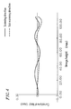
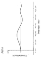
- Figures 4 and 5 show the remaining curvature of field and the f ⁇ characteristics, respectively, obtained in the scanning optics according to the present invention.
Landscapes
- Physics & Mathematics (AREA)
- General Physics & Mathematics (AREA)
- Optics & Photonics (AREA)
- Lenses (AREA)
- Mechanical Optical Scanning Systems (AREA)
Claims (19)
- Optischer Scanner bzw. Abtaster mit einer Lichtquelle (1) einem optischen Deflektor bzw. Ablenkungsvorrichtung (5) zum Scannen bzw. Abtasten eines Lichtstromes (light flux) von der Lichtquelle, einem ersten optischen Bildformungssystem (2, 3, 4), welches zwischen der Lichtquelle und dem optischen Deflektor angeordnet ist, und einem zweiten optischen Bildformungssystem (7, 8), welches zwischen dem optischen Deflektor und einer abzutastenden bzw. scannenden Oberfläche (9) angeordnet ist, wobei das zweite optische Bildformungssystem einen gekrümmten Spiegel (7) umfasst zum Reflektieren eines Lichtstromes von dem optischen Deflektor (5) und eine Korrekturlinse (8) zum Konvergieren bzw. Bündeln des Lichtstromes von dem gekrümmten Spiegel auf die abzutastende bzw. zu scannende Oberfläche, das Brechungsvermögen in der Neben-Scan (sub-scanning) Richtung (x) bei einer Mitte der Korrekturlinse (8) in einer Abtast- bzw. Scan-Richtung (y) ist verschieden von dem Brechungsvermögen in der Neben-Scan-Richtung bei einem Umfang der Korrekturlinse,
wobei wenn ein Abstand zwischen einem Reflexionspunkt des optischen Deflektors bzw. Ablenkungsvorrichtung und einem Reflexionspunkt des gekrümmten Spiegels L(mm) ist, ein Abstand zwischen dem Reflexionspunkt des gekrümmten Spiegels und einer Einfallsoberfläche der Korrekturlinse M(mm) ist, und die Brennweite des zweiten optischen Bildformungssystem in der Scan-Richtung fm(mm) ist, ist die nachfolgende Ungleichung bzw. konditionale Formel (3) erfüllt - Optischer Scanner nach Anspruch 1, wobei eine auftauchende bzw. vorstehende Oberfläche der Korrekturlinse (8) eine zylinderförmige Oberfläche ist, welche ein Brechungsvermögen nur in der Scan-Richtung aufweist.
- Optischer Scanner nach Anspruch 1, wobei eine auftauchende bzw. vorstehende Oberfläche der Korrekturlinse (8) eine asphärische zylinderförmige Oberfläche, welche ein Brechungsvermögen nur in der Scan-Richtung hat und der Abschnitt der Oberfläche in der Scan-Richtung hat Entwicklungs-Terme vierter oder höherer Ordnung.
- Optischer Scanner nach Anspruch 1, wobei wenn eine Brennweite des zweiten optischen Bildformungssystems (7, 8) in der Scan-Richtung fm(mm) ist, eine effektive Scan- bzw. Abtast-Breite der abzutastenden Oberfläche W(mm) ist, ein Abstand zwischen einem Ablenkungs- bzw. Deflektions-Punkt des optischen Deflektors bzw. Ablenkungsvorrichtung (5) und ein Reflexionspunkt des gekrümmten Spiegels (7) L(mm) ist, und ein Abstand zwischen einer effektiven äußersten Position des gekrümmten Spiegels (7) in der Scan- bzw. Abtastrichtung und einer Tangentialebene eines Scheitel- bzw. Eckpunktes der Spiegeloberfläche zm(mm) ist, ist folgende Ungleichung bzw. Konditionalformel (1) erfüllt:
- Optischer Scanner nach Anspruch 1, wobei der gekrümmte Spiegel (7) eine axialsymmetrische asphärische Oberfläche hat.
- Optischer Scanner nach Anspruch 1, wobei wenn ein Abstand bzw. eine Verschiebung eines Scheitel- bzw. Eckpunktes des gekrümmten Spiegels (7) von einer optischen Achse xm(mm) ist, ist nachfolgende Konditionalformel (2) erfüllt:
- Optischer Scanner nach Anspruch 1, wobei ein Winkel βP (Grad) ist, welcher gebildet wird durch eine Ebene senkrecht zu einer Reflexionsoberfläche des optischen Deflektors bzw. Ablenkungsvorrichtung und parallel zu der Scan- bzw. Abtast-Richtung und einer optischen Achse des ersten optischen Bildformungssystems, ein Abstand zwischen einem Reflexionspunkt des optischen Deflektors bzw. Ablenkungsvorrichtung und einem Reflexionspunkt des gekrümmten Spiegel ist L(mm), ein Abstand zwischen dem Reflexionspunkt des gekrümmten Spiegel und der Einfallsoberfläche der Korrekturlinse ist M(mm), eine Brennweite des zweiten optischen Bildformungssystems in der Scan- bzw. Abtast-Richtung ist fm(mm), und ein Abstand bzw. eine Verschiebung eines Mittelpunkts der Einfallsoberfläche der Korrekturlinse von der optischen Achse in der Neben-Scan-Richtung ist xL(mm), und die folgende Konditionalformel (4) ist erfüllt
- Optischer Scanner nach Anspruch 1, wobei ein Winkel, welcher gebildet wird durch eine Ebene senkrecht zu einer Reflexionsoberfläche des optischen Deflektors bzw. Ablenkungsvorrichtung und parallel zu der Scan-Richtung und einer optischen Achse des ersten optischen Bildformungssystems ist βP (Grad), ein Abstand zwischen einem Reflexionspunkt des optischen Deflektors und einem Reflexionspunkt des gekrümmten Spiegels ist L(mm), ein Abstand zwischen dem Reflexionspunkt des gekrümmte Spiegels und einer Einfallsoberfläche der Korrekturlinse ist M(mm), eine Brennweite des zweiten optischen Bildformungssystems in der Scan-Richtung ist fm(mm), und ein Winkel, welcher ausgebildet wird durch eine Senkrechte zu einem Scheitelpunkt bzw. Eckpunkt des gekrümmten Spiegels und der optischen Achse ist βm (Grad), wobei die nachfolgende Konditionalformel (5) erfüllt ist:
- Optischer Scanner nach Anspruch 1, wobei eine Brennweite des zweiten optischen Bildformungssystems in der Scan-Richtung fm(mm) ist, und eine effektive Scan- bzw. Abtast-Breite der abzutastenden Oberfläche ist W(mm), wobei die nachfolgende Konditionalformel (6) erfüllt ist
- Optischer Scanner bzw. Abtaster mit einer Lichtquelle (1), einem optischen Deflektor bzw. Ablenkungsvorrichtung (5) zum Scannen bzw. Abtasten eines Lichtstromes (light flux) von der Lichtquelle, einem ersten optischen Bildformungssystem (2, 3, 4), welches zwischen der Lichtquelle (1) und dem optischen Deflektor angeordnet ist, und, einem zweiten optischen Bildformungssystem (7, 8), welches zwischen dem optischen Deflektor und einer abzutastenden bzw. scannenden Oberfläche (9) angeordnet ist, wobei das zweite optische Bildformungssystem einen gekrümmten Spiegel (7) umfasst zum Reflektieren eines Lichtstromes von dem optischen Deflektor (5) und eine Korrekturlinse (8) zum Korrigieren bzw. Konvergieren bzw. Bündeln des Lichtstromes von dem gekrümmten Spiegel auf die abzutastende bzw. zu scannende Oberfläche, das Brechungsvermögen in der Neben-Scan (sub-scanning) Richtung (x) bei der Mitte der Korrekturlinse in der Abtast- bzw. Scan-Richtung (y) ist verschieden von dem Brechungsvermögen in der Neben-Scan-Richtung bei dem Umfang der Korrekturlinse,
dadurch gekennzeichnet, dass
die Einfallsoberfläche der Korrekturlinse (8) eine torusförmige bzw. Ring-Sattel-Oberfläche ist, mit einem Profil, welches definiert ist durch eine Kurve mit Entwicklungs-Thermen vierter oder höherer Ordnung, welche in der Ebene vorliegt, welche die Scan- bzw. Abtast-Richtung und die optische Achse des optischen Systems enthält, und gedreht ist um eine drehsymmetrische Achse, welche parallel ist zu der Scan- bzw. Abtast-Richtung und in der Ebene liegt, welche die optische Achse umfasst. - Optischer Scanner, nach Anspruch 10, wobei eine auftauchende bzw. vorstehende Oberfläche der Korrekturlinse (8) eine zylinderförmige Oberfläche ist, welche ein Brechungsvermögen nur in der Scan-Richtung aufweist
- Optischer Scanner nach Anspruch 11, wobei eine auftauchende bzw. vorstehende Oberfläche der Korrekturlinse eine asphärische zylinderförmige Oberfläche ist, welche ein Brechungsvermögen nur in der Scan-Richtung hat und der Abschnitt der Oberfläche in der Scan-Richtung hat Entwicklungs-Terme vierter oder höherer Ordnung.
- Optischer Scanner nach Anspruch 12, wobei wobei wenn eine Brennweite des zweiten optischen Bildformungssystems in der Scan-Richtung fm(mm) ist, eine effektive Scan- bzw. Abtast-Breite der abzutastenden Oberfläche W(mm) ist, ein Abstand zwischen einem Ablenkungs- bzw. Deflektions-Punkt des optischen Deflektors bzw. Ablenkungsvorrichtung und einem Reflexionspunkt des gekrümmten Spiegels ist L(mm) ist, und ein Abstand zwischen einer effektiven äußersten Position des gekrümmten Spiegels in der Scan- bzw. Abtastrichtung und einer Tangentialebene eines Scheitel- bzw. Eckpunktes der Spiegeloberfläche zm(mm) ist, ist folgende Ungleichung bzw. Konditionalformel (1) erfüllt:
- Optischer Scanner nach Anspruch 13, wobei wenn ein Abstand bzw. eine Verschiebung eines Scheitel- bzw. Eckpunktes des gekrümmten Spiegels von einer optischen Achse xm(mm) ist, ist nachfolgende Konditionalformel (2) erfüllt:
- Optischer Scanner nach Anspruch 14, wobei wenn ein Abstand zwischen einem Reflexionspunkt des optischen Deflektors bzw. Ablenkungsvorrichtung und einem Reflexionspunkt des gekrümmten Spiegels L(mm) ist, ein Abstand zwischen dem Reflexionspunkt des gekrümmten Spiegels und einer Einfallsoberfläche der Korrekturlinse M(mm) ist, und die Brennweite des zweiten optischen Bildformungssystems in der Scan-Richtung fm(mm) ist, ist die nachfolgende Ungleichung bzw. Konditionalformel (3) erfüllt:
- Optischer Scanner nach Anspruch 15, wobei ein Winkel βP (Grad) ist, welcher gebildet wird durch eine Ebene senkrecht zu einer Reflexionsoberfläche des optischen Deflektors bzw. Ablenkungsvorrichtung und parallel zu der Scan- bzw. Abtast-Richtung und einer optischen Achse des ersten optischen Bildformungssystems, ein Abstand zwischen einem Reflexionspunkt des optischen Deflektors bzw. Ablenkungsvorrichtung und einem Reflexionspunkt des gekrümmten Spiegel ist L(mm), ein Abstand zwischen dem Reflexionspunkt des gekrümmten Spiegel und der Einfallsoberfläche der Korrekturlinse ist M(mm), eine Brennweite des zweiten optischen Bildformungssystems in der Scan- bzw. Abtast-Richtung ist fm(mm), und ein Abstand bzw. eine Verschiebung eines Mittelpunkts der Einfallsoberfläche der Korrekturlinse von der optischen Achse in der Neben-Scan-Richtung ist xL(mm), und die folgende Konditionalformel (4) ist erfüllt::
- Optischer Scanner nach Anspruch 16, wobei ein Winkel, welcher gebildet wird durch eine Ebene senkrecht zu einer Reflexionsoberfläche des optischen Deflektors bzw. Ablenkungsvorrichtung und parallel zu der Scan-Richtung und einer optischen Achse des ersten optischen Bildformungssystems ist βP (Grad), ein Abstand zwischen einem Reflexionspunkt des optischen Deflektors und einem Reflexionspunkt des gekrümmten Spiegels ist L(mm), ein Abstand zwischen dem Reflexionspunkt des gekrümmte Spiegels und einer Einfallsoberfläche der Korrekturlinse ist M(mm), eine Brennweite des zweiten optischen Bildformungssystems in der Scan-Richtung ist fm(mm), und ein Winkel, welcher ausgebildet wird durch eine Senkrechte zu einem Scheitelpunkt bzw. Eckpunkt des gekrümmten Spiegels und der optischen Achse ist βm (Grad), wobei die nachfolgende Konditionalformel (5) erfüllt ist:
- Optischer Scanner nach Anspruch 17, wobei eine Brennweite des zweiten optischen Bildformungssystems in der Scan-Richtung fm(mm) ist, und eine effektive Scan- bzw. Abtast-Breite der abzutastenden Oberfläche ist W(mm), wobei die nachfolgende Konditionalformel (6) erfüllt ist
- Bildformungsvorrichtung, welche den optischen Scanner nach Anspruch 1 verwendet
Applications Claiming Priority (3)
| Application Number | Priority Date | Filing Date | Title |
|---|---|---|---|
| JP17684794A JP3275548B2 (ja) | 1994-07-28 | 1994-07-28 | 光走査装置 |
| JP17684794 | 1994-07-28 | ||
| JP176847/94 | 1994-07-28 |
Publications (3)
| Publication Number | Publication Date |
|---|---|
| EP0694802A2 EP0694802A2 (de) | 1996-01-31 |
| EP0694802A3 EP0694802A3 (de) | 1998-01-14 |
| EP0694802B1 true EP0694802B1 (de) | 2001-12-12 |
Family
ID=16020876
Family Applications (1)
| Application Number | Title | Priority Date | Filing Date |
|---|---|---|---|
| EP95111758A Expired - Lifetime EP0694802B1 (de) | 1994-07-28 | 1995-07-26 | Optischer Abtaster |
Country Status (4)
| Country | Link |
|---|---|
| US (1) | US5657147A (de) |
| EP (1) | EP0694802B1 (de) |
| JP (1) | JP3275548B2 (de) |
| DE (1) | DE69524492T2 (de) |
Families Citing this family (6)
| Publication number | Priority date | Publication date | Assignee | Title |
|---|---|---|---|---|
| US6400442B1 (en) * | 1996-08-28 | 2002-06-04 | Polaroid Corporation | Optical system for use in a photographic printer |
| KR20010014242A (ko) * | 1997-07-08 | 2001-02-26 | 게스레이 마크 | 레이저 스캐너용 왜상 스캔 렌즈 |
| IL133243A0 (en) | 1999-03-30 | 2001-03-19 | Univ Ramot | A method and system for super resolution |
| JP2001318331A (ja) * | 2000-05-09 | 2001-11-16 | Asahi Optical Co Ltd | 反射型走査光学系 |
| US6344893B1 (en) | 2000-06-19 | 2002-02-05 | Ramot University Authority For Applied Research And Industrial Development Ltd. | Super-resolving imaging system |
| CN112114425B (zh) * | 2020-09-14 | 2022-06-07 | 福建福光股份有限公司 | 一种扫描型中波红外光学系统 |
Citations (1)
| Publication number | Priority date | Publication date | Assignee | Title |
|---|---|---|---|---|
| US5408095A (en) * | 1992-07-22 | 1995-04-18 | Ricoh Company, Ltd. | Optical scanner having an image forming mirror and means for reducing scanning line pitch irregularities |
Family Cites Families (11)
| Publication number | Priority date | Publication date | Assignee | Title |
|---|---|---|---|---|
| EP0078269A4 (de) * | 1981-02-23 | 1983-06-15 | Gen Optronics Corp | Beugungsgitterscanner mit anamorphotischer korrektion der abtastkurven. |
| JPS62127819A (ja) * | 1985-11-29 | 1987-06-10 | Konishiroku Photo Ind Co Ltd | 走査光学系 |
| JP2615850B2 (ja) * | 1988-05-27 | 1997-06-04 | ミノルタ株式会社 | 光ビーム走査光学系 |
| JPH01300218A (ja) * | 1988-05-27 | 1989-12-04 | Minolta Camera Co Ltd | 光ビーム走査光学系 |
| JPH0215231A (ja) * | 1988-07-04 | 1990-01-18 | Sankyo Seiki Mfg Co Ltd | 走査光学系 |
| JPH0769521B2 (ja) * | 1988-07-13 | 1995-07-31 | 株式会社日立製作所 | 光走査装置及び走査レンズ |
| JP2598473B2 (ja) * | 1988-08-01 | 1997-04-09 | 株式会社リコー | 走査光学系 |
| JP2682675B2 (ja) * | 1988-11-07 | 1997-11-26 | 株式会社リコー | 走査光学系 |
| JP2964629B2 (ja) * | 1990-11-22 | 1999-10-18 | ミノルタ株式会社 | レーザビーム走査光学装置 |
| US5426298A (en) * | 1992-03-17 | 1995-06-20 | Ricoh Company, Ltd. | Optical scanner |
| JP3266725B2 (ja) * | 1993-12-29 | 2002-03-18 | 旭光学工業株式会社 | 走査光学系 |
-
1994
- 1994-07-28 JP JP17684794A patent/JP3275548B2/ja not_active Expired - Fee Related
-
1995
- 1995-07-24 US US08/505,974 patent/US5657147A/en not_active Expired - Lifetime
- 1995-07-26 DE DE69524492T patent/DE69524492T2/de not_active Expired - Fee Related
- 1995-07-26 EP EP95111758A patent/EP0694802B1/de not_active Expired - Lifetime
Patent Citations (1)
| Publication number | Priority date | Publication date | Assignee | Title |
|---|---|---|---|---|
| US5408095A (en) * | 1992-07-22 | 1995-04-18 | Ricoh Company, Ltd. | Optical scanner having an image forming mirror and means for reducing scanning line pitch irregularities |
Also Published As
| Publication number | Publication date |
|---|---|
| EP0694802A3 (de) | 1998-01-14 |
| DE69524492T2 (de) | 2002-07-18 |
| DE69524492D1 (de) | 2002-01-24 |
| JP3275548B2 (ja) | 2002-04-15 |
| EP0694802A2 (de) | 1996-01-31 |
| US5657147A (en) | 1997-08-12 |
| JPH0843753A (ja) | 1996-02-16 |
Similar Documents
| Publication | Publication Date | Title |
|---|---|---|
| US6388792B1 (en) | Optical scanning device and image forming apparatus | |
| JP4717285B2 (ja) | 走査光学装置及びそれを用いた画像形成装置 | |
| JP3330248B2 (ja) | 光走査装置、画像形成装置及び画像読み取り装置 | |
| EP0853253B1 (de) | Optisches Abtastgerät | |
| JP5116559B2 (ja) | 光走査装置及びそれを用いた画像形成装置 | |
| KR20010107742A (ko) | 광학 주사 장치와 이를 사용하는 화상 형성 장치 | |
| JPH05241094A (ja) | ポストオブジェクティブ型走査光学系と画像形成装置 | |
| US8400699B2 (en) | Optical scanning device and image forming apparatus using the same | |
| JP4684470B2 (ja) | 光走査装置及びそれを用いた画像形成装置 | |
| US20030043442A1 (en) | Scanning optical apparatus and image forming apparatus using the same | |
| JP4659277B2 (ja) | 光走査装置及びそれを用いた画像形成装置 | |
| JP3420956B2 (ja) | 光走査装置及びこれを用いた画像読取装置と画像形成装置 | |
| JPH07113950A (ja) | 光ビーム走査装置及び結像レンズ | |
| JP3943820B2 (ja) | 光走査装置及びマルチビーム光走査装置及び画像形成装置 | |
| EP0694802B1 (de) | Optischer Abtaster | |
| US20040109212A1 (en) | Optical scanning apparatus and image forming apparatus using the same | |
| JP2008170487A (ja) | 光走査装置及びそれを用いた画像形成装置 | |
| JPH07318832A (ja) | 走査光学系およびそれを用いた画像形成装置 | |
| JPH07174998A (ja) | 走査レンズ及び光走査装置 | |
| JP2956169B2 (ja) | 走査光学装置 | |
| JP2003156704A (ja) | 光走査装置及びそれを用いた画像形成装置 | |
| JP4817526B2 (ja) | 光走査装置及びそれを用いた画像形成装置 | |
| JP2773593B2 (ja) | 光ビーム走査光学系 | |
| JP3390118B2 (ja) | 光走査装置、それを用いた画像読取り装置及び画像形成装置 | |
| JP4551569B2 (ja) | 光走査装置及びそれを用いた画像形成装置 |
Legal Events
| Date | Code | Title | Description |
|---|---|---|---|
| PUAI | Public reference made under article 153(3) epc to a published international application that has entered the european phase |
Free format text: ORIGINAL CODE: 0009012 |
|
| 17P | Request for examination filed |
Effective date: 19950726 |
|
| AK | Designated contracting states |
Kind code of ref document: A2 Designated state(s): DE FR GB IT NL |
|
| PUAL | Search report despatched |
Free format text: ORIGINAL CODE: 0009013 |
|
| AK | Designated contracting states |
Kind code of ref document: A3 Designated state(s): DE FR GB IT NL |
|
| 17Q | First examination report despatched |
Effective date: 19980828 |
|
| GRAG | Despatch of communication of intention to grant |
Free format text: ORIGINAL CODE: EPIDOS AGRA |
|
| GRAG | Despatch of communication of intention to grant |
Free format text: ORIGINAL CODE: EPIDOS AGRA |
|
| GRAH | Despatch of communication of intention to grant a patent |
Free format text: ORIGINAL CODE: EPIDOS IGRA |
|
| GRAH | Despatch of communication of intention to grant a patent |
Free format text: ORIGINAL CODE: EPIDOS IGRA |
|
| GRAA | (expected) grant |
Free format text: ORIGINAL CODE: 0009210 |
|
| AK | Designated contracting states |
Kind code of ref document: B1 Designated state(s): DE FR GB IT NL |
|
| REG | Reference to a national code |
Ref country code: GB Ref legal event code: IF02 |
|
| REF | Corresponds to: |
Ref document number: 69524492 Country of ref document: DE Date of ref document: 20020124 |
|
| ET | Fr: translation filed | ||
| PLBE | No opposition filed within time limit |
Free format text: ORIGINAL CODE: 0009261 |
|
| STAA | Information on the status of an ep patent application or granted ep patent |
Free format text: STATUS: NO OPPOSITION FILED WITHIN TIME LIMIT |
|
| 26N | No opposition filed | ||
| PGFP | Annual fee paid to national office [announced via postgrant information from national office to epo] |
Ref country code: NL Payment date: 20060716 Year of fee payment: 12 |
|
| PGFP | Annual fee paid to national office [announced via postgrant information from national office to epo] |
Ref country code: FR Payment date: 20060719 Year of fee payment: 12 |
|
| PGFP | Annual fee paid to national office [announced via postgrant information from national office to epo] |
Ref country code: DE Payment date: 20060720 Year of fee payment: 12 |
|
| PGFP | Annual fee paid to national office [announced via postgrant information from national office to epo] |
Ref country code: GB Payment date: 20060726 Year of fee payment: 12 |
|
| PGFP | Annual fee paid to national office [announced via postgrant information from national office to epo] |
Ref country code: IT Payment date: 20060731 Year of fee payment: 12 |
|
| GBPC | Gb: european patent ceased through non-payment of renewal fee |
Effective date: 20070726 |
|
| NLV4 | Nl: lapsed or anulled due to non-payment of the annual fee |
Effective date: 20080201 |
|
| PG25 | Lapsed in a contracting state [announced via postgrant information from national office to epo] |
Ref country code: NL Free format text: LAPSE BECAUSE OF NON-PAYMENT OF DUE FEES Effective date: 20080201 Ref country code: DE Free format text: LAPSE BECAUSE OF NON-PAYMENT OF DUE FEES Effective date: 20080201 |
|
| PG25 | Lapsed in a contracting state [announced via postgrant information from national office to epo] |
Ref country code: GB Free format text: LAPSE BECAUSE OF NON-PAYMENT OF DUE FEES Effective date: 20070726 |
|
| REG | Reference to a national code |
Ref country code: FR Ref legal event code: ST Effective date: 20080331 |
|
| PG25 | Lapsed in a contracting state [announced via postgrant information from national office to epo] |
Ref country code: FR Free format text: LAPSE BECAUSE OF NON-PAYMENT OF DUE FEES Effective date: 20070731 |
|
| PG25 | Lapsed in a contracting state [announced via postgrant information from national office to epo] |
Ref country code: IT Free format text: LAPSE BECAUSE OF NON-PAYMENT OF DUE FEES Effective date: 20070726 |