EP0695028A2 - Signalsummiereinrichtung in kleinem Massstab und differentielle Detektionseinrichtung - Google Patents
Signalsummiereinrichtung in kleinem Massstab und differentielle Detektionseinrichtung Download PDFInfo
- Publication number
- EP0695028A2 EP0695028A2 EP95305195A EP95305195A EP0695028A2 EP 0695028 A2 EP0695028 A2 EP 0695028A2 EP 95305195 A EP95305195 A EP 95305195A EP 95305195 A EP95305195 A EP 95305195A EP 0695028 A2 EP0695028 A2 EP 0695028A2
- Authority
- EP
- European Patent Office
- Prior art keywords
- data
- selector
- signal
- quadrature
- inphase
- Prior art date
- Legal status (The legal status is an assumption and is not a legal conclusion. Google has not performed a legal analysis and makes no representation as to the accuracy of the status listed.)
- Granted
Links
Images





Classifications
-
- H—ELECTRICITY
- H03—ELECTRONIC CIRCUITRY
- H03D—DEMODULATION OR TRANSFERENCE OF MODULATION FROM ONE CARRIER TO ANOTHER
- H03D3/00—Demodulation of angle-, frequency- or phase- modulated oscillations
- H03D3/007—Demodulation of angle-, frequency- or phase- modulated oscillations by converting the oscillations into two quadrature related signals
-
- H—ELECTRICITY
- H03—ELECTRONIC CIRCUITRY
- H03D—DEMODULATION OR TRANSFERENCE OF MODULATION FROM ONE CARRIER TO ANOTHER
- H03D2200/00—Indexing scheme relating to details of demodulation or transference of modulation from one carrier to another covered by H03D
- H03D2200/0041—Functional aspects of demodulators
- H03D2200/005—Analog to digital conversion
-
- H—ELECTRICITY
- H03—ELECTRONIC CIRCUITRY
- H03D—DEMODULATION OR TRANSFERENCE OF MODULATION FROM ONE CARRIER TO ANOTHER
- H03D2200/00—Indexing scheme relating to details of demodulation or transference of modulation from one carrier to another covered by H03D
- H03D2200/0041—Functional aspects of demodulators
- H03D2200/006—Signal sampling
- H03D2200/0062—Computation of input samples, e.g. successive samples
-
- H—ELECTRICITY
- H03—ELECTRONIC CIRCUITRY
- H03D—DEMODULATION OR TRANSFERENCE OF MODULATION FROM ONE CARRIER TO ANOTHER
- H03D3/00—Demodulation of angle-, frequency- or phase- modulated oscillations
- H03D3/006—Demodulation of angle-, frequency- or phase- modulated oscillations by sampling the oscillations and further processing the samples, e.g. by computing techniques
Definitions
- This invention relates to a signal adding device for adding received multiple signals in digital signal processing and also relates to a differential detecting device that handles phase-modulated signals with the above signal adding device, and specifically relates to a signal adding device and differential detecting device realized in small-scale logical circuits.
- differential detecting devices handling phase-modulated signals have often been used. This is because the differential detecting method is less affected by a phenomenon called fading, a disturbance unique to mobile communications.
- Japanese Laid-Open Patent Application No.63-153942 and Japanese Laid-Open Utility Model No.2-70542 disclose techniques concerning differential detecting devices in digital signal processing. These prior-art differential detecting devices are explained below with reference to the drawings.
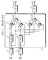
- Fig.1 shows a structure of a prior-art differential detecting device.
- 21 and 22 represent A/D converters that sample inphase and quadrature-phase baseband signals i(t) and q(t).
- Inphase and quadrature-phase baseband signals i(t) and q(t) are obtained by performing the quasi-synchronous quadrature-phase detection on the modulated signal; that means, by multiplying the input signal with two respective local signals having the same frequency as the input carrier wave and differing each other by angle of 90 degrees.
- Differential detection calculating unit 33 comprises delays 23 and 24, multipliers 25, 26, 27, and 28, and adders 29 and 30.
- 31 and 32 represent lowpass filters. The differential detecting device with the above composition is explained below on its operation.
- sampled quadrature-phase baseband signal Q(nT) sampled by A/D converter 22 goes two ways, one of which directly enters multiplier 26, and the other is delayed by delay 24 one symbol time mt to change to Q ⁇ (n-m)T ⁇ then enters multiplier 26.
- Adder 29 adds the outputs from multiplier 25 and 26 and outputs detection output E1(nT).
- Adder 30 outputs another detection output E2(nT) with the following procedure: first, outputs from delay 23 and A/D converter 22 are input to multiplier 27, then outputs from delay 24 and A/D converter 21 are input to multiplier 28, and outputs from the multiplier 27 and 28 are input to adder 30 which outputs E2(nT). In this way, vector calculations on sampling baseband signals I(nT)+jQ(nT) and I ⁇ (n-m)T ⁇ +jQ ⁇ (n-m)T ⁇ , where j is an imaginary number, are performed to detect the phase difference.
- detection outputs E1(nT) and E2(nT) from respective adders 29 and 30 are input to lowpass filters 31 and 32 respectively, by which unnecessary high-frequency elements generated by A/D converters 21 and 22 in digitization are filtered to gain demodulated baseband signals C1(nT) C2(nT).
- the prior-art differential detecting device performs the differential detection by digitizing the phase-modulated signal and then by performing the vector calculations shown in Formula 2.
- the first object of the present invention in consideration of the above mentioned problems, is to provide a signal adding device with small-scale logical circuit.
- the second object of the present invention is to provide a differential detecting device easily put into IC, which is enabled by reducing the hardware components required for vector calculations.
- the first object is achieved by a signal adding device for adding n input signals with frequency fb or lower and outputting an added signal, fb being a real number, and n being an integer greater than 0, comprising: a multiplexing unit for multiplexing the n input signals in time-division at time ⁇ t intervals, multiplexing all the n input signals at least once, ⁇ t being 1/2nfb or shorter; and a lowpass filter for cutting frequency components with frequency (1/n ⁇ t)-fb or higher from signals output from the multiplexing unit and passing frequency components with frequency fb or lower; and an outputting unit for outputting signals which have passed the lowpass filter as the added signal.
- the multiplexing unit of the device may comprise: an analog signal selector for selecting each of the n input signals in sequence and selecting all the n input signals in time period 1/2fb or shorter; and an A/D converter for sampling and digitizing each of the input signals output from the analog signal selector, and outputting sampled digital signals to the lowpass filter.
- the multiplexing unit of the device may also comprise: n A/D converters each of which samples and digitizes a corresponding one of the n input signals at every time period n ⁇ t and outputs m-bit data, n ⁇ t being 1/2nfb or shorter, the n A/D converters performing sampling with time difference ⁇ t between each other, m being an integer greater than 0; and a selector which, synchronized with digitizations by the n A/D converters, sequentially selects one from n pieces of the m-bit data output from the n A/D converters and outputting selected m-bit data to the lowpass filter.
- a differential detecting device for detecting, from inphase and quadrature-phase baseband signals which are obtained by a quadrature detection on a phase-modulated signal, cosine and sine components of a phase difference at two instants of the phase-modulated signal, comprising: two A/D converters for digitizing and converting the inphase and quadrature-phase baseband signals to respective inphase data and quadrature-phase data at every predetermined time period (symbol); a cosine component calculating unit for multiplying the inphase data by previous inphase data predetermined symbols earlier, multiplying the quadrature-phase data by previous quadrature-phase data the predetermined symbols earlier, and alternately outputting their multiplication results at every symbol in time-division multiplexing; a sine component calculating unit for multiplying the quadrature-phase data by inphase data the predetermined symbols earlier, multiplying the inphase data by quadrature-phase data the predetermined symbols earlier, and alternately outputting their multiplication results at every symbol in time-division multiplexing;
- the cosine component calculating unit of the device may also comprise: a first selector for selecting the inphase data and the quadrature-phase data alternately at every symbol; a delay for delaying data selected by the first selector for the predetermined number of symbols; and a first multiplier for multiplying data selected by the first selector by data delayed by the delay
- the sine component calculating unit comprises: a second selector, operating synchronously with the first selector, for selecting the quadrature-phase data when the first selector selects the inphase data, and selecting the inphase data when the first selector selects the quadrature-phase data; an inverter for inverting and outputting the inphase data selected by the second selector and outputting the quadrature-phase data selected by the second selector as it is; and a second multiplier for multiplying data output from the inverter by data delayed by the delay.
- Fig.2 is a block diagram illustrating the structure of the differential detecting device in First Embodiment of the present invention.
- Fig.3 is a block diagram illustrating the structure of the differential detection calculating unit in First Embodiment of the present invention.
- Fig.5 shows the wave forms of the detection signals and demodulated baseband signals in First Embodiment of the present invention.
- Fig.6 is a block diagram illustrating the structure of the differential detecting device in Second Embodiment of the present invention.
- Fig.8 is a block diagram illustrating the structure of a prior-art signal adding device.
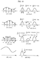
- Fig.10 shows the wave forms and frequency spectra for explaining the addition principles of the signal adding device in Third Embodiment of the present invention.
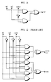
- Fig.11 shows selector 11 in Fig.7 realized in a circuit with gates.
- Fig.12 shows adder 29 in Fig.8 realized in a circuit with gates.
- Fig.13 is a block diagram illustrating the structure of a variation of the signal adding device in Third Embodiment of the present invention.
- Fig.14 shows the circuit of selector 33 for analog signals used in the variation of the signal adding device shown in Fig.13.
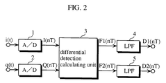
- Fig.2 is a block diagram illustrating the structure of the differential detecting device in the first embodiment of the present invention.
- 1 represents first A/D converter, 2 second A/D converter, 3 differential detection calculating unit, 4 first lowpass filter, and 5 second lowpass filter.
- First A/D converter 1 samples inphase baseband signal i(t), and inputs sampled baseband signal I(nT) to differential detection calculating unit 3.
- Second A/D converter 2 samples quadrature-phase baseband signal q(t), and inputs sampled baseband signal Q(nT) to differential detection calculating unit 3.
- Differential detection calculating unit 3 performs the calculations shown in Formula 3 below on the sampled baseband signals I(nT) and Q(nT), inputs detection signal F1(nT) to first lowpass filter 4, and F2(nT) to second lowpass filter 5.
- First lowpass filter 4 and second lowpass filter 5 lowpass-filter detection signals F1(nT) and F2(nT) and obtain demodulated baseband signals D1(nT) and D2(nT) respectively.
- first A/D converter 1 and second A/D converter 2 output eight-bit data respectively, and as for input/output of differential detection calculating unit 3, and inputs of first lowpass filter 4 and second lowpass filter 5, data is passed over the eight-bit buses.
- the components 3, 4, and 5 are realized in logical circuits that handle eight-bit data. Though it is not described in the figure, a clock oscillator sends a clock signal to each component so that it can operate synchronously with the signal.
- Fig.3 illustrates the structure of the differential detection calculating unit 3.
- the differential detection calculating unit 3 comprises first selector 11, second selector 12, delay 13, inverter 14, first multiplier 15, second multiplier 16, and select signal generator 18, and performs the calculations shown in Formula 3.
- Both sampled baseband signals I(nT) and Q(nT) are input to first selector 11 and second selector 12 respectively.
- Sampled baseband signal I(nT) is inverted by inverter 14 to - I(nT) before it is input to second selector 12.
- First selector 11 operates synchronously with the clock signal from select signal generator 18, and outputs data S1(nT) by selecting alternately I(nT) and Q(nT) which are input simultaneously at every sampling period T.
- second selector 12 operates synchronously with the clock signal from select signal generator 18, but selects alternately -I(nT) and Q(nT) to output data S2(nT).
- Output data S1(nT) of first selector 11 goes two ways, one of which directly enters first multiplier 15, the other is delayed one symbol time mT by delay 13 to change to S1 ⁇ (n-m)T ⁇ and goes two ways to enter first multiplier 15 and second multiplier 16.
- output S2(nT) of second selector 12 directly enters second multiplier 16.
- the outputs of the selectors are shown in Formula 4.
- output F1(nT) of first multiplier 15 can be expressed as Formula 5.
- Detection signals F1(nT) and F2(nT) are generated as above. Now, it is assumed that the sampling speed in the present embodiment is twice that of the prior art.
- Fig.4 is a table showing the time-series change of detection signals F1(nT) and F2(nT). Detection signals E1(nT) and E2(nT) of the prior art are shown for comparison. It is assumed that integer n takes the values from 1 to 8 and m, number of samples per one symbol, is 4.
- detection signal F2(nT) alternately takes multiplication results of sampled inphase and quadrature-phase baseband signals, namely I ⁇ (n-m)T ⁇ •Q(nT) and -I(nT)•Q ⁇ (n-m)T ⁇ .
- prior-art detection signal E2(nT) takes the addition result of I ⁇ (n-m)T ⁇ •Q(nT) and -I(nT)•Q ⁇ (n-m)T ⁇ .
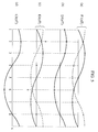
- Fig.5 shows waveforms of detection signal F1(nT), prior-art detection signal E1(nT), demodulated baseband signal D1(nT), and prior art demodulated baseband signal C1(nT). It is assumed as in Fig.4 that integer n takes the values from 1 to 8 and m is 4.
- signs ⁇ in (c) represent the values of prior-art detection signal E1(nT), each of which is the addition result of the multiplication result of sampled inphase baseband signals, I(nT)•I ⁇ (n-m)T ⁇ , and the multiplication result of sampled quadrature-phase baseband signals, Q(nT)•Q ⁇ (n-m)T ⁇ .
- Signs ⁇ on smoothed continuous line in (d) represent the values of prior-art demodulated baseband signal C1(nT), which is the lowpass-filtered detection signal E1(nT).
- signs ⁇ on smoothed continuous line in (b) represent the values of demodulated baseband signal D1(nT), which is the lowpass-filtered detection signal F1(nT).
- the continuous line in (b) and (d) are the same, as it is understood by comparing them. Consequently, it can be said that lowpass-filtering detection signal F1(nT) in (a) has generated baseband signal D1(nT), which is equal to prior-art demodulated baseband signal C1(nT).
- the differential detecting device in the second embodiment of the present invention is explained with reference to the figures.
- the structure of the differential detecting device in the second embodiment is the same as the block diagram in Fig.2.
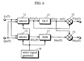
- Fig.6 shows the structure of differential detection calculating unit 3.
- the differential detection calculating unit 3 comprises first selector 11, second selector 12, delay 13, inverter 17, first multiplier 15, second multiplier 16, and select signal generator 18, for performing the calculations in Formula 3.
- the structure of the device in the present embodiment is almost the same as that in the first embodiment except newly added inverter 17. So, the other components have the same numbers as the first embodiment.
- Inverter 17 alternately outputs inverted data and non-inverted data. Practically, such a circuit which deals with one-bit data is the two-input exclusive OR.
- the exclusive OR operates as follows: if one of the inputs is H, the other input is inverted and output; and if L, the other not inverted and output as it is.
- Both sampled baseband signals I(nT) and Q(nT) are input respectively to both first selector 11 and second selector 12.
- First selector 11 operates synchronously with the clock signal from select signal generator 18, and outputs data S1(nT) by selecting alternately I(nT) and Q(nT) which are input simultaneously at every sampling period T.
- second selector 12 also operates synchronously with the clock signal from select signal generator 18, but selects I(nT) and Q(nT) being different from that selected by first selector 11, to output data S3(nT).
- output F4(nT) of second multiplier 16 is equal to F2(nT) shown in Formula 6.
- the demodulated baseband signals are generated from the detection signals the same as First Embodiment.
- the input/output signals to/from first selector 11 and second selector 12 are equal to each other in the present embodiment. This enables reduction in gates when the selectors are realized in IC.
- Fig.7 is a block diagram showing the structure of the present device. The components and their numbers are the same as those in First Embodiment.
- the present device adds signals x1(t) and x2(t) in digital signal processing.
- the two signals x1(t) and x2(t) are sampled alternately at every time period T by first and second A/D converters and output as sampled signals x1s(t) and x2s(t) respectively.
- the sampled signals are added to signal zs(t) by selector 11 then input to lowpass filter 4.
- Lowpass filter 4 outputs signal w(t), which is the desired added signal.
- (a1) and (a2) in Fig.10 represent respectively time-base wave form x1s(t) and its frequency spectrum X1s(f);
- (b1) and (b2) represent time-base wave form x2s(t) and its frequency spectrum X2s(f);
- (c1) and (c2) represent time-base wave form zs(t) and its frequency spectrum Zs(f); and
- (d1) and (d2) represent time-base wave form w(t) and its frequency spectrum W(f).
- sampled signal x1s(t) is equal to sampled signal x'1s(t) of the prior art.
- sampled signal x2s(t) is sampled time T later than sampled signal x'2s(t).
- sampled signal xs(t) sampled ⁇ T period later than time 2nT and its Fourier-transformed Xs(f) are expressed as Formula 10 below. From the above fact it follows that the spectrum of (b2) Fig.10 can be obtained.
- the signal adding device in the present device requires less gates than the prior art, and it eases realizing the device in IC.
Landscapes
- Engineering & Computer Science (AREA)
- Power Engineering (AREA)
- Digital Transmission Methods That Use Modulated Carrier Waves (AREA)
- Analogue/Digital Conversion (AREA)
Applications Claiming Priority (3)
| Application Number | Priority Date | Filing Date | Title |
|---|---|---|---|
| JP17547894A JP3166494B2 (ja) | 1994-07-27 | 1994-07-27 | 遅延検波方法および装置 |
| JP17547894 | 1994-07-27 | ||
| JP175478/94 | 1994-07-27 |
Publications (3)
| Publication Number | Publication Date |
|---|---|
| EP0695028A2 true EP0695028A2 (de) | 1996-01-31 |
| EP0695028A3 EP0695028A3 (de) | 1997-04-02 |
| EP0695028B1 EP0695028B1 (de) | 2004-12-15 |
Family
ID=15996752
Family Applications (1)
| Application Number | Title | Priority Date | Filing Date |
|---|---|---|---|
| EP95305195A Expired - Lifetime EP0695028B1 (de) | 1994-07-27 | 1995-07-25 | Signalsummiereinrichtung in kleinem Massstab und differentielle Detektionseinrichtung |
Country Status (5)
| Country | Link |
|---|---|
| US (1) | US5712879A (de) |
| EP (1) | EP0695028B1 (de) |
| JP (1) | JP3166494B2 (de) |
| CA (1) | CA2154646C (de) |
| DE (1) | DE69533852T2 (de) |
Cited By (3)
| Publication number | Priority date | Publication date | Assignee | Title |
|---|---|---|---|---|
| EP0771097A3 (de) * | 1995-10-24 | 2001-02-28 | Matsushita Electric Industrial Co., Ltd. | Differentialdetektor für PSK-Signale |
| EP1217724A1 (de) * | 2000-12-21 | 2002-06-26 | STMicroelectronics S.r.l. | Quadratur-Demodulator |
| GB2418084A (en) * | 2004-09-13 | 2006-03-15 | Filtronic Plc | Method for measuring frequency using digital components |
Families Citing this family (8)
| Publication number | Priority date | Publication date | Assignee | Title |
|---|---|---|---|---|
| EP0849154B1 (de) | 1996-12-20 | 2003-05-14 | Shimano Inc. | Hohltretlagereinheit |
| JP3007580B2 (ja) * | 1996-12-20 | 2000-02-07 | 株式会社シマノ | 軸受の伸縮リテーナー |
| US6539063B1 (en) * | 1999-02-18 | 2003-03-25 | Ibiquity Digital Corporation | System and method for recovering symbol timing offset and carrier frequency error in an OFDM digital audio broadcast system |
| CN1187905C (zh) * | 1999-05-10 | 2005-02-02 | 因芬尼昂技术股份公司 | 用于通信终端设备的接收机电路和在接收机电路中进行信号处理的方法 |
| US6580729B1 (en) * | 1999-11-29 | 2003-06-17 | General Signal Corporation | Signal multiplexer and method |
| US6804306B2 (en) * | 2000-01-11 | 2004-10-12 | Tektronix, Inc. | Stable in-phase/quadrature (I/Q) generator method and apparatus |
| US7177617B2 (en) * | 2003-12-30 | 2007-02-13 | Silicon Laboratories | Method and apparatus for enhancing signal quality within a wireless receiver |
| US7362694B2 (en) * | 2004-05-14 | 2008-04-22 | Broadcom Corporation | Programmable identity of I and Q channels |
Citations (2)
| Publication number | Priority date | Publication date | Assignee | Title |
|---|---|---|---|---|
| JPS63153942A (ja) | 1986-12-18 | 1988-06-27 | Kokusai Electric Co Ltd | デイジタル遅延検波回路 |
| JPH0270542U (de) | 1988-11-16 | 1990-05-29 |
Family Cites Families (21)
| Publication number | Priority date | Publication date | Assignee | Title |
|---|---|---|---|---|
| US3668291A (en) * | 1971-01-22 | 1972-06-06 | Bell Telephone Labor Inc | Pulse code modulation multiplex system |
| US3967069A (en) * | 1972-12-29 | 1976-06-29 | Matsushita Electric Corporation Of America | Compatible four channel FM system |
| US3818143A (en) * | 1973-01-02 | 1974-06-18 | Gte Automatic Electric Lab Inc | Self-stabilizing multiplexing arrangement |
| US3838296A (en) * | 1973-10-29 | 1974-09-24 | Nat Semiconductor Corp | Emitter coupled logic transistor circuit |
| US4184052A (en) * | 1978-01-16 | 1980-01-15 | Texas Instruments Incorporated | AM/FM time division surface wave device transmitter |
| JPS58184822A (ja) * | 1982-03-31 | 1983-10-28 | Fujitsu Ltd | 入力回路 |
| CA1191905A (en) * | 1982-06-30 | 1985-08-13 | Canadian Patents And Development Limited/Societe Canadienne Des Brevets Et D'exploitation Limitee | Spread spectrum modem |
| US4546389A (en) * | 1984-01-03 | 1985-10-08 | Rca Corporation | Video disc encoding and decoding system providing intra-field track error correction |
| JPS6125392A (ja) * | 1984-07-16 | 1986-02-04 | Canon Inc | カラ−ビデオ信号処理装置 |
| US4893316A (en) * | 1985-04-04 | 1990-01-09 | Motorola, Inc. | Digital radio frequency receiver |
| US4740997A (en) * | 1985-08-05 | 1988-04-26 | Hayes Microcomputer Products, Inc. | Band clock offset phase locked loop |
| US4755761A (en) * | 1986-06-26 | 1988-07-05 | General Electric Company | Zero intermediate-frequency demodulator |
| US4809203A (en) * | 1986-08-25 | 1989-02-28 | Ford Aerospace & Communications Corporation | Hybrid analog-digital filter |
| JPH0619470B2 (ja) * | 1988-07-26 | 1994-03-16 | 大和製衡株式会社 | 金属等の異物混入検出方法および検出器 |
| US5007068A (en) * | 1988-06-07 | 1991-04-09 | The United States Of America As Represented By The Administrator Of The National Aeronautics And Space Administration | Doppler-corrected differential detection system |
| JPH0773219B2 (ja) * | 1988-06-16 | 1995-08-02 | 富士通株式会社 | 並直列変換装置 |
| US4965810A (en) * | 1988-11-17 | 1990-10-23 | Plessey Electronics Systems Corp. | Digital differential phase-shift keyed decoder |
| JP2975041B2 (ja) * | 1990-03-27 | 1999-11-10 | 株式会社日立製作所 | ディジタル信号処理プロセッサ |
| JPH05103027A (ja) * | 1991-10-03 | 1993-04-23 | Toshiba Corp | 遅延検波回路 |
| JP2959286B2 (ja) * | 1992-07-02 | 1999-10-06 | 株式会社村田製作所 | Dqpsk遅延検波回路 |
| IT1255852B (it) * | 1992-10-09 | 1995-11-17 | Alcatel Italia | Sistema e circuito per la stima della frequenza della portante di un segnale numerico psk |
-
1994
- 1994-07-27 JP JP17547894A patent/JP3166494B2/ja not_active Expired - Fee Related
-
1995
- 1995-07-24 US US08/506,321 patent/US5712879A/en not_active Expired - Lifetime
- 1995-07-25 EP EP95305195A patent/EP0695028B1/de not_active Expired - Lifetime
- 1995-07-25 DE DE69533852T patent/DE69533852T2/de not_active Expired - Fee Related
- 1995-07-25 CA CA002154646A patent/CA2154646C/en not_active Expired - Fee Related
Patent Citations (2)
| Publication number | Priority date | Publication date | Assignee | Title |
|---|---|---|---|---|
| JPS63153942A (ja) | 1986-12-18 | 1988-06-27 | Kokusai Electric Co Ltd | デイジタル遅延検波回路 |
| JPH0270542U (de) | 1988-11-16 | 1990-05-29 |
Cited By (5)
| Publication number | Priority date | Publication date | Assignee | Title |
|---|---|---|---|---|
| EP0771097A3 (de) * | 1995-10-24 | 2001-02-28 | Matsushita Electric Industrial Co., Ltd. | Differentialdetektor für PSK-Signale |
| EP1217724A1 (de) * | 2000-12-21 | 2002-06-26 | STMicroelectronics S.r.l. | Quadratur-Demodulator |
| GB2418084A (en) * | 2004-09-13 | 2006-03-15 | Filtronic Plc | Method for measuring frequency using digital components |
| GB2418084B (en) * | 2004-09-13 | 2010-01-20 | Filtronic Plc | Method and apparatus for measuring the frequency of a received signal |
| US7750619B2 (en) | 2004-09-13 | 2010-07-06 | Teledyne Defence Limited | Method and apparatus for measuring the frequency of a received signal |
Also Published As
| Publication number | Publication date |
|---|---|
| DE69533852D1 (de) | 2005-01-20 |
| CA2154646C (en) | 2003-06-17 |
| DE69533852T2 (de) | 2005-05-19 |
| JP3166494B2 (ja) | 2001-05-14 |
| JPH0846657A (ja) | 1996-02-16 |
| CA2154646A1 (en) | 1996-01-28 |
| EP0695028A3 (de) | 1997-04-02 |
| EP0695028B1 (de) | 2004-12-15 |
| US5712879A (en) | 1998-01-27 |
Similar Documents
| Publication | Publication Date | Title |
|---|---|---|
| US5926065A (en) | Digital modulator having a digital filter including low-speed circuit components | |
| KR0130471B1 (ko) | Ssb 신호 발생기 | |
| US5172070A (en) | Apparatus for digitally demodulating a narrow band modulated signal | |
| CA2007149C (en) | Homodyne down-converter with digital hilbert transform filtering | |
| JP3400003B2 (ja) | 複素変復調方式 | |
| AU573966B2 (en) | Zero-if digital receiver | |
| EP0695028A2 (de) | Signalsummiereinrichtung in kleinem Massstab und differentielle Detektionseinrichtung | |
| EP0771097B1 (de) | Differentialdetektor für PSK-Signale | |
| JPH0823231A (ja) | Fm変調回路 | |
| EP0379375A2 (de) | Parallel arbeitender adaptiver Transversalentzerrer für digitales Hochgeschwindigkeitsübertragungssystem | |
| US6608532B2 (en) | Circuit configuration for producing a quadrature-amplitude-modulated transmission signal | |
| KR100959229B1 (ko) | 데이터 수신 장치 | |
| JP2000036846A (ja) | ディジタル変調装置 | |
| JPH0590903A (ja) | 分周回路 | |
| US4001510A (en) | Digital modulator and demodulator system for fdm telephony | |
| EP0488624B1 (de) | Eine digitale Schaltung zur Quadraturphasenfeststellung | |
| JP3228361B2 (ja) | ディジタル処理型直交検波回路 | |
| JPH0646096A (ja) | デジタル復調器 | |
| KR100269746B1 (ko) | 디지탈 필터 | |
| JP3369383B2 (ja) | 変調装置 | |
| JP3398989B2 (ja) | Psk変調装置 | |
| JPH09298568A (ja) | 変調装置 | |
| JP3230786B2 (ja) | ディジタル化直交位相変調回路 | |
| JPH0974430A (ja) | ディジタル直交変調器 | |
| HK1001468B (en) | Differential detecting apparatus for psk signals |
Legal Events
| Date | Code | Title | Description |
|---|---|---|---|
| PUAI | Public reference made under article 153(3) epc to a published international application that has entered the european phase |
Free format text: ORIGINAL CODE: 0009012 |
|
| AK | Designated contracting states |
Kind code of ref document: A2 Designated state(s): DE FR GB NL |
|
| PUAL | Search report despatched |
Free format text: ORIGINAL CODE: 0009013 |
|
| AK | Designated contracting states |
Kind code of ref document: A3 Designated state(s): DE FR GB NL |
|
| 17P | Request for examination filed |
Effective date: 19970929 |
|
| 17Q | First examination report despatched |
Effective date: 20030718 |
|
| GRAP | Despatch of communication of intention to grant a patent |
Free format text: ORIGINAL CODE: EPIDOSNIGR1 |
|
| GRAS | Grant fee paid |
Free format text: ORIGINAL CODE: EPIDOSNIGR3 |
|
| GRAA | (expected) grant |
Free format text: ORIGINAL CODE: 0009210 |
|
| AK | Designated contracting states |
Kind code of ref document: B1 Designated state(s): DE FR GB NL |
|
| REG | Reference to a national code |
Ref country code: GB Ref legal event code: FG4D |
|
| REF | Corresponds to: |
Ref document number: 69533852 Country of ref document: DE Date of ref document: 20050120 Kind code of ref document: P |
|
| ET | Fr: translation filed | ||
| PLBE | No opposition filed within time limit |
Free format text: ORIGINAL CODE: 0009261 |
|
| STAA | Information on the status of an ep patent application or granted ep patent |
Free format text: STATUS: NO OPPOSITION FILED WITHIN TIME LIMIT |
|
| 26N | No opposition filed |
Effective date: 20050916 |
|
| PGFP | Annual fee paid to national office [announced via postgrant information from national office to epo] |
Ref country code: FR Payment date: 20090710 Year of fee payment: 15 |
|
| PGFP | Annual fee paid to national office [announced via postgrant information from national office to epo] |
Ref country code: NL Payment date: 20090715 Year of fee payment: 15 Ref country code: GB Payment date: 20090722 Year of fee payment: 15 Ref country code: DE Payment date: 20090723 Year of fee payment: 15 |
|
| REG | Reference to a national code |
Ref country code: NL Ref legal event code: V1 Effective date: 20110201 |
|
| GBPC | Gb: european patent ceased through non-payment of renewal fee |
Effective date: 20100725 |
|
| REG | Reference to a national code |
Ref country code: FR Ref legal event code: ST Effective date: 20110331 |
|
| PG25 | Lapsed in a contracting state [announced via postgrant information from national office to epo] |
Ref country code: DE Free format text: LAPSE BECAUSE OF NON-PAYMENT OF DUE FEES Effective date: 20110201 |
|
| REG | Reference to a national code |
Ref country code: DE Ref legal event code: R119 Ref document number: 69533852 Country of ref document: DE Effective date: 20110201 |
|
| PG25 | Lapsed in a contracting state [announced via postgrant information from national office to epo] |
Ref country code: NL Free format text: LAPSE BECAUSE OF NON-PAYMENT OF DUE FEES Effective date: 20110201 Ref country code: FR Free format text: LAPSE BECAUSE OF NON-PAYMENT OF DUE FEES Effective date: 20100802 |
|
| PG25 | Lapsed in a contracting state [announced via postgrant information from national office to epo] |
Ref country code: GB Free format text: LAPSE BECAUSE OF NON-PAYMENT OF DUE FEES Effective date: 20100725 |