EP0695066A2 - Modulateur numérique pour des signaux vidéo - Google Patents
Modulateur numérique pour des signaux vidéo Download PDFInfo
- Publication number
- EP0695066A2 EP0695066A2 EP95108686A EP95108686A EP0695066A2 EP 0695066 A2 EP0695066 A2 EP 0695066A2 EP 95108686 A EP95108686 A EP 95108686A EP 95108686 A EP95108686 A EP 95108686A EP 0695066 A2 EP0695066 A2 EP 0695066A2
- Authority
- EP
- European Patent Office
- Prior art keywords
- modulator
- frequency
- sampling frequency
- digital
- video signal
- Prior art date
- Legal status (The legal status is an assumption and is not a legal conclusion. Google has not performed a legal analysis and makes no representation as to the accuracy of the status listed.)
- Withdrawn
Links
- 238000005070 sampling Methods 0.000 claims abstract description 61
- 238000001228 spectrum Methods 0.000 claims description 21
- 238000006243 chemical reaction Methods 0.000 claims description 4
- 230000005540 biological transmission Effects 0.000 description 5
- 230000004044 response Effects 0.000 description 4
- 230000008901 benefit Effects 0.000 description 3
- 238000005516 engineering process Methods 0.000 description 3
- 238000010586 diagram Methods 0.000 description 2
- 230000000694 effects Effects 0.000 description 2
- 230000006870 function Effects 0.000 description 2
- 238000011045 prefiltration Methods 0.000 description 2
- 238000011144 upstream manufacturing Methods 0.000 description 2
- 230000000903 blocking effect Effects 0.000 description 1
- 230000008859 change Effects 0.000 description 1
- 238000010276 construction Methods 0.000 description 1
- 238000010411 cooking Methods 0.000 description 1
- 230000008878 coupling Effects 0.000 description 1
- 238000010168 coupling process Methods 0.000 description 1
- 238000005859 coupling reaction Methods 0.000 description 1
- 230000003111 delayed effect Effects 0.000 description 1
- 238000011161 development Methods 0.000 description 1
- 230000018109 developmental process Effects 0.000 description 1
- 230000002349 favourable effect Effects 0.000 description 1
- 238000001914 filtration Methods 0.000 description 1
- 239000000203 mixture Substances 0.000 description 1
- 230000003595 spectral effect Effects 0.000 description 1
Images


Classifications
-
- H—ELECTRICITY
- H04—ELECTRIC COMMUNICATION TECHNIQUE
- H04N—PICTORIAL COMMUNICATION, e.g. TELEVISION
- H04N21/00—Selective content distribution, e.g. interactive television or video on demand [VOD]
- H04N21/20—Servers specifically adapted for the distribution of content, e.g. VOD servers; Operations thereof
- H04N21/23—Processing of content or additional data; Elementary server operations; Server middleware
- H04N21/238—Interfacing the downstream path of the transmission network, e.g. adapting the transmission rate of a video stream to network bandwidth; Processing of multiplex streams
- H04N21/2383—Channel coding or modulation of digital bit-stream, e.g. QPSK modulation
-
- H—ELECTRICITY
- H03—ELECTRONIC CIRCUITRY
- H03C—MODULATION
- H03C1/00—Amplitude modulation
-
- H—ELECTRICITY
- H03—ELECTRONIC CIRCUITRY
- H03D—DEMODULATION OR TRANSFERENCE OF MODULATION FROM ONE CARRIER TO ANOTHER
- H03D7/00—Transference of modulation from one carrier to another, e.g. frequency-changing
-
- H—ELECTRICITY
- H04—ELECTRIC COMMUNICATION TECHNIQUE
- H04L—TRANSMISSION OF DIGITAL INFORMATION, e.g. TELEGRAPHIC COMMUNICATION
- H04L27/00—Modulated-carrier systems
- H04L27/02—Amplitude-modulated carrier systems, e.g. using on-off keying; Single sideband or vestigial sideband modulation
- H04L27/04—Modulator circuits; Transmitter circuits
-
- H—ELECTRICITY
- H04—ELECTRIC COMMUNICATION TECHNIQUE
- H04N—PICTORIAL COMMUNICATION, e.g. TELEVISION
- H04N21/00—Selective content distribution, e.g. interactive television or video on demand [VOD]
- H04N21/40—Client devices specifically adapted for the reception of or interaction with content, e.g. set-top-box [STB]; Operations thereof
- H04N21/43—Processing of content or additional data, e.g. demultiplexing additional data from a digital video stream; Elementary client operations, e.g. monitoring of home network or synchronising decoder's clock; Client middleware
- H04N21/438—Interfacing the downstream path of the transmission network originating from a server, e.g. retrieving encoded video stream packets from an IP network
- H04N21/4382—Demodulation or channel decoding, e.g. QPSK demodulation
-
- H—ELECTRICITY
- H03—ELECTRONIC CIRCUITRY
- H03C—MODULATION
- H03C2200/00—Indexing scheme relating to details of modulators or modulation methods covered by H03C
- H03C2200/0037—Functional aspects of modulators
- H03C2200/007—Functional aspects of modulators with one sideband wholly or partially suppressed
-
- H—ELECTRICITY
- H03—ELECTRONIC CIRCUITRY
- H03D—DEMODULATION OR TRANSFERENCE OF MODULATION FROM ONE CARRIER TO ANOTHER
- H03D2200/00—Indexing scheme relating to details of demodulation or transference of modulation from one carrier to another covered by H03D
- H03D2200/0041—Functional aspects of demodulators
- H03D2200/005—Analog to digital conversion
-
- H—ELECTRICITY
- H03—ELECTRONIC CIRCUITRY
- H03D—DEMODULATION OR TRANSFERENCE OF MODULATION FROM ONE CARRIER TO ANOTHER
- H03D2200/00—Indexing scheme relating to details of demodulation or transference of modulation from one carrier to another covered by H03D
- H03D2200/0041—Functional aspects of demodulators
- H03D2200/0052—Digital to analog conversion
-
- H—ELECTRICITY
- H03—ELECTRONIC CIRCUITRY
- H03D—DEMODULATION OR TRANSFERENCE OF MODULATION FROM ONE CARRIER TO ANOTHER
- H03D2200/00—Indexing scheme relating to details of demodulation or transference of modulation from one carrier to another covered by H03D
- H03D2200/0041—Functional aspects of demodulators
- H03D2200/0054—Digital filters
-
- H—ELECTRICITY
- H03—ELECTRONIC CIRCUITRY
- H03D—DEMODULATION OR TRANSFERENCE OF MODULATION FROM ONE CARRIER TO ANOTHER
- H03D2200/00—Indexing scheme relating to details of demodulation or transference of modulation from one carrier to another covered by H03D
- H03D2200/0041—Functional aspects of demodulators
- H03D2200/006—Signal sampling
Definitions
- the invention relates to a modulator for modulating a carrier with a digital video signal.
- the so-called residual sideband amplitude modulation is used, in which one of the resulting sidebands is transmitted completely and the other sideband is only partially transmitted with a relatively slowly falling amplitude after higher modulation frequencies (see, for example, Schönfelder, Ltdunikationstechnik, Justus von Liebig Verlag, Darmstadt , Section IX or Gurusl, thoroughlytechnik, Weghig Buchverlag Heidelberg, pages 16 to 19). So far, only analog modulators have been used for this. A similar problem exists with a single frequency network (SFN), in which all transmitters emit an identical signal at the same time.
- SFN single frequency network
- a double push-pull modulator which is clocked at half the sampling frequency of the supplied digital video signal, results in a particularly simple structure, since the carrier does not have to be processed as a digital sine signal, it is sufficient to switch the switch of the double push-pull modulator at the clock of half the sampling frequency.
- the carrier frequency corresponds to half the sampling frequency of the video signal.
- Such a double push-pull modulator also has the advantageous property that only the two AM sidebands are produced without a carrier and the original baseband video signal no longer appears in the output spectrum. Only possible direct components in the video signal (gray values) generate a corresponding carrier amplitude.
- the video signal to be modulated is no longer additively superimposed on the carrier frequency signal possible to filter out the desired modulated useful signal with relatively simple digital filters.
- digital filters enables a particularly simple and inexpensive construction of a residual sideband modulator, since the steep-sided residual sideband filters required by the television standard (for example, according to the CCIR standard and described in data sheet 341001 by Rohde & Schwarz on pages 10 and 11) also apply to the Very narrow tolerances specified in the standard can be realized very precisely in digital technology.
- a modulator according to the invention as a single-sideband modulator, as is expedient for the transmitters of an SFN, appropriately dimensioned digital single-sideband filters are used. According to the subclaims, there are various options for realizing these digital filters as low-pass, high-pass or band-pass filters.
- the digital modulator according to the invention also has the particular advantage that a relatively low sampling frequency can be used for its operation, so relatively low demands are placed on its processing speed, so that it can be implemented simply and inexpensively with the currently commercially available digital components. It is only necessary that the selected sampling frequency for the video signal, which also determines the switching frequency of the double-balanced modulator, is chosen to be greater than twice the bandwidth of the video signal (2 x 5 MHz), there is in principle no upper limit. However, in order to get by with the lowest possible digital working speed, it is essential advantageous to choose the sampling frequency less than 20 MHz. Various particularly advantageous design regulations for the sampling frequency result from the subclaims. When working with a relatively low sampling frequency and thus also the carrier frequency of the modulator, it suffices to use a subsequent conventional analog mixer to mix up the digitally generated residual sideband signal to the desired output frequency, for example the currently common intermediate frequency of 38.9 MHz.
- a digital modulator according to the invention is not only very simple and inexpensive to produce, it also has the advantage over the conventional analog modulators that it can be reproduced exactly in the chosen structure, does not require any adjustment work and does not influence its characteristics by temperature changes or the like becomes.
- the invention is explained in more detail below with the aid of schematic drawings using exemplary embodiments of a residual sideband modulator.
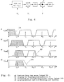
- FIG. 1 shows the basic circuit diagram of a digital AM residual sideband modulator according to the invention in the form of a double-balanced modulator M, which has the property of only generating the two sidebands without the original baseband video signal in the output spectrum.
- this digital mode of operation of a double push-pull modulator is shown schematically with a changeover switch S, with which the digital video signal supplied at the input E is alternately fed directly or inverted to the output A via an inverter J.
- the digital video signal is generated from the analog video signal in an A / D converter which is clocked at a sampling frequency f a or the digital video signal is directly generated in digital form at a sampling frequency f a and fed to the input E.
- the double push-pull modulator M is clocked at half the sampling frequency, ie its switch S is periodically switched between a and b in the cycle f a / 2, as is shown schematically in the switching scheme according to FIG. 1. From the relationship between the sampling of the video signal indicated schematically in Fig. 1 and this switching at half frequency of the switch S it follows that every second sample of the video signal is inverted, this corresponds to an amplitude modulation with the carrier frequency f a / 2 without this requires a correspondingly complex, digitally generated sine signal for the carrier, the modulation with the carrier is carried out only by switching the switch S. This results in a particularly simple structure. Theoretically, this mode of operation can be described by modulating the video signal with a carrier with half the sampling frequency. As a special feature, the two sidebands are symmetrical to the Nyquist frequency.
- FIG. 2 shows the implementation of this residual sideband filter with two low-pass filters TP1 and TP2
- FIG. 3 shows the associated diagram. That with the sampling frequency f a generated digital video signal u1 is fed to the low-pass filter TP1, which is also clocked at the sampling frequency f a .
- the filter characteristic of this low-pass filter TP1 is selected such that after the modulator M, in addition to the upper sideband, the frequency response of the lower sideband is also determined in a mirrored manner, as shown in FIG. 3b.
- the low-pass function of the low-pass filter TP1 is thus transformed into a high-pass characteristic.
- a second low-pass filter TP2 is arranged at the output of the modulator M and limits the upper sideband according to FIG. 3c in such a way that an asymmetrical residual sideband is produced.
- this second low-pass filter TP2 must act across the previous Nyquist frequency, a change in the sampling rate is necessary, for example a doubling of the sampling rate to 2f a .
- a circuit for inserting sample values of zero amplitude with the clock frequency 2f a is provided between the modulator M and the low pass filter TP2, so that virtually a data stream of twice the sampling frequency is produced.
- the low-pass filter TP2 can then be clocked at twice the sampling frequency 2f a .
- the double consideration of each sample value by repetition increases the power of the resulting signal, but in itself represents filtering that corresponds to a cosine-shaped frequency response with a single zero at the original sampling frequency f a .
- the second low-pass filter TP2 thus forms the upper sideband of the carrier-frequency video signal spectrum according to the video standard; together with the mirrored characteristic of the first low-pass filter TP1, a resulting bandpass results, the overall characteristics of which correspond to the prescribed residual sideband filter standard, the carrier frequency being f a / 2 (corresponds to the intermediate frequency 38.9 MHz of the residual sideband filter according to data sheet 341001). 3c with the carrier frequency f a / 2 is fed to a D / A converter according to FIG. 4 and disturbing harmonics are screened out via an analog low-pass filter TP3.
- the residual sideband signal according to FIG. 3d is generated with a relatively lower sampling frequency f a of only slightly more than twice the video bandwidth, it is also necessary to carry out an analog frequency conversion, for example to the standardized intermediate frequency of 38.9 MHz, according to Fig. 4, for example, with a mixer R, which is fed with a suitable carrier frequency F, a downstream bandpass filter BP1, the unused sidebands are filtered out.
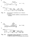
- FIG. 5 shows the implementation with an upstream low-pass filter TP1 according to FIG. 2, but with a high-pass filter HP arranged after the modulator M.
- the necessary for this Analog low-pass post-filter TP3 must be implemented with a steeper filter flank, since the first harmonic band is closer to the useful band.
- FIG. 6 and 7 show the implementation of the digital filter directly as a bandpass filter BP2.
- This direct implementation of the filter as a bandpass filter assumes that its clock frequency is clocked again at twice the sampling frequency 2f a .
- the characteristic of the analog pre-filter is also shown here in the form of a low-pass filter TP4.
- the spectral representation according to FIG. 7 shows that the analog prefilter TP4 may allow band overlaps, ie at the Nyquist frequency f a / 2 no very high blocking attenuation is required. This property applies analogously when two low-pass filters are used for RSB bandpass implementation.
- the sampling frequency f a must be chosen to be greater than twice the bandwidth (2 ⁇ 5 MHz) of the video signal, on the other hand it should be as small as possible for reasons of cheap implementation. If the sampling frequency were chosen to be 20 MHz, for example, which corresponds to a carrier frequency of 10 MHz, then a sampling frequency of 40 MHz would be required for the second low-pass filter TP2 or bandpass filter BP2, which is difficult to achieve in conventional TTL technology. For this reason it is advantageous to use a sampling frequency below 25 MHz.
- the first possibility is to select the sampling frequency f a in accordance with the sampling frequency of 13.5 MHz, which is defined for the digitization of video signals according to CCIR standard 601. This is the invention Modulator directly compatible with external digital studio devices, a digital video signal generated according to the standard can be fed directly at input E of the modulator, an additional A / D converter is unnecessary.
- the sampling frequency from other points of view, for example according to FIG. 8 such that the harmonic spectra arising during the modulation do not overlap the intended final carrier frequency spectrum after a final analog cooking mixture.
- the downstream D / A converter has a si-shaped post-filter effect, which normally has zeros in the sampling frequency and its multiples and which stands in the way of this advantageous utilization of the harmonics generated.
- Fig. 9 schematically shows this frequency response superimposed on the unevaluated scanning spectrum.
- This disruptive filter effect can be reduced by increasing the sampling frequency upstream of the D / A converter in conjunction with additionally inserted zero amplitudes between the actual sample values.This results in a pulse-amplitude-modulated output signal from a D / A converter with a smaller hold function, which has a weaker post-filter characteristic by shifting the zeros to higher frequencies, as shown in Figure 10.
- FIG. 12 shows how very advantageous frequency responses by increasing the clock frequency of the D.
- a purely digital modulator is to convert a COFDM-coded video signal present in the baseband from 0.4 to 8 MHz to the transmission frequency of an SFN transmitter, as is the case for processing the video signals in the individual transmitters of a single Frequency Network's is required.
- the COFDM-coded video signal which is supplied to all SFN transmitters, for example by a frequency-modulated satellite link, is digitally delayed via memory chains in a digital delay circuit, which operates with a sampling frequency f a of, for example, 20 MHz, and then in a modulator according to the invention with the aid of an intermediate frequency of, for example, 30 to 40 MHz is converted to the desired transmission frequency of the SFN transmitters.
- the corresponding time-delayed digital video signal with a carrier frequency of 10 MHz which is again half the sampling frequency f a in the delay circuit, is selected in the digital double push-pull modulator on the IF frequency implemented.
- the upper sideband between 30 and 40 MHz of the second repetition of the spectrum is filtered out as IF by digital filters. This can be done either by a bandpass with a 4-fold sampling frequency of 80 MHz or again by a low-pass filter with a sampling frequency of 20 MHz before the modulator and a low-pass filter with a 4-fold sampling frequency of 80 MHz after the modulator, as is shown in the previous figure is also described with respect to the residual sideband modulator.
- the IF signal is then converted to the actual transmission frequency of the SFN transmitter using a conventional analog mixer.
Landscapes
- Engineering & Computer Science (AREA)
- Signal Processing (AREA)
- Multimedia (AREA)
- Power Engineering (AREA)
- Computer Networks & Wireless Communication (AREA)
- Amplitude Modulation (AREA)
Applications Claiming Priority (2)
| Application Number | Priority Date | Filing Date | Title |
|---|---|---|---|
| DE4426935 | 1994-07-29 | ||
| DE19944426935 DE4426935A1 (de) | 1994-07-29 | 1994-07-29 | Digitaler Restseitenband-Modulator für Videosignale |
Publications (2)
| Publication Number | Publication Date |
|---|---|
| EP0695066A2 true EP0695066A2 (fr) | 1996-01-31 |
| EP0695066A3 EP0695066A3 (fr) | 1999-08-11 |
Family
ID=6524463
Family Applications (1)
| Application Number | Title | Priority Date | Filing Date |
|---|---|---|---|
| EP95108686A Withdrawn EP0695066A3 (fr) | 1994-07-29 | 1995-06-07 | Modulateur numérique pour des signaux vidéo |
Country Status (2)
| Country | Link |
|---|---|
| EP (1) | EP0695066A3 (fr) |
| DE (1) | DE4426935A1 (fr) |
Cited By (1)
| Publication number | Priority date | Publication date | Assignee | Title |
|---|---|---|---|---|
| EP0876077A3 (fr) * | 1997-04-18 | 2001-02-07 | Alcatel | Procédé et dispositif pour addition des signaux existants comme valeurs d'échangillons |
Families Citing this family (1)
| Publication number | Priority date | Publication date | Assignee | Title |
|---|---|---|---|---|
| DE102007001281B4 (de) | 2007-01-08 | 2018-10-18 | Rohde & Schwarz Gmbh & Co. Kg | Elektronisches Messgerät mit umschaltbarem Triggerfilter |
Family Cites Families (5)
| Publication number | Priority date | Publication date | Assignee | Title |
|---|---|---|---|---|
| GB1432373A (en) * | 1972-08-15 | 1976-04-14 | Indep Broadcasting Authority | Apparatus for producing digised signals for defining an amplitude modulated sub-carrier |
| NL168099C (nl) * | 1974-09-12 | 1982-02-16 | Philips Nv | Modulatie- en filterinrichting voor digitale signalen. |
| GB2219906A (en) * | 1988-06-15 | 1989-12-20 | Sony Corp | Image data transmitting systems |
| US4973977A (en) * | 1988-11-29 | 1990-11-27 | Comlux | Digital to amplitude modulated analog converter |
| FR2689350B1 (fr) * | 1992-03-30 | 1995-04-21 | France Telecom | Modulateur d'amplitude à bande latérale résiduelle pour signaux analogiques échantillonnés ou numériques et son utilisation en télévision. |
-
1994
- 1994-07-29 DE DE19944426935 patent/DE4426935A1/de not_active Withdrawn
-
1995
- 1995-06-07 EP EP95108686A patent/EP0695066A3/fr not_active Withdrawn
Non-Patent Citations (2)
| Title |
|---|
| MAEUSL: "Fernsehtechnik", HUETHIG BUCHVERLAG, HEIDELBERG, pages: 16 - 19 |
| SCHOENFELDER: "Nachrichrentechnik", JUSTUS VON LIEBIG VERLAG, DARMSTADT |
Cited By (2)
| Publication number | Priority date | Publication date | Assignee | Title |
|---|---|---|---|---|
| EP0876077A3 (fr) * | 1997-04-18 | 2001-02-07 | Alcatel | Procédé et dispositif pour addition des signaux existants comme valeurs d'échangillons |
| US6272181B1 (en) | 1997-04-18 | 2001-08-07 | Alcatel | Method and device for the aggregation of signals from sampling values |
Also Published As
| Publication number | Publication date |
|---|---|
| EP0695066A3 (fr) | 1999-08-11 |
| DE4426935A1 (de) | 1996-02-01 |
Similar Documents
| Publication | Publication Date | Title |
|---|---|---|
| DE69530214T2 (de) | Empfänger mit quadratur-dezimationsstufe und verfahren zur verarbeitung digitaler signale | |
| DE69107247T2 (de) | Elektronische Anordnung zum Empfangen eines modulierten Trägersignals. | |
| DE3786581T2 (de) | Kodierung und dekodierung von digitalen videokomponentensignalen. | |
| DE4337135C1 (de) | Drop-and-Add-Multiplexer zur Umsetzung und Aufbereitung eines Frequenzmultiplexsignals | |
| DE2703566B2 (de) | Frequenzmodulationssystem | |
| EP1657917B1 (fr) | Procédé et montage de circuit pour le filtrage de canal de signaux TV à modulation analogique ou numérique | |
| DE1816033B2 (de) | Sendevorrichtung zur uebertragung von impulsen | |
| EP0695066A2 (fr) | Modulateur numérique pour des signaux vidéo | |
| DE2608939C3 (de) | Mischer | |
| EP0651526A2 (fr) | Procédé de traitement d'un signal numérique à multiplexage de fréquence | |
| DE2730153A1 (de) | Verfahren und vorrichtung zum empfangen von radiosignalen nach dem ueberlagerungsprinzip | |
| DE2802938B2 (de) | Frequenzband-Teilungsfilter | |
| AT214988B (de) | Vorrichtung zur Umwandlung eines Farbfernsehsignals einer bestimmten Norm in ein Signal einer anderen Norm | |
| DE19731012B4 (de) | Anordnung zum Erzeugen eines restseitenband-modulierten Videosignals mit Restträger für einen Fernsehsender | |
| EP0834228A1 (fr) | Circuit de regulation de frequence et de phase pour recepteurs bla | |
| DE3922999C2 (de) | Tonzwischenfrequenz-Wandler | |
| EP0369102B1 (fr) | Procédé de modulation et montage pour réaliser le procédé | |
| WO2001015432A2 (fr) | Procede de conversion d'un signal d'image analogique module a valeur reelle et conversion correspondante dudit signal | |
| DE19628996A1 (de) | Schaltungsanordnung zur Frequenzumsetzung eines Farbsignals | |
| EP0109963B1 (fr) | Dispositif pour l'édition de porteuses d'image de signaux de télévision | |
| EP0632576B1 (fr) | Procédé de modulation de fréquence | |
| EP0631377A2 (fr) | Procédé de modulation de fréquence | |
| DE3918530A1 (de) | Modulator/demodulator, insbesondere fuer ein optisches kabelfernseh-uebertragungssystem | |
| DE2715834A1 (de) | Einseitenband-wellenerzeugungssystem | |
| DE3741610A1 (de) | Anordnung zur demodulation von einseitenbandsignalen |
Legal Events
| Date | Code | Title | Description |
|---|---|---|---|
| PUAI | Public reference made under article 153(3) epc to a published international application that has entered the european phase |
Free format text: ORIGINAL CODE: 0009012 |
|
| AK | Designated contracting states |
Kind code of ref document: A2 Designated state(s): DE FR GB IT |
|
| PUAL | Search report despatched |
Free format text: ORIGINAL CODE: 0009013 |
|
| AK | Designated contracting states |
Kind code of ref document: A3 Designated state(s): DE FR GB IT |
|
| RIC1 | Information provided on ipc code assigned before grant |
Free format text: 6H 04L 27/04 A, 6H 04N 7/24 B |
|
| 17P | Request for examination filed |
Effective date: 20000210 |
|
| STAA | Information on the status of an ep patent application or granted ep patent |
Free format text: STATUS: THE APPLICATION IS DEEMED TO BE WITHDRAWN |
|
| 18D | Application deemed to be withdrawn |
Effective date: 20030204 |