EP0696086B1 - Connecteur étanche pour carte de PC - Google Patents
Connecteur étanche pour carte de PC Download PDFInfo
- Publication number
- EP0696086B1 EP0696086B1 EP95111591A EP95111591A EP0696086B1 EP 0696086 B1 EP0696086 B1 EP 0696086B1 EP 95111591 A EP95111591 A EP 95111591A EP 95111591 A EP95111591 A EP 95111591A EP 0696086 B1 EP0696086 B1 EP 0696086B1
- Authority
- EP
- European Patent Office
- Prior art keywords
- terminal
- terminals
- housing
- receptacle connector
- stoppers
- Prior art date
- Legal status (The legal status is an assumption and is not a legal conclusion. Google has not performed a legal analysis and makes no representation as to the accuracy of the status listed.)
- Expired - Lifetime
Links
- 230000013011 mating Effects 0.000 claims description 9
- 239000004020 conductor Substances 0.000 claims description 5
- 239000000126 substance Substances 0.000 claims description 5
- 238000004519 manufacturing process Methods 0.000 claims description 3
- 238000000034 method Methods 0.000 claims description 3
- 239000002245 particle Substances 0.000 claims description 2
- 238000011109 contamination Methods 0.000 description 4
- 239000000356 contaminant Substances 0.000 description 3
- 238000003780 insertion Methods 0.000 description 1
- 230000037431 insertion Effects 0.000 description 1
- 238000005476 soldering Methods 0.000 description 1
Images




Classifications
-
- H—ELECTRICITY
- H01—ELECTRIC ELEMENTS
- H01R—ELECTRICALLY-CONDUCTIVE CONNECTIONS; STRUCTURAL ASSOCIATIONS OF A PLURALITY OF MUTUALLY-INSULATED ELECTRICAL CONNECTING ELEMENTS; COUPLING DEVICES; CURRENT COLLECTORS
- H01R12/00—Structural associations of a plurality of mutually-insulated electrical connecting elements, specially adapted for printed circuits, e.g. printed circuit boards [PCB], flat or ribbon cables, or like generally planar structures, e.g. terminal strips, terminal blocks; Coupling devices specially adapted for printed circuits, flat or ribbon cables, or like generally planar structures; Terminals specially adapted for contact with, or insertion into, printed circuits, flat or ribbon cables, or like generally planar structures
- H01R12/50—Fixed connections
- H01R12/51—Fixed connections for rigid printed circuits or like structures
- H01R12/55—Fixed connections for rigid printed circuits or like structures characterised by the terminals
-
- H—ELECTRICITY
- H01—ELECTRIC ELEMENTS
- H01R—ELECTRICALLY-CONDUCTIVE CONNECTIONS; STRUCTURAL ASSOCIATIONS OF A PLURALITY OF MUTUALLY-INSULATED ELECTRICAL CONNECTING ELEMENTS; COUPLING DEVICES; CURRENT COLLECTORS
- H01R13/00—Details of coupling devices of the kinds covered by groups H01R12/70 or H01R24/00 - H01R33/00
- H01R13/46—Bases; Cases
- H01R13/52—Dustproof, splashproof, drip-proof, waterproof, or flameproof cases
- H01R13/5205—Sealing means between cable and housing, e.g. grommet
- H01R13/5208—Sealing means between cable and housing, e.g. grommet having at least two cable receiving openings
-
- H—ELECTRICITY
- H01—ELECTRIC ELEMENTS
- H01R—ELECTRICALLY-CONDUCTIVE CONNECTIONS; STRUCTURAL ASSOCIATIONS OF A PLURALITY OF MUTUALLY-INSULATED ELECTRICAL CONNECTING ELEMENTS; COUPLING DEVICES; CURRENT COLLECTORS
- H01R13/00—Details of coupling devices of the kinds covered by groups H01R12/70 or H01R24/00 - H01R33/00
- H01R13/40—Securing contact members in or to a base or case; Insulating of contact members
- H01R13/42—Securing in a demountable manner
-
- H—ELECTRICITY
- H01—ELECTRIC ELEMENTS
- H01R—ELECTRICALLY-CONDUCTIVE CONNECTIONS; STRUCTURAL ASSOCIATIONS OF A PLURALITY OF MUTUALLY-INSULATED ELECTRICAL CONNECTING ELEMENTS; COUPLING DEVICES; CURRENT COLLECTORS
- H01R13/00—Details of coupling devices of the kinds covered by groups H01R12/70 or H01R24/00 - H01R33/00
- H01R13/62—Means for facilitating engagement or disengagement of coupling parts or for holding them in engagement
- H01R13/627—Snap or like fastening
-
- H—ELECTRICITY
- H01—ELECTRIC ELEMENTS
- H01R—ELECTRICALLY-CONDUCTIVE CONNECTIONS; STRUCTURAL ASSOCIATIONS OF A PLURALITY OF MUTUALLY-INSULATED ELECTRICAL CONNECTING ELEMENTS; COUPLING DEVICES; CURRENT COLLECTORS
- H01R12/00—Structural associations of a plurality of mutually-insulated electrical connecting elements, specially adapted for printed circuits, e.g. printed circuit boards [PCB], flat or ribbon cables, or like generally planar structures, e.g. terminal strips, terminal blocks; Coupling devices specially adapted for printed circuits, flat or ribbon cables, or like generally planar structures; Terminals specially adapted for contact with, or insertion into, printed circuits, flat or ribbon cables, or like generally planar structures
- H01R12/70—Coupling devices
- H01R12/71—Coupling devices for rigid printing circuits or like structures
- H01R12/72—Coupling devices for rigid printing circuits or like structures coupling with the edge of the rigid printed circuits or like structures
- H01R12/721—Coupling devices for rigid printing circuits or like structures coupling with the edge of the rigid printed circuits or like structures cooperating directly with the edge of the rigid printed circuits
Definitions
- the present invention relates to an electrical connector, and more particularly, to a receptacle connector for an IC card.
- FIG. 15 shows a conventional receptacle connector in an assembled IC card 54.
- receptacle terminals 52 are press-fit in terminal-receiving cavities 53 of a housing 51.
- cover members 58 seal and protect the internal circuit board 56 of the IC card from contaminants and other foreign substances, some moisture and other small size foreign substances may enter the IC card 54 via the cavities 53, as indicated by arrows 55. Therefore there is a potential for contamination of or damage to the integrated circuitry 57 on the surface of internal circuit board 56 of the IC card.
- the portable nature of IC cards and the removal of the cards from relatively clean areas such as offices further increases the likelihood of the ingress of foreign substances into the IC card.
- housing 51 and terminals 52 are integrally or unitarily formed, such as in a single overmolding process to eliminate cavities 53.
- the receptacle connector would then be sealed to the environment except for the smaller inlet apertures 61 at the front mating edge thereof, which receive the contact pins of a mating connector (not shown).
- An object of the present invention is to provide a sealed receptacle connector for an IC card, which receptacle connector prevents the ingress of foreign contaminants into the IC card, and which does not add significantly to the cost of manufacturing and assembling such receptacle connectors.
- a receptacle connector which includes an insulative housing, a plurality of inlet apertures at a first end of the housing for receiving contacts of a mating connector, the inlet apertures communicating with terminal-receiving cavities extending rearwardly therefrom, and a corresponding plurality of receptacle terminals inserted in the cavities.
- Each of the plurality of receptacle terminals is connected to an insulative stopper, and each stopper is adapted to be press-fit within the housing at a second end thereof, whereby, when the terminals and stoppers are inserted in the terminal-receiving cavities, the cavities are sealed from the environment by the stoppers.
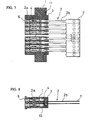
- the receptacle connector comprises an elongated insulative housing 1, a plurality of receptacle terminals 2 and a corresponding plurality of stoppers 3.
- the housing 1 is composed of an upper and a lower row of terminal-receiving cavities 4.
- the terminals 2a are inserted in the upper and lower terminal-receiving cavities 4 of the housing 1 and are adapted to be connected to electronic circuitry (not shown) formed on opposite surfaces of a circuit board 5 of an IC card, thereby permitting the circuitry of the circuit board to be connected to mating contact pins (not shown) when the contact pins are received through inlet apertures 6 of housing 1.
- the receptacle connector is adapted to be fixed to one end of the circuit board, as shown in Figure 2.
- the terminal-receiving cavities 4 are sealed at their ends by stoppers 3, thereby preventing the ingress of foreign substances into the IC card through the inlet apertures and the terminal-receiving cavities, and preventing contamination of the internal circuitry of the circuit board.
- terminals 2 are shown prior to assembly of the receptacle connector.
- the terminals 2 are arranged at a given spacing and connected by a carrier strip 7.
- Each terminal includes a terminal contact 2a at an end opposite the carrier strip, and a conductor extension 2b which extends between the terminal contact 2a and the carrier strip 7.
- Guide pieces 8 are arranged between adjacent conductor extensions 2b, and also extend from carrier strip 7.
- terminal contacts 2a are arranged at predetermined spacing, for example at intervals of 1.0 mm.
- the terminals are then insert-molded with the stoppers to form a unitary terminal-and-stopper assembly.
- terminal-and-stopper assembly is then press-fit into housing 1 from the rear end thereof by inserting terminal contacts 2a into terminal-receiving cavities 4 so that the stoppers are press-fit within a recess or opening 11 of housing 1, as shown in Figures 5 and 6.
- the fully assembled receptacle is shown in Figures 7 and 8.
- the cavities 4 of housing 1 are completely sealed by the stopper 3, which otherwise would permit foreign contaminants into the IC card by way of the terminal-receiving cavities and expose the circuitry of the printed circuit board thereto.
- the carrier strip 7 is then cut and removed from the conductive extensions 2b, and then, as shown in Figure 2, the free ends of the conductive extensions 2b are formed divergently to facilitate the insertion of the circuit board 5 between the rows of terminals 2 and the soldering of the free ends of the extensions 2b to the surface of the circuit board.
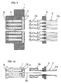
- terminals 2 and associated stoppers 3 are insert-molded to form a single terminal-and-stopper assembly.
- the terminals 2 are simply press-fit within an associated stopper member 3 to provide the unitary terminal-and-stopper assembly.
- the terminal-and-stopper assembly is then press-fit into housing 1 from the rear end thereof, as indicated by arrow 20 in Figure 10, until stopper 3 is positively fixed or press-fit into recess 11 of housing 1, to provide the receptacle assembly as shown in Figures 11 and 12.
- a receptacle connector is described according to a third embodiment of the invention.
- the receptacle connector is adapted to be fixed to the end of the circuit board 5 (Fig. 2), but in the third embodiment the receptacle is fixed to the surface of a circuit board 5 (Fig. 14(c)).
- terminals 2 and associated stopper 3 are integrally connected by either method described above, and then, as shown in Figures 14a and 14b, the terminal-and-stopper assembly is assembled within housing 1.
- the receptacle is then adapted to be fixed to the surface of the circuit board 5 of an IC card as shown in Figure 14c.
- Mating contact pins are adapted to be inserted into the receptacle in a direction transverse to the surface of circuit board 5.
- a receptacle connector includes a housing whose terminal-receiving cavities are each sealed by a stopper to prevent the ingress of foreign particles therethrough and to avoid the potential contamination of and/or damage to the circuitry of the internal circuit board of an IC card in which the receptacle connector is assembled.
Landscapes
- Connector Housings Or Holding Contact Members (AREA)
- Coupling Device And Connection With Printed Circuit (AREA)
- Manufacturing Of Electrical Connectors (AREA)
Claims (7)
- Connecteur femelle pour un dispositif à circuit intégré comprenant :un boîtier allongé (1) comportant plusieurs cavités de réception de borne (4) s'étendant à travers celui-ci, et plusieurs ouvertures d'entrée (6) formées à une première extrémité du boîtier et étant en communication avec les cavités de réception de borne pour recevoir des broches de contact d'un connecteur complémentaire ;plusieurs bornes (2) situées dans les cavités de réception de borne (4) pour être connectées électriquement aux broches de contact du connecteur complémentaire ;plusieurs pièces d'arrêt (3), chacune étant fixée à l'une correspondante des plusieurs bornes (2), dans lequel chaque pièce d'arrêt est introduite à force dans le boîtier à sa seconde extrémité, ce par quoi chaque cavité de réception de borne est rendue étanche par l'une des pièces d'arrêt pour empêcher l'entrée, par celle-ci, de particules étrangères.
- Connecteur femelle selon la revendication 1, dans lequel les cavités de réception de borne du boîtier allongé et les bornes y sont agencées en deux rangées.
- Connecteur femelle selon la revendication 1, dans lequel les plusieurs pièce d'arrêt sont formées dans un élément d'une seule pièce qui s'ajuste dans un évidement (11) du boîtier allongé.
- Connecteur femelle selon la revendication 1, dans lequel les bornes sont introduites à force dans les pièces d'arrêt pour former un ensemble bornes et pièces d'arrêt unique, et dans lequel les pièces d'arrêt retiennent les bornes dans leur position correcte à l'intérieur du boîtier.
- Connecteur femelle selon la revendication 2, dans lequel les deux rangées de bornes sont définies par une rangée supérieure de bornes et par une rangée inférieure de bornes qui sont aptes à chevaucher une carte à circuit imprimé (5) du dispositif à circuit intégré.
- Connecteur femelle selon la revendication 1, dans lequel chaque borne comprend un contact de borne (2a) à son extrémité et un prolongement conducteur (2b) qui s'étend depuis le contact de borne, dans lequel la pièce d'arrêt respective est située le long du prolongement conducteur (2b) à proximité de la jonction entre le contact de borne et le prolongement conducteur.
- Procédé de fabrication d'un connecteur femelle pour un dispositif à circuit intégré, le connecteur femelle comprenant un boîtier allongé (1) comportant plusieurs cavités de réception de borne (4) s'étendant à travers celui-ci, plusieurs bornes (2) sous forme d'une bande de bornes et aptes à se placer dans les cavités de réception de borne (4). plusieurs pièces d'arrêt (3) correspondant chacune à l'une des plusieurs bornes et étant apte à être introduite à force dans le boîtier, le procédé comprenant les étapes :a) de surmoulage de la bande de bornes sur les pièces d'arrêt pour fournir un ensemble bornes et pièces d'arrêt d'un seul tenant ;b) d'introduction de l'ensemble bornes et pièces d'arrêt dans le boîtier, de sorte que chacune des plusieurs bornes est placée dans une cavité de réception de borne correspondante ; etc) de fixation des pièces d'arrêt dans un évidement du boîtier dans lequel les bornes sont correctement placées à l'intérieur du boîtier pour recevoir les broches d'accouplement d'un connecteur complémentaire, et dans lequel les cavités de réception de borne sont chacune rendues étanches à une extrémité par une pièce d'arrêt correspondante pour empêcher l'entrée, par celles-ci, de substances étrangères.
Applications Claiming Priority (2)
| Application Number | Priority Date | Filing Date | Title |
|---|---|---|---|
| JP6200200A JPH0864315A (ja) | 1994-08-02 | 1994-08-02 | リセプタクル型電気コネクタ |
| JP200200/94 | 1994-08-02 |
Publications (2)
| Publication Number | Publication Date |
|---|---|
| EP0696086A1 EP0696086A1 (fr) | 1996-02-07 |
| EP0696086B1 true EP0696086B1 (fr) | 1997-09-10 |
Family
ID=16420471
Family Applications (1)
| Application Number | Title | Priority Date | Filing Date |
|---|---|---|---|
| EP95111591A Expired - Lifetime EP0696086B1 (fr) | 1994-08-02 | 1995-07-24 | Connecteur étanche pour carte de PC |
Country Status (6)
| Country | Link |
|---|---|
| US (1) | US5597324A (fr) |
| EP (1) | EP0696086B1 (fr) |
| JP (1) | JPH0864315A (fr) |
| KR (1) | KR200146617Y1 (fr) |
| CN (1) | CN1120748A (fr) |
| DE (1) | DE69500689T2 (fr) |
Families Citing this family (17)
| Publication number | Priority date | Publication date | Assignee | Title |
|---|---|---|---|---|
| AU708668B2 (en) * | 1997-11-21 | 1999-08-12 | Xybernaut Corporation | A computer structure for accommodating a PC card |
| US6000975A (en) * | 1997-12-12 | 1999-12-14 | 3M Innovative Properties Company | Canted beam electrical contact and receptacle housing therefor |
| US6453552B1 (en) * | 1998-01-30 | 2002-09-24 | Molex Incorporated | Method of manufacturing electrical terminals and terminal modules |
| US6152781A (en) * | 1999-08-12 | 2000-11-28 | Hon Hai Precisdion Ind. Co., Ltd. | Electrical connector |
| US6409541B1 (en) | 2000-11-02 | 2002-06-25 | Autonetworks Technologies, Ltd. | Waterproof structure in cable insertion section, method of manufacturing the same, and die for waterproof molding |
| US6402552B1 (en) | 2001-08-07 | 2002-06-11 | Fci Americas Technology, Inc. | Electrical connector with overmolded and snap locked pieces |
| JP2005019321A (ja) * | 2003-06-27 | 2005-01-20 | Auto Network Gijutsu Kenkyusho:Kk | コネクタ及びコネクタの製造方法 |
| US8033868B2 (en) * | 2008-08-27 | 2011-10-11 | Hon Hai Precision Ind. Co., Ltd. | Electrical connector with a tongue |
| DE102011051644B4 (de) * | 2011-07-07 | 2014-11-13 | Amphenol-Tuchel Electronics Gmbh | Schnittstellenstecker |
| JP5391308B2 (ja) * | 2012-05-17 | 2014-01-15 | 日本航空電子工業株式会社 | 防水コネクタ |
| JP6005448B2 (ja) * | 2012-09-04 | 2016-10-12 | 日本航空電子工業株式会社 | 防水コネクタ |
| US9847597B2 (en) | 2013-10-03 | 2017-12-19 | Molex, Llc | Electrical connector with sealing structure |
| CN104795657B (zh) * | 2014-01-16 | 2017-07-11 | 凡甲电子(苏州)有限公司 | 充电电池插座 |
| DE102014223644A1 (de) * | 2014-11-19 | 2016-05-19 | Zf Friedrichshafen Ag | Steckeranordnung mit zumindest einem Steckerelement |
| JP6534370B2 (ja) * | 2016-08-29 | 2019-06-26 | 矢崎総業株式会社 | ピン端子及びコネクタ |
| US9877404B1 (en) * | 2017-01-27 | 2018-01-23 | Ironwood Electronics, Inc. | Adapter apparatus with socket contacts held in openings by holding structures |
| DE102021105218A1 (de) | 2021-03-04 | 2022-09-08 | Marquardt Gmbh | Schaltmodul ausgebildet mit einer abgedichteten Schnittstelle |
Family Cites Families (10)
| Publication number | Priority date | Publication date | Assignee | Title |
|---|---|---|---|---|
| JPS5322748Y2 (fr) * | 1972-04-13 | 1978-06-13 | ||
| DE3884708T2 (de) * | 1987-07-28 | 1994-05-05 | Whitaker Corp | Leitungsersatzsteckverbindungszusammenbau für Verwendung mit gedruckten Schaltungskarten. |
| US4808115A (en) * | 1987-07-28 | 1989-02-28 | Amp Incorporated | Line replaceable connector assembly for use with printed circuit boards |
| US4776813A (en) * | 1987-12-08 | 1988-10-11 | Molex Incorporated | Sealed connector assembly |
| FR2641135A1 (en) * | 1988-12-23 | 1990-06-29 | Thomson Csf | Method of manufacturing a sealed connector and connector obtained by this method |
| JPH02204980A (ja) * | 1989-01-25 | 1990-08-14 | Thomas & Betts Corp <T&B> | コネクタ |
| US4981446A (en) * | 1989-11-06 | 1991-01-01 | The Boeing Company | Modular, circular, environment resistant electrical connector assembly |
| US5145410A (en) * | 1990-08-06 | 1992-09-08 | Yazaki Corporation | Waterproof connector |
| JP2505387Y2 (ja) * | 1991-02-12 | 1996-07-31 | 矢崎総業株式会社 | 端子金具と防水栓の固定構造 |
| US5266045A (en) * | 1991-10-28 | 1993-11-30 | Yazaki Corporation | Waterproof connector |
-
1994
- 1994-08-02 JP JP6200200A patent/JPH0864315A/ja active Pending
-
1995
- 1995-06-30 US US08/497,011 patent/US5597324A/en not_active Expired - Fee Related
- 1995-07-24 DE DE69500689T patent/DE69500689T2/de not_active Expired - Fee Related
- 1995-07-24 EP EP95111591A patent/EP0696086B1/fr not_active Expired - Lifetime
- 1995-08-01 KR KR2019950019879U patent/KR200146617Y1/ko not_active Expired - Fee Related
- 1995-08-01 CN CN95109334A patent/CN1120748A/zh active Pending
Also Published As
| Publication number | Publication date |
|---|---|
| CN1120748A (zh) | 1996-04-17 |
| JPH0864315A (ja) | 1996-03-08 |
| KR960009316U (ko) | 1996-03-16 |
| KR200146617Y1 (ko) | 1999-06-15 |
| DE69500689D1 (de) | 1997-10-16 |
| US5597324A (en) | 1997-01-28 |
| DE69500689T2 (de) | 1998-03-12 |
| EP0696086A1 (fr) | 1996-02-07 |
Similar Documents
| Publication | Publication Date | Title |
|---|---|---|
| EP0696086B1 (fr) | Connecteur étanche pour carte de PC | |
| US4274700A (en) | Low cost electrical connector | |
| US5702258A (en) | Electrical connector assembled from wafers | |
| EP0772898B1 (fr) | Enveloppe de protection de mise a la terre amelioree pour connecteurs electriques | |
| US6071152A (en) | Electrical connector with inserted terminals | |
| US7198519B2 (en) | Edge card connector assembly with keying means for ensuring proper connection | |
| US6231355B1 (en) | Matched impedance connector having retention device on a grounding plane | |
| EP0633631B1 (fr) | Connecteur électrique de bord pour une plaquette à circuits imprimés | |
| KR100248966B1 (ko) | 감지 단자 시스템을 구비한 전기 커넥터 | |
| US6592407B2 (en) | High-speed card edge connector | |
| US5281165A (en) | Electrical connector shroud adapted for shorting bar removal | |
| US6022245A (en) | Filtered modular connector | |
| US6371790B1 (en) | Electrical assembly having anti-mismating device | |
| US6688909B1 (en) | Stacked connector with leds | |
| US5997312A (en) | Grounding contact for high speed, high density connector | |
| US6645009B1 (en) | High density electrical connector with lead-in device | |
| US20040053540A1 (en) | Electrical connector and method of assembling the same | |
| US20030166347A1 (en) | Low-profile connector for circuit boards | |
| US6508665B1 (en) | Electrical connector having printed circuit board mounted therein | |
| US20080009195A1 (en) | Electrical interconnection with mating terminals | |
| EP0932226A2 (fr) | Connecteur pour carte | |
| CA1101953A (fr) | Traduction non-disponible | |
| US6152781A (en) | Electrical connector | |
| US7367818B2 (en) | Onboard connector | |
| CN1983732A (zh) | 带有电线管理系统的电气连接器 |
Legal Events
| Date | Code | Title | Description |
|---|---|---|---|
| PUAI | Public reference made under article 153(3) epc to a published international application that has entered the european phase |
Free format text: ORIGINAL CODE: 0009012 |
|
| AK | Designated contracting states |
Kind code of ref document: A1 Designated state(s): DE FR GB IT NL |
|
| 17P | Request for examination filed |
Effective date: 19960724 |
|
| GRAG | Despatch of communication of intention to grant |
Free format text: ORIGINAL CODE: EPIDOS AGRA |
|
| 17Q | First examination report despatched |
Effective date: 19961217 |
|
| GRAH | Despatch of communication of intention to grant a patent |
Free format text: ORIGINAL CODE: EPIDOS IGRA |
|
| ITF | It: translation for a ep patent filed | ||
| GRAH | Despatch of communication of intention to grant a patent |
Free format text: ORIGINAL CODE: EPIDOS IGRA |
|
| GRAA | (expected) grant |
Free format text: ORIGINAL CODE: 0009210 |
|
| AK | Designated contracting states |
Kind code of ref document: B1 Designated state(s): DE FR GB IT NL |
|
| REF | Corresponds to: |
Ref document number: 69500689 Country of ref document: DE Date of ref document: 19971016 |
|
| ET | Fr: translation filed | ||
| PLBE | No opposition filed within time limit |
Free format text: ORIGINAL CODE: 0009261 |
|
| STAA | Information on the status of an ep patent application or granted ep patent |
Free format text: STATUS: NO OPPOSITION FILED WITHIN TIME LIMIT |
|
| 26N | No opposition filed | ||
| PGFP | Annual fee paid to national office [announced via postgrant information from national office to epo] |
Ref country code: GB Payment date: 20000614 Year of fee payment: 6 |
|
| PGFP | Annual fee paid to national office [announced via postgrant information from national office to epo] |
Ref country code: NL Payment date: 20000620 Year of fee payment: 6 |
|
| PGFP | Annual fee paid to national office [announced via postgrant information from national office to epo] |
Ref country code: FR Payment date: 20000707 Year of fee payment: 6 |
|
| PGFP | Annual fee paid to national office [announced via postgrant information from national office to epo] |
Ref country code: DE Payment date: 20000727 Year of fee payment: 6 |
|
| PG25 | Lapsed in a contracting state [announced via postgrant information from national office to epo] |
Ref country code: GB Free format text: LAPSE BECAUSE OF NON-PAYMENT OF DUE FEES Effective date: 20010724 |
|
| PG25 | Lapsed in a contracting state [announced via postgrant information from national office to epo] |
Ref country code: NL Free format text: LAPSE BECAUSE OF NON-PAYMENT OF DUE FEES Effective date: 20020201 |
|
| GBPC | Gb: european patent ceased through non-payment of renewal fee |
Effective date: 20010724 |
|
| PG25 | Lapsed in a contracting state [announced via postgrant information from national office to epo] |
Ref country code: FR Free format text: LAPSE BECAUSE OF NON-PAYMENT OF DUE FEES Effective date: 20020329 |
|
| NLV4 | Nl: lapsed or anulled due to non-payment of the annual fee |
Effective date: 20020201 |
|
| PG25 | Lapsed in a contracting state [announced via postgrant information from national office to epo] |
Ref country code: DE Free format text: LAPSE BECAUSE OF NON-PAYMENT OF DUE FEES Effective date: 20020501 |
|
| REG | Reference to a national code |
Ref country code: FR Ref legal event code: ST |
|
| PG25 | Lapsed in a contracting state [announced via postgrant information from national office to epo] |
Ref country code: IT Free format text: LAPSE BECAUSE OF NON-PAYMENT OF DUE FEES;WARNING: LAPSES OF ITALIAN PATENTS WITH EFFECTIVE DATE BEFORE 2007 MAY HAVE OCCURRED AT ANY TIME BEFORE 2007. THE CORRECT EFFECTIVE DATE MAY BE DIFFERENT FROM THE ONE RECORDED. Effective date: 20050724 |