EP0696106A1 - Convertisseur a/n - Google Patents
Convertisseur a/n Download PDFInfo
- Publication number
- EP0696106A1 EP0696106A1 EP95907824A EP95907824A EP0696106A1 EP 0696106 A1 EP0696106 A1 EP 0696106A1 EP 95907824 A EP95907824 A EP 95907824A EP 95907824 A EP95907824 A EP 95907824A EP 0696106 A1 EP0696106 A1 EP 0696106A1
- Authority
- EP
- European Patent Office
- Prior art keywords
- phase
- analogue
- output
- signal
- aforementioned
- Prior art date
- Legal status (The legal status is an assumption and is not a legal conclusion. Google has not performed a legal analysis and makes no representation as to the accuracy of the status listed.)
- Ceased
Links
Images


Classifications
-
- H—ELECTRICITY
- H03—ELECTRONIC CIRCUITRY
- H03M—CODING; DECODING; CODE CONVERSION IN GENERAL
- H03M1/00—Analogue/digital conversion; Digital/analogue conversion
- H03M1/12—Analogue/digital converters
- H03M1/64—Analogue/digital converters with intermediate conversion to phase of sinusoidal or similar periodical signals
-
- H—ELECTRICITY
- H03—ELECTRONIC CIRCUITRY
- H03M—CODING; DECODING; CODE CONVERSION IN GENERAL
- H03M1/00—Analogue/digital conversion; Digital/analogue conversion
- H03M1/12—Analogue/digital converters
- H03M1/34—Analogue value compared with reference values
- H03M1/36—Analogue value compared with reference values simultaneously only, i.e. parallel type
- H03M1/368—Analogue value compared with reference values simultaneously only, i.e. parallel type having a single comparator per bit, e.g. of the folding type
Definitions
- This invention is utilized as an element of an electronic circuit, and for high-speed analogue-to-digital conversion. It is suitable for use in sampling oscilloscopes and LSI testers, and relates in particular to technology for improving the conversion precision and sensitivity of ultrahigh-speed analogue-to-digital converters.
- Fig.19 shows a conventional ultrahigh-speed analogue-to-digital converter.
- Fig.19(a) shows a known circuit for performing ultrahigh-speed analogue-to-digital conversion: namely, an analogue-to-digital converter which changes the phase of light in accordance with the electric field strength of an analogue input, and which employs a Mach-Zehnder interferometer to convert this to optical intensity by means of interference.
- Analogue-to-digital conversion is achieved by applying binary weighting to the phase changes (see "Novel GaAs/AlGaAs Guided-Wave Analogue/Digital Convertor", R.G. Walker et al., Electronics Letters , 12th October 1989, Vol.25, No.21, pp.1443-1444).
- Fig.19(b) shows an implementation of this analogue-to-digital converter.
- analogue-to-digital converter employing a Mach-Zehnder interferometer
- noise from the optical source, and phase noise in particular is large compared with the signal obtained by the electrical means, and the conversion efficiency of Mach-Zehnder interferometers and other electro-optic converters is low, so that a large-amplitude analogue input signal is required in order to obtain adequate signal strength.
- it is necessary to lengthen the interferometer which means that a large analogue-to-digital converter becomes necessary.
- a large signal input will still be required to drive such a large interferometer.
- the present invention has been designed in the light of this situation. It is an object of this invention to improve the precision and accuracy of analogue-to-digital converters and to enable them to operate at higher frequencies. It is a further object of this invention to provide an ultrahigh-speed analogue-to-digital converter which has high sensitivity. Finally, it is another object of this invention to provide an analogue-to-digital converter which can achieve high resolution analogue-to-digital conversion by means of a simple circuit configuration.
- this invention is characterised in that, despite offering ultrahigh-speed conversion, high signal quality is ensured and efficient conversion performed by means of electric signals alone, without using optical signals.
- this invention is an analogue-to-digital converter which is characterised in that it has an analogue signal input terminal, a carrier generator, and a plural number n of phase modulators which respectively phase modulate this carrier with the analogue signal; and the modulation factor of the i th modulator of these n phase modulators ( i ⁇ n ) is: ⁇ ⁇ 2 i -1 where ⁇ is a constant; and it has n phase comparators which respectively compare the phase of the output of these n phase modulators with the phase of the aforementioned carrier, and n digital output terminals from which the output of these phase comparators is respectively sent.
- the aforementioned i th phase modulator can also be constituted from phase modulating elements with modulation factor ⁇ cascade-connected in 2 i-1 stages.
- An alternative configuration is for at least some of the plurality of cascade-connected phase modulating elements to be shared by the plurality of phase modulators.
- the phase of the carrier is modulated in proportion to the analogue signal, and analogue-to-digital conversion is performed by using the periodicity of the phase modulation (i.e., the phase of the output cycles between 0 and 2 ⁇ radians as the strength of the modulating signal increases). That is to say, the modulated signal and the carrier are both input to a phase comparator.
- the output of the phase comparator is made logical level "L” when the phase difference between the modulated wave and the carrier is within the range 0 ⁇ (1/2) ⁇ radians, and is made logical level "H” when said phase difference is within the range ⁇ (1/2) ⁇ radians.
- the output of the phase comparator will be “L” for analogue inputs from “0" to 1/2 full scale, and “H” for analogue inputs from 1/2 full scale to full scale. Because the modulation factor for the bit in the next position is doubled, the phase comparator output will be “L” for analogue inputs from “0” to 1/4 full scale, “H” for analogue inputs from 1/4 full scale to 3/4 full scale, and “L” again from 3/4 full scale to full scale. Conversion to successive digital signals is carried out in this way down to the least significant bit, thereby converting the analogue signal to a digital signal in positive logic Gray code.
- the number of phase modulators provided for forming modulated signals has to be the same as the number of bits, and their modulation factor has to double with every move from the most significant bit towards the least significant bit.
- a modulation factor of n ⁇ can be obtained by, for example, connecting a plurality of phase modulating elements with modulation factor ⁇ in series, whereupon this ⁇ is multiplied by the number of connected stages n .
- the desired modulation factor can be obtained by establishing a suitable number of connected stages.
- An ultrahigh-speed analogue-to-digital converter with high precision, accuracy and sensitivity can be achieved in this manner.
- this invention has an analogue signal input terminal, a carrier generator, and a first phase modulating element which phase modulates this carrier with the analogue signal; and 2 n -1 delay elements are provided in the output path of the aforementioned carrier or in the output path of the aforementioned first phase modulating element, said delay elements applying, in 2 n -1 stages (where n is the resolution), different relative delays between the aforementioned carrier and the output signal from the aforementioned first phase modulating element; and the relative delay time of the i th delay element of these 2 n -1 delay elements ( i ⁇ n ) is set to: ( i -1) ⁇ T /(2 n 1 ) where T is the carrier period; and there are also provided 2 n -1 first phase comparators which compare the phase of the signal which has passed through these delay elements with the phase of either the aforementioned carrier output or the aforementioned first phase modulating element output, which have not passed through these delay elements; and a logic gate to which are input the outputs of
- the aforementioned delay elements prefferably be inserted in approximately equal numbers on the output path side of the aforementioned carrier and on the output path side of the aforementioned first phase modulating element.
- the carrier should be a sine wave.
- the aforementioned delay elements can also be constituted from delay elements with unit delay times of T/2 n + 1 cascade-connected in a plurality of stages.
- this invention has the analogue-to-digital converter explained in the earlier part of this section and the analogue-to-digital converter explained in the latter part of this section; and in respect of a common analogue signal input, the output of the analogue-to-digital converter explained in the earlier part constitutes the more significant bits, and the output of the analogue-to-digital converter explained in the latter part constitutes the less significant bits.
- high-resolution analogue-to-digital conversion can be achieved by means of simple circuit configurations, and high-speed analogue-to-digital conversion can be performed.
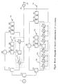
- Fig.1 is a block diagram of said first embodiment.
- This invention is an analogue-to-digital converter, and its distinguishing features are that it has analogue signal input terminal 10, sine wave source 1 as the carrier generator, and a plural number n of phase modulators P1-Pn which respectively phase modulate this sine wave signal with the analogue signal; and the modulation factor of the i th phase modulator Pi of these n phase modulators P1 ⁇ Pn is: 2 i 1 ⁇ ⁇ radians and it has n phase comparators 41 ⁇ 4n which respectively compare the phase of the output of these n phase modulators P1 ⁇ Pn with the phase of the sine wave signal, and n digital signal output terminals 71 ⁇ 7n from which the output of these phase comparators 41 ⁇ 4n is sent.
- the number of phase modulators P1 ⁇ Pn and phase comparators 41 ⁇ 4n provided is equal to the number of bits n of the digital signal that is output; and if the aforementioned modulation factor of phase modulator P1 corresponding to the position of the most significant bit (MSB) is made ⁇ radians, the modulation factor of phase modulator Pn corresponding to the position of the n th bit from the MSB will be 2 n-1 ⁇ radians.
- phase modulators P1 ⁇ Pn The output from sine wave source 1 is supplied to phase modulators P1 ⁇ Pn, the number of which is the same as the resolution ( n bits).
- the phase of these inputs is modulated in proportion to the analogue signal that is input from analogue signal input terminal 10. Relative to the full scale of the input, the modulation factor of phase modulating elements 31 ⁇ 3n in phase modulators P1 ⁇ Pn doubles from one phase modulator to the next, being 0 ⁇ radians in the case of phase modulating element 31 and 0 ⁇ 2 ⁇ radians in the case of phase modulating element 32.
- the outputs of phase modulators P1 ⁇ Pn are compared with the phase of the original sine wave by means of phase comparators 41 ⁇ 4n. As shown in Fig. 12 , the output of phase comparators 41 ⁇ 4n is made "L” when the phase difference is 0 ⁇ (1/2) ⁇ radians, and "H" when the phase difference is ⁇ (1/2) ⁇ radians.
- phase comparator 41 In the case of the MSB, because the modulation factor of phase modulator P1 is ⁇ radians, the output of phase comparator 41 will be “L” for analogue inputs of up to 1/2 full scale, and "H” when this is exceeded.
- phase comparator 42 Because the next bit after the MSB will have a modulation factor of twice this, i.e., 2 ⁇ radians, the output of phase comparator 42 will change from “L” to "H” at 1/4 full scale analogue input and will then return to "L” at 3/4 full scale.
- phasecomparators 41 ⁇ 4n doubles with every move to a less significant bit.
- Fig.2 shows the relation between analogue signal strength and digital signal output, with analogue signal strength plotted along the horizontal axis and digital signal output plotted along the vertical axis.
- the outputs of phase comparators 41 ⁇ 4n constitute a conversion of the analogue signal to a digital signal in positive logic Gray code.
- Fig.3 is a block diagram of said second embodiment.
- the resolution (number of bits n ) will be assumed to be "4".
- the output of sine wave source 1 is divided into equiphase signals by distributors 21 ⁇ 27, the number of said signals being the same as the resolution (4 bits).
- Each of the branches divided in this way corresponds to a data bit.
- the signals thus split into branches are each further divided into two equiphase signals.
- One of these is input to phase comparators 41 ⁇ 44 via phase modulators P1 ⁇ P4.
- the other divided signal is input to the same phase comparators 41 ⁇ 44 as the reference signal.
- the outputs of phase comparators 41 ⁇ 44 are input to amplitude comparators 61 ⁇ 64 via filters 51 ⁇ 54. These outputs are the digital signal outputs.
- phase modulators P1 ⁇ P4 are connected to analogue signal input terminal 10 via buffer amp 11.
- the modulation factor of phase modulators P1 ⁇ P4 connected between distributors 21 ⁇ 27 in each branch and phase comparators 41 ⁇ 44 is 0- ⁇ radians in the branch corresponding to the MSB and thereafter doubles with every move to a less significant bit.
- this is achieved by connecting a plurality of phase modulating elements 3 in series, each phase modulating element having a modulation factor of 0- ⁇ radians. That is to say, there is one in the MSB branch and two in the branch corresponding to the next bit.
- the sine wave that is output from sine wave source 1 is split into two equiphase signals.
- the frequency of this sine wave signal is sufficiently higher than the bandwidth of the analogue signal input, and the purer it is, the better.
- the phase of one of the split signals is changed in proportion to the amplitude of the analogue signal input, and the resulting phase is compared, by phase comparators 41 ⁇ 44, with the phase of the other divided signal.
- multipliers are used as phase comparators 41 ⁇ 44.
- phase modulator P1 which corresponds to the MSB
- phase comparator 41 changes from 0 to ⁇ radians
- the output of phase comparator 41 will be proportional to a half-period of the cosine function.
- amplitude comparator 61 which has zero as the reference level, and inverting the logical level, digital data which show a low level for inputs of up to 1/2 full scale and a high level for inputs greater than this will be obtained.
- digital data corresponding to successively less significant bits is obtained in accordance with the operating principles already described.
- Fig.4 shows the relations among analogue signal strength, output of filters 51 ⁇ 54, and digital signal output, with analogue signal strength plotted along the horizontal axis and filter output and digital signal output plotted along the vertical axis.
- the phase of the output of filters 51 ⁇ 54 is proportional to the analogue signal that is input from analogue signal input terminal 10, and the modulation factor involved successively doubles as shown from Fig.4(a) to Fig.4(d) , relative to full-scale input.
- the outputs of these filters 51 ⁇ 54 are inputs to amplitude comparators 61 ⁇ 64 and are thereby outputs as digital signals.
- Fig.5 is a block diagram of said third embodiment.
- the output of sine wave source 1 is split into two equiphase signals by distributor 21. One of these will be called the reference signal and the other will be called the signal to be modulated.
- the phase of the signal to be modulated is changed in proportion to the analogue signal input by means of phase modulators P1 ⁇ P4, and in the case of the LSB, it is compared with the reference signal by phase comparator 44.
- the output of this is connected to digital signal output terminal 74 by way of filter 54 and amplitude comparator 64, as in the second embodiment of this invention.
- part of the signal is extracted by distributor 23 and input to phase comparator 41.
- part of the reference signal is extracted by distributor 22 and input to phase comparator 41.
- the output of this is connected to digital signal output terminal 71 by way of filter 51 and amplitude comparator 61, as in the second embodiment of this invention.
- the other bits are dealt with in a similar way. Namely, a signal corresponding to each bit is extracted by branching off from a position at which the modulation factor of the modulated signal has been weighted in binary, and comparing the phase of this with the phase of a signal branched off from the reference signal.
- the number of phase modulating elements 3 from sine wave source 1 to the output of a given bit (this number will be related to the total modulation factor) is 1 at the branch which outputs the MSB, doubles to 2 at the next bit, and becomes 2 n-1 , i.e. 8, at the LSB.
- Fig.6 is the block diagram of said fourth embodiment.
- the four bits are split into two groups: namely, a group consisting of the more significant two bits and a group consisting of the less significant two bits.
- the configuration taught in the third embodiment of this invention is employed, while between the groups the configuration taught in the second embodiment is employed.
- the third embodiment makes do with fewer phase modulating elements 3 than the second embodiment, but because the signal level drops as the level of significance decreases, the resolution cannot be improved.
- the advantage of this fourth embodiment of the invention is that a balance is struck between the number of phase modulating elements 3 and the resolution.
- phase modulators P were put only in the side of the signal to be modulated, in this fifth embodiment they are also put in the reference signal side, and these phase modulators on the two different sides are differentially driven.
- Phase modulators P and P' both have a modulation factor of 0 ⁇ (1/2) ⁇ radians, and their modulation factor is controlled by the analogue signal which has been changed to complementary signals by buffer amp 11' with differential output.
- This configuration can be applied in the second, third and fourth embodiments of this invention. This principle can also be applied in the first embodiment of this invention.
- Fig.8 is a block diagram of distributors 2 and 21 ⁇ 27.
- Fig.9 is a block diagram of phase modulating elements 3 and 31 ⁇ 3n, and
- Fig.10 is a block diagram of phase comparators 4 and 41 ⁇ 4n.
- resistive splitters may be used for distributors 2 and 21 ⁇ 27.
- Wilkinson dividers may be employed.
- phase modulating elements 3 and 31 ⁇ 3n elements which combine a ⁇ /2 radian hybrid and varactor diodes are employed as phase modulating elements 3 and 31 ⁇ 3n.
- the reverse bias voltage of the varactor diodes By causing the reverse bias voltage of the varactor diodes to vary in accordance with the analogue input, the phase of the reflected wave changes and, as a result, the phase of the output of the hybrid changes.
- Various other devices may be used as the ⁇ /2 radian hybrid, including so-called “branch-line” and “rat-race” hybrids, and directional couplers.
- multipliers may be employed as phase comparators 4 and 41 ⁇ 4n.
- double-balanced mixers based on diodes may be employed.
- distributors 21 ⁇ 27 used in the second embodiment of this invention are 1:2 distributors, this embodiment can also be implemented using 1:n distributors.
- Fig.11 is a block diagram of said sixth embodiment.
- This invention is an analogue-to-digital converter, and its distinguishing features are that: it has analogue signal input terminal 10, sine wave source 1 serving as a carrier generator, and phase modulating element 3 which phase modulates this sine wave with the analogue signal; and 2 n -1 delay elements 92 ⁇ 9(2 n -1) are provided on distributor 28 serving as the output path of the aforementioned sine wave, or on distributor 29 serving as the output path of phase modulating element 3; said delay elements applying, in 2 n -1 stages (where n is the resolution), different relative delays between the aforementioned sine wave and the output signal of phase modulating element 3; and the relative delay time of the i th delay element 9i ( i ⁇ n ) of these 2 n -1 delay elements 92 ⁇ 9(2 n -1) is set to: ( i - 1) ⁇ T /(2 n 1 ) where T is the carrier period; and there are also provided 2 n -1 phase comparators 41 ⁇ 4(2 n -1) which compare the
- all the delay elements 92 ⁇ 9(2 n -1) are provided on distributor 28 side, and fixed delay element 50 with a delay time of: T ⁇ [(1/4) - 2 ( n 1) ] is inserted in the output path of phase modulating element 3.
- the output of sine wave source 1 is split into two by distributor 2.
- One of the outputs of distributor 2 is split into 2 n -1 branches (where n is the resolution in bits) by distributor 28.
- One of these branches is connected to phase comparator 41, while the remainder are connected to phase comparators 42 ⁇ 4(2 n -1) via delay elements 92 ⁇ 9(2 n -1).
- the delay times of delay elements 92 ⁇ 9(2 n -1) are as follows.
- the delay time of delay element 92 is T/2 n+1 (where T is the period of the carrier), and the delay time of subsequent delay elements increases successively in steps of T/2 n+1 , with the i th delay becoming (i-1) ⁇ T/2 n+1 .
- the other output of distributor 2 is split into 2 n -1 branches by distributor 29 via phase modulating element 3 and delay element 50, and these branches are input to the other terminals of phase comparators 41 ⁇ 4(2 n -1).
- the delay time of delay element 50 is T ⁇ (1/4-2 -(n+1) ) , which is equal to that of the middle of the aforementioned 2 n -1 delay elements 92 ⁇ 9(2 n -1).
- the analogue signal input is applied to analogue signal input terminal 10 of phase modulating element 3.
- the output of phase comparators 41 ⁇ 4(2 n -1) is output via logic gate 7.
- Fig.12 shows the relation between the phase difference detected by phase comparators 41 ⁇ 4(2 n -1) and their output, with phase difference plotted along the horizontal axis and output state plotted along the vertical axis.
- Fig.13 shows the input and output waveforms of logic gate 7, with analogue input level plotted along the horizontal axis and the input and output waveforms plotted along the vertical axis.
- phase of phase modulating element 3 changes from 0 to ⁇ radians when the analogue signal input changes from “0" to full scale.
- the output of phase comparators 41 ⁇ 4(2 n -1) is "H” when the phase difference of the input is ⁇ + ⁇ /2 radians, and "L” when said phase difference is 0 ⁇ /2 radians.
- the outputs from phase comparators 41 ⁇ 4(2 n -1) will be as shown in Fig.13(a) .
- Fig.13 shows an example of 3-bit resolution. If logical operations are carried out on these outputs by logic gate 7, the output of said logic gate will be as in Fig.13(b) , with the result that the analogue input is converted to a digital signal in positive logic Gray code.
- phase comparators 41 ⁇ 4(2 n -1) A specific configuration for phase comparators 41 ⁇ 4(2 n -1) will be explained with reference to Fig.14 , which shows said configuration.
- the two signals whose phase is to be compared are first of all multiplied by multiplier 81.
- the product of two sine functions of different phase can be expressed by Eq.1 noted above. It will be seen from this equation that output which is proportional to the cosine of the phase difference can be obtained by passing the output of multiplier 81 through filter 82 and thereby removing the component which is twice the frequency of the original sine wave. If the sign of this result is then inverted (in Fig.14 , the inverted output is extracted) and a digital signal restored by using amplitude comparator 83 for zero-level amplitude discrimination, the phase comparison characteristic shown in Fig.12 is obtained.
- FIG.16 is a block diagram of said seventh embodiment.
- one of the inputs of phase comparators 41 ⁇ 4(2 n-1 -1) is connected to distributor 28, and the other of the inputs of the same phase comparators 41 ⁇ 4(2 n-1 -1) is connected to distributor 29 via delay elements 91 ⁇ 9(2 n-1 -1).
- Phase comparator 4(2 n-1 ) is connected directly to distributors 28 and 29.
- phase comparators 4(2 n-1 +1) ⁇ 4(2 n -1) is connected to distributor 28 via delay elements 9(2 n-1 +1) ⁇ 9(2 n -1), and the other of the inputs of the same phase comparators 4(2 n-1 +1) ⁇ 4(2 n -1) is connected directly to distributor 29.
- An analogue-to-digital converter which is similar to the sixth embodiment can be implemented by means of the configuration illustrated in Fig.16 .
- FIG.17 is a block diagram of said eighth embodiment.
- 2 n -2 delay elements 91 ⁇ 9(2 n -2) with delay times of T/2 n+1 are connected in series, and phase differences between, on the one hand, distributors 411, 412, ... interposed between said delay elements, and on the other hand, distributors 421, 422, ... connected to the output of phase modulating element 3 and delay element 50, are detected.
- An analogue-to-digital converter which is similar to the sixth embodiment or the seventh embodiment can be implemented by means of the configuration illustrated in Fig.17 .
- the analogue-to-digital converter can be implemented by means of less hardware.
- the sixth embodiment of this invention would require one phase modulating element 3 and sixty-three phase comparators 41 ⁇ 4(2 n -1).
- the eighth embodiment would require one phase modulating element 3 and sixty-three phase comparators 41 ⁇ 4(2 n -1).
- the number of phase modulating elements 3 increases to eight, only ten phase comparators 41 ⁇ 4(2 n -1) are required.
- the specific configuration of distributors 2, 28, 29 and 411 ⁇ 424 can be implemented by means of the same configurations as those already depicted in Fig.8 .
- the specific configuration of phase modulating elements 3 and 31 ⁇ 34 can be implemented by means of the same configuration as that already shown in Fig.9 .
- the specific configuration of phase comparators 41 ⁇ 4(2 n -1) can be implemented by means of the same configurations as those already shown in Fig.10 .
- Delay elements 91 ⁇ 9(2 n -1) and 50 can be implemented by a variety of means, including transmission line (coaxial cable, microstrip line or coplanar line) the length of which is adjusted to give the desired delay time.
Landscapes
- Engineering & Computer Science (AREA)
- Theoretical Computer Science (AREA)
- Analogue/Digital Conversion (AREA)
Applications Claiming Priority (5)
| Application Number | Priority Date | Filing Date | Title |
|---|---|---|---|
| JP22632/94 | 1994-02-21 | ||
| JP02263294A JP3146103B2 (ja) | 1994-02-21 | 1994-02-21 | アナログ・ディジタル変換器 |
| JP290087/94 | 1994-11-24 | ||
| JP06290087A JP3140645B2 (ja) | 1994-11-24 | 1994-11-24 | アナログ・ディジタル変換器 |
| PCT/JP1995/000133 WO1995022856A1 (fr) | 1994-02-21 | 1995-02-02 | Convertisseur a/n |
Publications (2)
| Publication Number | Publication Date |
|---|---|
| EP0696106A1 true EP0696106A1 (fr) | 1996-02-07 |
| EP0696106A4 EP0696106A4 (fr) | 1997-11-12 |
Family
ID=26359890
Family Applications (1)
| Application Number | Title | Priority Date | Filing Date |
|---|---|---|---|
| EP95907824A Ceased EP0696106A4 (fr) | 1994-02-21 | 1995-02-02 | Convertisseur a/n |
Country Status (3)
| Country | Link |
|---|---|
| US (1) | US5754130A (fr) |
| EP (1) | EP0696106A4 (fr) |
| WO (1) | WO1995022856A1 (fr) |
Families Citing this family (3)
| Publication number | Priority date | Publication date | Assignee | Title |
|---|---|---|---|---|
| US7831358B2 (en) * | 1992-05-05 | 2010-11-09 | Automotive Technologies International, Inc. | Arrangement and method for obtaining information using phase difference of modulated illumination |
| DE10033575B4 (de) * | 2000-07-11 | 2005-04-21 | Rohde & Schwarz Gmbh & Co. Kg | Verfahren und Vorrichtung zur Abschätzung der Frequenz eines digitalen Signals |
| DE10154249C1 (de) | 2001-11-05 | 2003-05-22 | Austriamicrosystems Ag Schloss | Analog/Digital-Wandler |
Family Cites Families (9)
| Publication number | Priority date | Publication date | Assignee | Title |
|---|---|---|---|---|
| JPS5029342B1 (fr) * | 1969-12-01 | 1975-09-22 | ||
| US3745559A (en) * | 1972-06-01 | 1973-07-10 | Westinghouse Electric Corp | Analog to digital converter |
| IT981208B (it) * | 1973-03-08 | 1974-10-10 | Italiana Resine Sir Soc Per At | Modificatori di terreni |
| US4075698A (en) * | 1974-04-01 | 1978-02-21 | Lode Tenny D | Digital phase measurement system |
| US4593266A (en) * | 1983-08-08 | 1986-06-03 | Rca Corporation | Analog-to-digital converter/demodulator for FM signals |
| DE3445202A1 (de) * | 1984-12-12 | 1986-06-12 | Licentia Patent-Verwaltungs-Gmbh, 6000 Frankfurt | Verfahren und anordnung zur analog/digital-umsetzung |
| US4939517A (en) * | 1988-02-12 | 1990-07-03 | North American Philips Corporation, Signetics Division | Circuit for synchronizing transitions of bits in a digital code |
| JP3100184B2 (ja) * | 1991-06-27 | 2000-10-16 | 株式会社シマノ | 釣り竿 |
| JP2757600B2 (ja) * | 1991-07-30 | 1998-05-25 | 株式会社デンソー | 時間a/d変換回路 |
-
1995
- 1995-02-02 EP EP95907824A patent/EP0696106A4/fr not_active Ceased
- 1995-02-02 WO PCT/JP1995/000133 patent/WO1995022856A1/fr not_active Ceased
- 1995-09-27 US US08/535,320 patent/US5754130A/en not_active Expired - Fee Related
Also Published As
| Publication number | Publication date |
|---|---|
| WO1995022856A1 (fr) | 1995-08-24 |
| EP0696106A4 (fr) | 1997-11-12 |
| US5754130A (en) | 1998-05-19 |
Similar Documents
| Publication | Publication Date | Title |
|---|---|---|
| US4502037A (en) | Analog-digital optical conversion process and apparatus | |
| US5381147A (en) | Process for the analog-to-digital conversion of microwave signals | |
| US5450044A (en) | Quadrature amplitude modulator including a digital amplitude modulator as a component thereof | |
| US4058722A (en) | Electro-optic analog/digital converter | |
| US5955875A (en) | Linearized optical sampler | |
| Yacoubian et al. | Digital-to-analog conversion using electrooptic modulators | |
| US8009995B2 (en) | Method and apparatus for photonic digital-to-analog conversion | |
| WO2000075721A1 (fr) | Convertisseur analogique-numerique a vitesse elevee et ondemetre optique numerique | |
| Stigwall et al. | Interferometric analog-to-digital conversion scheme | |
| EP0696106A1 (fr) | Convertisseur a/n | |
| US3745559A (en) | Analog to digital converter | |
| US4042814A (en) | Electro-optic binary adder | |
| US20130063806A1 (en) | Optical analog-to-digital converter, method of constructing the same, optical signal demodulator, and optical modulator-demodulator | |
| US6246350B1 (en) | Optoelectronic analog-to-digital converter | |
| US5629699A (en) | Analogue-to-digital converter and analogue-to-digital conversion system embodying said converter | |
| PL152367B1 (en) | Single sideband modulation process, single sideband modulator and radio-transmitter. | |
| Yang et al. | Photonic digital-to-analog conversion based on wavelength multiplexing | |
| CN114301535A (zh) | 多个加权连续光的光任意波形产生方法及系统 | |
| JP3140645B2 (ja) | アナログ・ディジタル変換器 | |
| RU2706454C1 (ru) | Оптический аналого-цифровой преобразователь | |
| JP3146103B2 (ja) | アナログ・ディジタル変換器 | |
| US4107668A (en) | High-speed analog-to-digital converter | |
| CN1030272C (zh) | 一种相位量化a/d变换的方法及其装置 | |
| GB1173351A (en) | Improvements in or relating to Pulse Code Modulation Encoders | |
| RU2361251C1 (ru) | Оптический аналого-цифровой преобразователь |
Legal Events
| Date | Code | Title | Description |
|---|---|---|---|
| PUAI | Public reference made under article 153(3) epc to a published international application that has entered the european phase |
Free format text: ORIGINAL CODE: 0009012 |
|
| 17P | Request for examination filed |
Effective date: 19951006 |
|
| AK | Designated contracting states |
Kind code of ref document: A1 Designated state(s): DE FR GB NL |
|
| A4 | Supplementary search report drawn up and despatched | ||
| AK | Designated contracting states |
Kind code of ref document: A4 Designated state(s): DE FR GB NL |
|
| 17Q | First examination report despatched |
Effective date: 19991022 |
|
| GRAG | Despatch of communication of intention to grant |
Free format text: ORIGINAL CODE: EPIDOS AGRA |
|
| STAA | Information on the status of an ep patent application or granted ep patent |
Free format text: STATUS: THE APPLICATION HAS BEEN REFUSED |
|
| 18R | Application refused |
Effective date: 20010805 |