EP0696387B1 - Verbindungsvorrichtung - Google Patents
Verbindungsvorrichtung Download PDFInfo
- Publication number
- EP0696387B1 EP0696387B1 EP94912291A EP94912291A EP0696387B1 EP 0696387 B1 EP0696387 B1 EP 0696387B1 EP 94912291 A EP94912291 A EP 94912291A EP 94912291 A EP94912291 A EP 94912291A EP 0696387 B1 EP0696387 B1 EP 0696387B1
- Authority
- EP
- European Patent Office
- Prior art keywords
- circuit board
- printed circuit
- connector
- contact pins
- header
- Prior art date
- Legal status (The legal status is an assumption and is not a legal conclusion. Google has not performed a legal analysis and makes no representation as to the accuracy of the status listed.)
- Expired - Lifetime
Links
- 238000005476 soldering Methods 0.000 claims abstract description 16
- 229910000679 solder Inorganic materials 0.000 claims abstract description 13
- 238000000034 method Methods 0.000 claims description 13
- 238000003491 array Methods 0.000 claims description 6
- 230000013011 mating Effects 0.000 claims description 3
- 239000011248 coating agent Substances 0.000 claims 1
- 238000000576 coating method Methods 0.000 claims 1
- 230000009977 dual effect Effects 0.000 abstract description 4
- 230000007246 mechanism Effects 0.000 description 8
- 210000000078 claw Anatomy 0.000 description 7
- 230000006870 function Effects 0.000 description 3
- 238000013500 data storage Methods 0.000 description 1
- 230000000694 effects Effects 0.000 description 1
- 238000004519 manufacturing process Methods 0.000 description 1
- 230000006386 memory function Effects 0.000 description 1
Images


Classifications
-
- G—PHYSICS
- G11—INFORMATION STORAGE
- G11B—INFORMATION STORAGE BASED ON RELATIVE MOVEMENT BETWEEN RECORD CARRIER AND TRANSDUCER
- G11B33/00—Constructional parts, details or accessories not provided for in the other groups of this subclass
- G11B33/12—Disposition of constructional parts in the apparatus, e.g. of power supply, of modules
- G11B33/125—Disposition of constructional parts in the apparatus, e.g. of power supply, of modules the apparatus comprising a plurality of recording/reproducing devices, e.g. modular arrangements, arrays of disc drives
- G11B33/126—Arrangements for providing electrical connections, e.g. connectors, cables, switches
-
- H—ELECTRICITY
- H01—ELECTRIC ELEMENTS
- H01R—ELECTRICALLY-CONDUCTIVE CONNECTIONS; STRUCTURAL ASSOCIATIONS OF A PLURALITY OF MUTUALLY-INSULATED ELECTRICAL CONNECTING ELEMENTS; COUPLING DEVICES; CURRENT COLLECTORS
- H01R12/00—Structural associations of a plurality of mutually-insulated electrical connecting elements, specially adapted for printed circuits, e.g. printed circuit boards [PCB], flat or ribbon cables, or like generally planar structures, e.g. terminal strips, terminal blocks; Coupling devices specially adapted for printed circuits, flat or ribbon cables, or like generally planar structures; Terminals specially adapted for contact with, or insertion into, printed circuits, flat or ribbon cables, or like generally planar structures
- H01R12/70—Coupling devices
- H01R12/7005—Guiding, mounting, polarizing or locking means; Extractors
-
- H—ELECTRICITY
- H01—ELECTRIC ELEMENTS
- H01R—ELECTRICALLY-CONDUCTIVE CONNECTIONS; STRUCTURAL ASSOCIATIONS OF A PLURALITY OF MUTUALLY-INSULATED ELECTRICAL CONNECTING ELEMENTS; COUPLING DEVICES; CURRENT COLLECTORS
- H01R13/00—Details of coupling devices of the kinds covered by groups H01R12/70 or H01R24/00 - H01R33/00
- H01R13/62—Means for facilitating engagement or disengagement of coupling parts or for holding them in engagement
- H01R13/629—Additional means for facilitating engagement or disengagement of coupling parts, e.g. aligning or guiding means, levers, gas pressure electrical locking indicators, manufacturing tolerances
- H01R13/633—Additional means for facilitating engagement or disengagement of coupling parts, e.g. aligning or guiding means, levers, gas pressure electrical locking indicators, manufacturing tolerances for disengagement only
-
- H—ELECTRICITY
- H05—ELECTRIC TECHNIQUES NOT OTHERWISE PROVIDED FOR
- H05K—PRINTED CIRCUITS; CASINGS OR CONSTRUCTIONAL DETAILS OF ELECTRIC APPARATUS; MANUFACTURE OF ASSEMBLAGES OF ELECTRICAL COMPONENTS
- H05K5/00—Casings, cabinets or drawers for electric apparatus
- H05K5/02—Details
- H05K5/0256—Details of interchangeable modules or receptacles therefor, e.g. cartridge mechanisms
- H05K5/026—Details of interchangeable modules or receptacles therefor, e.g. cartridge mechanisms having standardized interfaces
- H05K5/0265—Details of interchangeable modules or receptacles therefor, e.g. cartridge mechanisms having standardized interfaces of PCMCIA type
-
- H—ELECTRICITY
- H05—ELECTRIC TECHNIQUES NOT OTHERWISE PROVIDED FOR
- H05K—PRINTED CIRCUITS; CASINGS OR CONSTRUCTIONAL DETAILS OF ELECTRIC APPARATUS; MANUFACTURE OF ASSEMBLAGES OF ELECTRICAL COMPONENTS
- H05K5/00—Casings, cabinets or drawers for electric apparatus
- H05K5/02—Details
- H05K5/0256—Details of interchangeable modules or receptacles therefor, e.g. cartridge mechanisms
- H05K5/0286—Receptacles therefor, e.g. card slots, module sockets, card groundings
- H05K5/0291—Receptacles therefor, e.g. card slots, module sockets, card groundings for multiple cards
Definitions
- the present invention relates to a connector apparatus for memory cards, and more particularly, to a connector apparatus having multiple storage decks and an improved mechanism for connecting the respective contacts of each storage deck to a printed circuit board.
- Plate-like integrated circuit cards have become increasingly popular for use in notebook, laptop and desktop computers, as well as other consumer products.
- Standard specifications from the Personal Computer Memory Card International Association (PCMCIA) and the Japan Electronic Industry Development Association (JEIDA) have helped to expand this relatively new industry.
- Other standard specifications have been developed by the Joint Electron Device Engineering Council (JEDEC).
- JEDEC Joint Electron Device Engineering Council
- Type I houses SRAM, PSRAM, MROM, OPTROM, and flash memory chips and only performs memory functions.
- Type I cards have a thickness of 3.3 mm.
- Type II cards perform I/O functions for modem and local area network (LAN) applications.
- the side edges of Type II cards are 3.3 mm thick, however, the main body of the cards is 5.0 mm thick.
- Type III cards are really not “cards,” but rather 1.8 inch hard disk drives having a 10.5 mm thick housing. Again, however, these cards are equipped with outside edges of 3.3 mm.
- Prior art connector devices typically comprise some sort of frame or housing into which a memory card may be inserted.
- a contact header with an array of pin contacts is provided at the far end of the housing to connect with a corresponding contact array disposed in the front end of the memory card.
- L-shaped pin contacts are employed in the connector to facilitate connection of each pin to a printed circuit board; one end of each pin extends into the storage space of the connector, while the other end extends downwardly, external to the housing, for soldering to the printed circuit board.
- U.S. Patent No. 5,149,276 discloses a connector apparatus having upper and lower storage decks. Each deck has its own array of pin contacts. As is typical of prior art connector devices with multiple storage decks, L-shaped pins are employed in each deck. Thus, the external portions of both sets of pins extend downwardly for connection to a printed circuit board mounted underneath the connector apparatus. Of course, the upper set of contact pins must protrude further from the connector before extending downwardly to the printed circuit board so as to avoid interference with the lower set of contact pins. Each set of pins are connected to the printed circuit board by soldering.
- the upper and lower storage decks are separate units and are simply mounted on top of each other to form a dual storage deck apparatus.
- the L-shaped contact pins of the upper deck extend outward, effectively covering the contact pins of the lower deck, surface mount techniques for soldering the respective sets of contact pins to a circuit board are difficult; the contact pins of the upper storage deck prevent easy access to the contact pins of the lower deck.
- One solution to this problem is to solder the contact pins of the lower deck to the circuit board in a first soldering step prior to mounting the upper storage deck.
- the upper storage deck may be mounted on the lower storage deck, and the contact pins of the upper storage deck may be soldered to the circuit board in a second soldering step.
- the second soldering step can effect the hardened solder joints of the lower contact pins in such a way that stress may occur in the hardened solder joints, in components already attached to the circuit board, and in the circuit board itself Moreover, if one of the lower contact pins breaks free during the second soldering step, resoldering is extremely difficult since the upper contacts are now in the way.
- U 9204884 discloses a connector apparatus for connecting a memory card to a main printed circuit board.
- the connector apparatus employs upper and lower frames coupled together in a stacked arrangement.
- a connector apparatus for connecting a memory card to a main printed circuit board
- said connector apparatus comprising: at least upper and lower frames coupled together in a stacked arrangement on the main circuit board, each frame having opposing side rails spaced at an interval substantially equal to the width of a memory card, the frames defining respective storage deck spaces and having headers with a first array of contact pins disposed in the upper storage space, and a second array of contact pins disposed in said lower storage space; wherein one of the arrays of contact pins is directly electrically connected to the main printed circuit board on which the stacked upper and lower frames are mounted and multi-part vertical connection means is provided for electrically indirectly connecting the other of the arrays of contact pins to the main printed circuit board independently of said one array of contact pins, the multi-part vertical connection means comprising a second printed circuit board to which the other array of contact pins is directly electrically connected and a connector arranged between the main circuit board and the second circuit board and adapted to connect the main circuit board electrically to
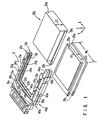
- Figures 1 and 2 a connector apparatus for memory cards in accordance with a preferred embodiment of the present invention.
- the term "memory card” refers to any plate-like integrated circuit card regardless of function, including those specified by the PCMCIA, JEIDA and JEDEC associations.
- the connector apparatus 12 of Figures 1 and 2 comprises upper and lower frames 12a and 12b which are coupled together in a stacked arrangement.
- Each frame 12a, 12b defines a respective storage deck 22a, 22b of the apparatus 12 and comprises a cross member 23a, 23b and a pair of side rails 13a, 13b that extend from the cross member and are spaced at an interval substantially equal to a width of a memory card.
- the cross member 23 and side rails 13 of each frame 12a, 12b form a generally U-shaped structure, one end of each frame 12a, 12b being open.
- Upper and lower headers 16a and 16b are coupled at the other end of each frame 12a, 12b proximate the respective cross members 23a, 23b.
- Each header 16a, 16b carries a respective array of contact pins 64a, 64b.
- additional frames can be stacked on top of frames 12a and 12b to form additional storage decks.
- the HDD package 20b has a thickness t 2 and comprises a base plate section 20c, and a housing 20d containing the actual hard disk drive (not shown).
- the housing 20d has a width smaller than that of the base plate section 20c.
- the base plate section 20c has substantially the same width and height as one of the memory cards 20a.
- the base plate section 20c When the HDD package 20b is inserted into the connector apparatus 12, the base plate section 20c is guided along the slots 24b in the side rails 13b of the lower frame 12b. Due to its thickness t 2 , the HDD package will occupy both the upper and lower storage decks 22a,b when fully inserted into the connector apparatus 12.
- An I/O socket is disposed in the forward end 20e of each memory card 20a and the HDD package 20b for connecting to the contact pins 64a,b of the respective headers 16a,b.
- Upper and lower ejecting mechanisms 40a and 40b are coupled to the upper and lower frames 12a, 12b, respectively.
- the upper and lower ejecting mechanisms 40a,b are identical.
- the upper ejecting mechanism 40a has a lever 42a pivotally supported on the cross member 23a of the upper frame 12a.
- One end of the lever 42a is coupled to a push rod 44a.
- the push rod 44a is inserted into a guide frame 46a mounted on an outer side surface of the upper frame 12a and is slidable along the Y direction.
- the other end of the lever 42a has a claw 46a which, through an opening 44a in the cross member 23a, engages with a slide plate 48a (Fig. 3) as described below.
- Fig. 3 is a bottom view showing the slide plate 48a.
- the slide plate 48a is disposed below the cross member 23a of the upper frame 12a and has a substantially U-shaped configuration with a pair of legs 50a.
- Each leg 50a has a claw 52a extending substantially perpendicular thereto.
- the claws 52a of the slide plate 48a are guided in corresponding grooves formed in the upper surface of the side rails 13a of the upper frame 12a proximate the cross member 23a.
- the slide plate 48a has a pair of hooks 56a near its forward end that engage with the forward end 20e of a memory card inserted into the upper storage deck 22a.
- the slide plate 48a has a claw 58a at its middle that engages with the claw 46a of the lever 42a.
- a memory card e.g. memory card 20a
- its forward end 20e engages with the hooks 56a of the slide plate 48a causing the slide plate 48a to slide toward the header 16a.
- the I/O socket in the forward end 20e of the memory card electrically connects to the contact pins 64a of the upper header 16a.
- the push rod 44a is pushed toward the header 16a causing the lever 42a to pivot about its midpoint such that the claw 46a of the lever 42a engages with the claw 58a of the slide plate 48a thereby urging the slide plate 48a toward the open end of the upper frame 12a.
- the hooks 56a of the slide plate 48a engage with the forward end 20e of the memory card thereby forcing the card backward out of the upper storage deck 22a.
- Similar component parts (not shown) of the lower ejecting mechanism 40b are arranged between the upper and lower frames 12a, 12b.
- the lower ejecting mechanism 40b operates to eject memory cards from the lower deck 22b.
- the lower ejecting mechanism 40b is used to eject the HDD package.
- the lower frame 12b of the dual storage deck apparatus 12 is mounted on a printed circuit board 60 which is omitted in Fig. 1 for convenience of illustration only. Respective interface circuits (not shown) for the upper and lower headers 16a and 16b may be printed on the printed circuit board 60.
- the upper header 16a of the connector apparatus 12 has a plurality of L-shaped contact pins 62a with upturned solder tails 64a.
- the solder tails 64a of upper array of contact pins 62a are inserted through corresponding solder holes in a small printed circuit board 66 and are soldered thereto.
- a receptacle 70 of a surface mount vertical connector 68 is mounted on the lower surface of the small printed circuit board 66.
- Terminals 72a of the receptacle 70 are soldered to the small printed circuit board 66.
- the small printed circuit board 66 connects each terminal 72a to a respective one of the solder tails 64a, in a one-to-one correspondence. Essentially, therefore, each terminal 72a is an extension of a respective one of the contact pins 62a of the upper header 16a.
- a mating header 74 of the face mount vertical connector 68 is mounted on the printed circuit board 60. Mating terminals 72b of the header 74 are soldered to the printed circuit board 60.
- the lower header 16b of the connector apparatus has a plurality of contact pins 62b. Down-turned solder tails 64b of the contact pins 62b of the lower header 16b are soldered directly to their corresponding connection points on the main printed circuit board 60.
- the small printed circuit board 66 and vertical connector 68 serve to connect each of the contact pins 62a of the upper header 16a to respective signal traces on the main printed circuit board 60.
- the contact pins 62b of the lower header 16b are directly connected to the circuit board 60
- the contact pins 62a of the upper header 16a are indirectly connected to the circuit board 60 via the small circuit board 66 and vertical connector 68.
- a space S is defined between the lower header 16b of the connector apparatus and the header 74 of the vertical connector 68.
- Various circuit components may be mounted to the printed circuit board in space S.
- the connector apparatus is assembled to the printed circuit board 60 as defined in claim 9.
- the lower header 16b is directly connected to the printed circuit board 60 and the upper header 16a is indirectly connected to the printed circuit board 60 via the small printed circuit board 66 and vertical connector 68.
- the upper and lower headers 16a and 16b are both connected to the circuit board 60 without the disadvantages that result from having to directly solder both headers to that circuit board 60.
Landscapes
- Engineering & Computer Science (AREA)
- Microelectronics & Electronic Packaging (AREA)
- Coupling Device And Connection With Printed Circuit (AREA)
- Multi-Conductor Connections (AREA)
Claims (11)
- Verbindungsvorrichtung (12) zum Verbinden einer Speicherkarte (20a, 20b) mit einer gedruckten Hauptleiterplatte (60), wobei die Verbindungsvorrichtung umfaßt:mindestens einen oberen und einen unteren Rahmen (12a, 12b), die in einer gestapelten Anordnung auf der Hauptleiterplatte (60) miteinander gekoppelt sind, wobei jeder Rahmen einander gegenüberliegende Seitenschienen (13a, 13b) aufweist, die in einem Intervall voneinander beabstandet sind, das im wesentlichen der Breite einer Speicherkarte (20a, 20b) entspricht, die Rahmen (12a, 12b) jeweilige Speicherdeckplätze (22a, 22b) definieren und Köpfe (16a, 16b) mit einer im oberen Speicherplatz angeordneten ersten Kontaktstiftanordnung (62a) und einer im unteren Speicherplatz angeordneten zweiten Kontaktstiftanordnung (62b) aufweisen, eine der Kontaktstiftanordnungen (62b) elektrisch direkt mit der gedruckten Hauptleiterplatte verbunden ist, auf der die gestapelten oberen und unteren Rahmen montiert sind, mehrteilige vertikale Verbindungseinrichtungen (68, 66) zum von der einen Kontaktstiftanordnung unabhängigen, indirekten Verbinden der anderen Kontaktstiftanordnung (62a) mit der gedruckten Hauptleiterplatte (60) vorgesehen sind, die mehrteilige vertikale Verbindungseinrichtung eine zweite gedruckte Leiterplatte (66) umfaßt, mit der die andere Kontaktstiftanordnung (62a) direkt elektrisch verbunden ist, und ein zwischen der Hauptleiterplatte und der zweiten Leiterplatte angeordnetes Verbindungselement (68) so beschaffen ist, daß es die Hauptleiterplatte elektrisch mit der zweiten Leiterplatte verbindet.
- Verbindungsvorrichtung nach Anspruch 1, bei der die eine Kontaktstiftanordnung (62b) und/oder die andere Kontaktstiftanordnung (62a) jeweils durch einen Lötprozeß elektrisch mit der Hauptleiterplatte (60) und/oder der zweiten Leiterplatte (66) verbunden ist.
- Verbindungsvorrichtung nach Anspruch 2, bei der der Lötprozeß eine Oberflächenmontagetechnik umfaßt.
- Verbindungsvorrichtung nach einem der Ansprüche 1 bis 3, bei der das Verbindungselement (68) der mehrteiligen Verbindungseinrichtung an die gedruckte Hauptleiterplatte (60) gelötet ist.
- Verbindungsvorrichtung nach einem der Ansprüche 1 bis 4, bei der das Verbindungselement der mehrteiligen Verbindungseinrichtung ein oberflächenmontiertes Verbindungselement (68) ist.
- Verbindungsvorrichtung nach Anspruch 1, bei der das Verbindungselement (68) der mehrteiligen Verbindungseinrichtung aus einem Kopfabschnitt (74) und einem passenden Fassungsabschnitt (70) zusammengesetzt ist, wobei entweder der Kopf- oder der Fassungsabschnitt an die gedruckte Hauptleiterplatte (60) und der andere der Abschnitt an die zweite gedruckte Leiterplatte (66) gelötet ist.
- Verbindungsvorrichtung nach einem der Ansprüche 1 bis 6, bei der die Kontaktstiftanordnungen (62a, 62b) voneinander beabstandet sind.
- Verbindungsvorrichtung nach einem der Ansprüche 1 bis 7, bei der die Kontaktstiftanordnungen (62a, 62b) in voneinander beabstandeten Positionen an der zweiten Leiterplatte (66) mit der Hauptleiterplatte (60) verbunden sind.
- Verfahren zum Zusammenbau einer Verbindungsvorrichtung (12) nach Anspruch 1 mit einer gedruckten Hauptleiterplatte (60), wobei das Verfahren die Schritte umfaßt:a) Befestigen des unteren Rahmens (12b) an der gedruckten Hauptleiterplatte (60);b) Löten (i) der Kontaktstiftanordnung (62b) des Kopfs (16b) des unteren Rahmens (12b) und (ii) von Anschlüssen (72b) eines Kopfes (74) des Verbindungselements (68) an die gedruckte Hauptleiterplatte (60);c) Zusammenbauen des oberen Rahmens (12a) der Verbindungsvorrichtung und des unteren Rahmens (12b);d) Einpassen einer Fassung (70) des Verbindungselements (68) über den Kopf (74) des Verbindungselements, wobei die Fassung (70) Anschlüsse (72a) aufweist, die elektrisch mit der zweiten gedruckten Leiterplatte (66) verbunden werden; unde) Löten der Kontaktstiftanordnung (62a) des Kopfs (16a) des oberen Rahmens (12a) an die zweite gedruckte Leiterplatte (66), wodurch die Kontaktstifte der Kontaktstiftanordnung (62a) des Kopfs (16a) des oberen Rahmens (12a) über die zweite Leiterplatte (66) und das Verbindungselement (68) elektrisch indirekt mit der gedruckten Hauptleiterplatte (60) verbunden werden.
- Verfahren nach Anspruch 9, bei dem zumindest einer der Lötschritte (b) und (e) gemäß einer Oberflächenmontage-Löttechnik ausgeführt wird.
- Verfahren nach Anspruch 10, das ferner vor der Ausführung des Schritts (b) den Schritt der Beschichtung vorgegebener Bereiche der gedruckten Hauptleiterplatte (60) mit einer Lötpaste umfaßt.
Applications Claiming Priority (4)
| Application Number | Priority Date | Filing Date | Title |
|---|---|---|---|
| JP13477/93U | 1993-03-23 | ||
| JP1347793U | 1993-03-23 | ||
| JP1993013477U JP2567629Y2 (ja) | 1993-03-23 | 1993-03-23 | コネクタ装置 |
| PCT/US1994/003135 WO1994022182A1 (en) | 1993-03-23 | 1994-03-23 | Connector apparatus |
Publications (3)
| Publication Number | Publication Date |
|---|---|
| EP0696387A1 EP0696387A1 (de) | 1996-02-14 |
| EP0696387A4 EP0696387A4 (de) | 1998-04-01 |
| EP0696387B1 true EP0696387B1 (de) | 2003-01-02 |
Family
ID=11834210
Family Applications (1)
| Application Number | Title | Priority Date | Filing Date |
|---|---|---|---|
| EP94912291A Expired - Lifetime EP0696387B1 (de) | 1993-03-23 | 1994-03-23 | Verbindungsvorrichtung |
Country Status (6)
| Country | Link |
|---|---|
| US (1) | US6287143B1 (de) |
| EP (1) | EP0696387B1 (de) |
| JP (1) | JP2567629Y2 (de) |
| DE (1) | DE69431951T2 (de) |
| SG (1) | SG47758A1 (de) |
| WO (1) | WO1994022182A1 (de) |
Families Citing this family (20)
| Publication number | Priority date | Publication date | Assignee | Title |
|---|---|---|---|---|
| DE4438389A1 (de) * | 1994-10-27 | 1996-05-02 | Zeiss Carl Fa | Verfahren und Anordnung zur Anregung eines Gaslasers über eine Hochspannungsentladung |
| EP0801823B1 (de) * | 1995-01-06 | 2003-05-02 | Fci | Abgeschirmter speicherkartensteckverbinder |
| JP3066570B2 (ja) * | 1996-07-26 | 2000-07-17 | モレックス インコーポレーテッド | Pcカード用コネクタアッセンブリの製造方法 |
| JPH10255881A (ja) * | 1997-03-07 | 1998-09-25 | Molex Inc | 信号端子とグランド端子を備えた電気コネクタ |
| US6604955B2 (en) * | 2001-11-02 | 2003-08-12 | Avaya Technology Corp. | Electronic circuit protection device |
| CN2626090Y (zh) * | 2003-05-21 | 2004-07-14 | 莫列斯公司 | 双端口式电子卡连接器接头 |
| US6955224B2 (en) * | 2003-09-10 | 2005-10-18 | Watson Philip K | Casing alignment tool |
| TWM261893U (en) * | 2004-08-27 | 2005-04-11 | Molex Taiwan Ltd | Electrical connector |
| WO2006097780A1 (en) * | 2005-03-17 | 2006-09-21 | Nokia Corporation | Universal card holder for electronic devices |
| US7987584B2 (en) * | 2008-02-04 | 2011-08-02 | International Business Machines Corporation | Article extraction / insertion tool and assembly |
| US8172586B2 (en) * | 2009-10-14 | 2012-05-08 | Horng Yu Tsai | Multilayer electronic card connector with ejector |
| JP5614979B2 (ja) * | 2009-12-22 | 2014-10-29 | キヤノン株式会社 | 電子機器 |
| TWI372967B (en) * | 2010-03-15 | 2012-09-21 | Wistron Corp | Unloading mechanism for unloading an electronic component and computer device thereof |
| TW201232928A (en) * | 2011-01-17 | 2012-08-01 | Walton Advanced Eng Inc | Data storage device |
| CN102324654B (zh) * | 2011-08-24 | 2013-10-09 | 鸿富锦精密工业(深圳)有限公司 | 具有顶出机构的电子设备 |
| US9557783B2 (en) * | 2015-01-27 | 2017-01-31 | Hewlett Packard Enterprise Development Lp | Configurable card slots |
| CN110255314B (zh) * | 2019-06-24 | 2021-03-30 | 上海贝思特电气有限公司 | 一种电梯显示器 |
| EP3923687B1 (de) | 2020-06-09 | 2024-04-03 | Samsung Electronics Co., Ltd. | Speichervorrichtung und elektronische vorrichtung damit |
| CN112003098B (zh) * | 2020-08-25 | 2021-11-09 | 立讯精密工业股份有限公司 | 转接装置 |
| USD997161S1 (en) | 2020-09-10 | 2023-08-29 | Samsung Electronics Co., Ltd. | Solid state drive memory device |
Family Cites Families (49)
| Publication number | Priority date | Publication date | Assignee | Title |
|---|---|---|---|---|
| US3466591A (en) | 1964-10-30 | 1969-09-09 | Olivetti & Co Spa | Electrical connector for printed-circuit boards |
| FR1604177A (de) | 1968-12-27 | 1971-07-26 | ||
| FR2114169A6 (de) | 1970-11-18 | 1972-06-30 | Honeywell Bull | |
| US3676746A (en) | 1970-12-23 | 1972-07-11 | Honeywell Inf Systems | Compatible modular circuit board connector |
| US3767974A (en) * | 1972-01-03 | 1973-10-23 | Cogar Corp | Insertion and extraction lever for printed circuit cards |
| US4445740A (en) * | 1982-04-26 | 1984-05-01 | Rockwell International Corporation | Circuit board assembly |
| US4600256A (en) | 1984-12-31 | 1986-07-15 | Motorola, Inc. | Condensed profile electrical connector |
| US4858070A (en) | 1987-04-24 | 1989-08-15 | Racal Data Communications Inc. | Modular expandable housing arrangement for electronic apparatus |
| US4755911A (en) | 1987-04-28 | 1988-07-05 | Junkosha Co., Ltd. | Multilayer printed circuit board |
| US4789352A (en) * | 1987-12-02 | 1988-12-06 | Amp Incorporated | Power connector having linearly moving cam for daughter card |
| JPH0633656Y2 (ja) | 1987-12-21 | 1994-08-31 | 株式会社村田製作所 | 表面実装型コネクタ |
| JPH0541509Y2 (de) * | 1988-03-03 | 1993-10-20 | ||
| KR920008949B1 (ko) * | 1988-04-30 | 1992-10-12 | 후지쓰 가부시끼가이샤 | 전자회로장치의 프린트기판 유니트(printed board unit)착탈기구 |
| US4929185A (en) * | 1989-04-03 | 1990-05-29 | Nrc Corporation | Printed circuit board assembly |
| US4996631A (en) * | 1989-10-30 | 1991-02-26 | Canoga Industries, Inc. | Injector/ejector system for rack mounted plug-in modules with front panels |
| US5113317A (en) | 1990-02-20 | 1992-05-12 | Allen-Bradley Company, Inc. | Support for auxiliary circuit card |
| US5151033A (en) | 1990-09-13 | 1992-09-29 | Hirose Electric Co., Ltd. | Electrical connector |
| US5085590A (en) | 1990-10-30 | 1992-02-04 | Amp Incorporated | Shielded stackable connector assembly |
| US5224019A (en) | 1991-03-15 | 1993-06-29 | Amkly Systems, Inc. | Modular computer assembly |
| US5176523A (en) * | 1991-08-09 | 1993-01-05 | Foxconn International, Inc. | Stackable memory card connector |
| US5201662A (en) | 1991-08-23 | 1993-04-13 | Molex Incorporated | Electrical connector for mounting on a printed circuit board |
| JP2659030B2 (ja) | 1991-09-12 | 1997-09-30 | デュポン・シンガポール・ピーティーイー・リミテッド | コネクタ装置 |
| US5283713A (en) * | 1991-09-20 | 1994-02-01 | Nec Corporation | Injector/ejector system for a plug-in module and apparatus using the systems |
| US5299089A (en) | 1991-10-28 | 1994-03-29 | E. I. Dupont De Nemours & Co. | Connector device having two storage decks and three contact arrays for one hard disk drive package or two memory cards |
| US5149276A (en) * | 1991-12-18 | 1992-09-22 | Amp Incorporated | Modular holder having an ejector mechanism for a dual IC package |
| US5194010A (en) | 1992-01-22 | 1993-03-16 | Molex Incorporated | Surface mount electrical connector assembly |
| US5224865A (en) | 1992-02-24 | 1993-07-06 | Hughes Aircraft Company | Sliding wedge electrical connector |
| US5225968A (en) | 1992-03-10 | 1993-07-06 | Ma Hsi K | Connecting apparatus for connecting computer functional cards to a mother board |
| US5161999A (en) | 1992-03-18 | 1992-11-10 | Amp Incorporated | Surface mount electrical cohnnector and shield therefor |
| DE9204884U1 (de) * | 1992-04-08 | 1992-07-30 | Ma, Hsi Kuang, Taipeh/T'ai-pei | Kombinationssteckverbinder für Computer-Interfacekarten |
| US5260854A (en) | 1992-05-14 | 1993-11-09 | Sun Microsystems, Inc. | Modular circuit board placement system |
| US5259783A (en) | 1992-05-15 | 1993-11-09 | Sun Microsystems, Inc. | Dual height card retainer |
| US5290174A (en) * | 1992-08-10 | 1994-03-01 | The Whitaker Corporation | Electrical connector for a card reader |
| US5297966A (en) | 1992-08-10 | 1994-03-29 | The Whitaker Corporation | Mounting bracket for an electrical connector |
| US5318452A (en) * | 1992-08-10 | 1994-06-07 | The Whitaker Corporation | Electrical connector |
| US5308251A (en) | 1992-08-10 | 1994-05-03 | The Whitaker Corporation | Mounting bracket with ESD protection for an electrical connector |
| US5268820A (en) | 1992-08-18 | 1993-12-07 | Mitac International Corp. | Mother board assembly |
| US5217394A (en) | 1992-09-10 | 1993-06-08 | Ho Ming Chiao | Converter-type circuit connector for linking electronic devices |
| US5277615A (en) | 1992-09-24 | 1994-01-11 | Compaq Computer Corporation | Apparatus for removably supporting a plurality of hot plug-connected hard disk drives |
| US5305182A (en) | 1992-10-14 | 1994-04-19 | Chen Teng Ka | Read/write unit for two integrated circuit cards |
| US5415569A (en) | 1992-10-19 | 1995-05-16 | Molex Incorporated | Filtered electrical connector assembly |
| US5408386A (en) | 1992-10-30 | 1995-04-18 | Intel Corporation | Socket assembly including a first circuit board located between a receptacle housing and a second circuit board |
| US5286207A (en) | 1992-12-21 | 1994-02-15 | Foxconn International, Inc. | Memory card connector |
| JP2603509Y2 (ja) | 1992-12-28 | 2000-03-15 | 日本エー・エム・ピー株式会社 | カードエッジコネクタ |
| US5334046A (en) | 1993-02-22 | 1994-08-02 | Augat Inc. | Circuit card interface system |
| US5316488A (en) | 1993-06-04 | 1994-05-31 | Molex Incorporated | Connector apparatus for IC packs |
| US5267876A (en) | 1993-06-16 | 1993-12-07 | The Whitaker Corporation | Board saving stacked electrical connector assembly |
| US5399105A (en) | 1994-04-29 | 1995-03-21 | The Whitaker Corporation | Conductive shroud for electrical connectors |
| US5478260A (en) | 1994-07-29 | 1995-12-26 | The Whitaker Corporation | Grounding for electrical connectors |
-
1993
- 1993-03-23 JP JP1993013477U patent/JP2567629Y2/ja not_active Expired - Lifetime
-
1994
- 1994-03-23 WO PCT/US1994/003135 patent/WO1994022182A1/en not_active Ceased
- 1994-03-23 SG SG1996004243A patent/SG47758A1/en unknown
- 1994-03-23 DE DE69431951T patent/DE69431951T2/de not_active Expired - Lifetime
- 1994-03-23 EP EP94912291A patent/EP0696387B1/de not_active Expired - Lifetime
-
1999
- 1999-03-17 US US09/270,706 patent/US6287143B1/en not_active Expired - Fee Related
Also Published As
| Publication number | Publication date |
|---|---|
| JP2567629Y2 (ja) | 1998-04-02 |
| DE69431951D1 (de) | 2003-02-06 |
| EP0696387A1 (de) | 1996-02-14 |
| US6287143B1 (en) | 2001-09-11 |
| WO1994022182A1 (en) | 1994-09-29 |
| JPH0672167U (ja) | 1994-10-07 |
| SG47758A1 (en) | 1998-04-17 |
| DE69431951T2 (de) | 2003-09-04 |
| EP0696387A4 (de) | 1998-04-01 |
Similar Documents
| Publication | Publication Date | Title |
|---|---|---|
| US6287143B1 (en) | Multi-storage deck connector apparatus | |
| US5451168A (en) | Connector apparatus for memory cards having a one-piece integrated frame | |
| US5470259A (en) | Grounding shroud for surface mounted electrical connector | |
| US6488542B2 (en) | Type III PCMCIA card with integrated receptacles for receiving standard communications plugs | |
| US5984731A (en) | Removable I/O device with integrated receptacles for receiving standard plugs | |
| US6048214A (en) | Card connector with improved grounding terminal | |
| US6174197B1 (en) | Card connector assembly | |
| US5967803A (en) | Card connector | |
| US5906510A (en) | Multi-storage deck connector apparatus | |
| KR20030082975A (ko) | 대용량 메모리 카드용 전기 커넥터 | |
| US7063539B2 (en) | Memory card connector with auxiliary printed circuit board | |
| US6554627B1 (en) | Electronic card connector and method for assembling same | |
| US5427534A (en) | Connector with side-swipe contacts | |
| US6454574B1 (en) | Electrical card connector | |
| KR100325971B1 (ko) | 향상된접지단자를갖는카드커넥터 | |
| US20060160424A1 (en) | Electrical connector assembly having board hold down | |
| US6116920A (en) | Alignment socket for PCMCIA card connector | |
| US20050215084A1 (en) | Board mounted memory card connector | |
| EP0654870A2 (de) | Haltevorrichtung für IC-Karteverbinder | |
| KR20010002369U (ko) | 카드 커넥터 조립체 | |
| US20050079764A1 (en) | Memory card connector for mounting on a printed circuit board | |
| JPH11307202A (ja) | イジェクト機構付きカード用コネクタ装置 | |
| JPH11297433A (ja) | イジェクト機構付きカード用コネクタ装置 |
Legal Events
| Date | Code | Title | Description |
|---|---|---|---|
| PUAI | Public reference made under article 153(3) epc to a published international application that has entered the european phase |
Free format text: ORIGINAL CODE: 0009012 |
|
| 17P | Request for examination filed |
Effective date: 19951019 |
|
| AK | Designated contracting states |
Kind code of ref document: A1 Designated state(s): DE FR GB |
|
| RAP1 | Party data changed (applicant data changed or rights of an application transferred) |
Owner name: CONNECTOR SYSTEMS TECHNOLOGY N.V. Owner name: BERG ELECTRONICS MANUFACTURING B.V. |
|
| A4 | Supplementary search report drawn up and despatched |
Effective date: 19980209 |
|
| AK | Designated contracting states |
Kind code of ref document: A4 Designated state(s): DE FR GB |
|
| 17Q | First examination report despatched |
Effective date: 19980512 |
|
| RAP1 | Party data changed (applicant data changed or rights of an application transferred) |
Owner name: BERG ELECTRONICS MANUFACTURING B.V. |
|
| GRAG | Despatch of communication of intention to grant |
Free format text: ORIGINAL CODE: EPIDOS AGRA |
|
| GRAG | Despatch of communication of intention to grant |
Free format text: ORIGINAL CODE: EPIDOS AGRA |
|
| GRAH | Despatch of communication of intention to grant a patent |
Free format text: ORIGINAL CODE: EPIDOS IGRA |
|
| GRAH | Despatch of communication of intention to grant a patent |
Free format text: ORIGINAL CODE: EPIDOS IGRA |
|
| GRAA | (expected) grant |
Free format text: ORIGINAL CODE: 0009210 |
|
| AK | Designated contracting states |
Kind code of ref document: B1 Designated state(s): DE FR GB |
|
| RIC1 | Information provided on ipc code assigned before grant |
Free format text: 7H 01R 12/04 A, 7H 01R 12/32 B, 7H 01R 12/18 B, 7H 01R 12/20 B, 7H 05K 5/02 B |
|
| REG | Reference to a national code |
Ref country code: GB Ref legal event code: FG4D Free format text: 20030102 |
|
| REF | Corresponds to: |
Ref document number: 69431951 Country of ref document: DE Date of ref document: 20030206 Kind code of ref document: P |
|
| PGFP | Annual fee paid to national office [announced via postgrant information from national office to epo] |
Ref country code: FR Payment date: 20030326 Year of fee payment: 10 |
|
| PG25 | Lapsed in a contracting state [announced via postgrant information from national office to epo] |
Ref country code: GB Free format text: LAPSE BECAUSE OF NON-PAYMENT OF DUE FEES Effective date: 20030402 |
|
| ET | Fr: translation filed | ||
| PLBE | No opposition filed within time limit |
Free format text: ORIGINAL CODE: 0009261 |
|
| STAA | Information on the status of an ep patent application or granted ep patent |
Free format text: STATUS: NO OPPOSITION FILED WITHIN TIME LIMIT |
|
| GBPC | Gb: european patent ceased through non-payment of renewal fee |
Effective date: 20030402 |
|
| 26N | No opposition filed |
Effective date: 20031003 |
|
| PG25 | Lapsed in a contracting state [announced via postgrant information from national office to epo] |
Ref country code: FR Free format text: LAPSE BECAUSE OF NON-PAYMENT OF DUE FEES Effective date: 20041130 |
|
| REG | Reference to a national code |
Ref country code: FR Ref legal event code: ST |
|
| PGFP | Annual fee paid to national office [announced via postgrant information from national office to epo] |
Ref country code: DE Payment date: 20120330 Year of fee payment: 19 |
|
| REG | Reference to a national code |
Ref country code: DE Ref legal event code: R119 Ref document number: 69431951 Country of ref document: DE Effective date: 20131001 |
|
| PG25 | Lapsed in a contracting state [announced via postgrant information from national office to epo] |
Ref country code: DE Free format text: LAPSE BECAUSE OF NON-PAYMENT OF DUE FEES Effective date: 20131001 |