EP0696846B1 - Hochpassfilterstruktur mit programmierbaren Nullstellen - Google Patents
Hochpassfilterstruktur mit programmierbaren Nullstellen Download PDFInfo
- Publication number
- EP0696846B1 EP0696846B1 EP94830401A EP94830401A EP0696846B1 EP 0696846 B1 EP0696846 B1 EP 0696846B1 EP 94830401 A EP94830401 A EP 94830401A EP 94830401 A EP94830401 A EP 94830401A EP 0696846 B1 EP0696846 B1 EP 0696846B1
- Authority
- EP
- European Patent Office
- Prior art keywords
- filter
- accordance
- input
- node
- output
- Prior art date
- Legal status (The legal status is an assumption and is not a legal conclusion. Google has not performed a legal analysis and makes no representation as to the accuracy of the status listed.)
- Expired - Lifetime
Links
- 239000003990 capacitor Substances 0.000 claims description 12
- 102000016550 Complement Factor H Human genes 0.000 description 3
- 108010053085 Complement Factor H Proteins 0.000 description 3
- 238000005516 engineering process Methods 0.000 description 2
- 230000005540 biological transmission Effects 0.000 description 1
- 230000001934 delay Effects 0.000 description 1
- 230000000694 effects Effects 0.000 description 1
- 238000001914 filtration Methods 0.000 description 1
- 230000010354 integration Effects 0.000 description 1
- 230000004048 modification Effects 0.000 description 1
- 238000012986 modification Methods 0.000 description 1
- 238000011144 upstream manufacturing Methods 0.000 description 1
Images



Classifications
-
- H—ELECTRICITY
- H03—ELECTRONIC CIRCUITRY
- H03H—IMPEDANCE NETWORKS, e.g. RESONANT CIRCUITS; RESONATORS
- H03H11/00—Networks using active elements
- H03H11/02—Multiple-port networks
- H03H11/04—Frequency selective two-port networks
- H03H11/0422—Frequency selective two-port networks using transconductance amplifiers, e.g. gmC filters
- H03H11/0433—Two integrator loop filters
Definitions
- the present invention relates to a programmable-zeros filter specifically for high-frequency applications.
- the present invention relates to a high-pass filter in particular for high-frequency applications and of the type comprising at least one input terminal and at least one output terminal between which is defined a transfer function and is inserted a biquadratic cell incorporating a series of transconductance stages.
- the cell 1 of FIG. 1 has a conventional structure as shown for simplicity of description in a single-ended configuration.
- the cell 1 it is however possible to provide configuration of the fully-differential type which improves rejection of common mode signals and disturbances from the power lines.
- the cell 1 has an input terminal IN and an output terminal OUT between which is inserted the cascade of a first 2, a second 3 and a third 4 transconductance stages.
- a fourth stage 5 is connected with a feedback 19 between an output of the third stage 4 and an input of the second stage 3.
- the first stage 2 has an input 6 connected directly with the input terminal IN of the cell 1 and is designed to receive a voltage signal Vin.
- This first stage 2 has its output 7 connected to an input terminal 8 of the second stage 3 forming a first circuit node A.
- the circuit node A is connected to a voltage reference, e.g. a signal ground GND, by means of a first capacitor C1.
- the second stage 3 has in turn an output 9 connected to an input 10 of the third stage 4 forming a second circuit node B.
- circuit node B is connected to ground by means of a second capacitor C2.
- the third stage 4 has an output 11 connected to an input 12 of the fourth transconductance stage 5 by means of a feedback connection 19 and the output 11 coincides virtually with the second node B.
- This circuit node B coincides also with the output terminal OUT of the cell 1 from which is taken an output voltage Vout.
- the fourth transconductance stage 5 has an output terminal 13 connected in feedback to the first circuit node A.
- the high-pass or all-pass functions are obtained generally starting from a biquadratic cell 1 of the low-pass type such as that discussed with reference to FIG. 1.
- a first known solution as shown in FIG. 2 is virtually taken from the cell 1 replacing the capacitors C1 and C2 with respective variable capacitors CV1 and CV2.
- Said variable capacitors CV1, CV2 are connected between the circuit nodes A and B respectively and the input terminal 6 of the first stage 2.
- the biquadratic cell thus obtained which we shall indicated by reference number 14, is the high-pass type but is not immune to its own shortcomings because of the variable and floating capacitances imposed by a high capacitive load at input.
- transfer function FdT of this cell 14 exhibits at the numerator some "zeros" which are difficult to vary or modify.
- the known art proposes also a second solution, again taken from the biquadratic cell 1 of low-pass type.
- This second solution is indicated by 15 in FIG. 3 and proposes the introduction of operational amplifiers 16 and 17 with variable gain K1 and K2 and inserted between the capacitors C1 and C2 and the input terminal 6. In this manner there is obtained a biquadratic cell 15 of high-pass type which permits obtaining the variability of the zeros present at the numerator of the transfer function.
- the cell 15 introduces strong signal distortions if the transmission delays for the paths indicated in the figures by PATH1, PATH2 and PATH3 are unequal. Since the first PATH1 of said paths is very fast and high-frequency, even the second PATH2 and the third path PATH3 should be equally fast.
- PATH2 and PATH3 would require a strong bias current of the operational amplifiers 16 and 17 and this would have for its immediate consequence a high power dispersal.
- the technical problem underlying the present invention is to conceive a high-pass filter structure having structural and functional characteristics capable of overcoming the shortcomings which still afflict the devices provided in accordance with the known art.
- the technical problem is to conceive a biquadratic cell operating on low voltage power supply and not requiring the presence of floating capacitance and having low capacitive load at input.
- the solution idea underlying the present invention is to make available a filter structure having a transfer function presenting a current gain instead of a voltage gain.
- reference number 20 indicates as a whole a high-pass filter structure provided in accordance with the present invention for high frequency applications.
- the filter 20 is first illustrated in a so-called single-ended configuration.
- the filter 20 comprises a high-pass biquadratic cell 18 which has a structure similar to the low-pass cell 1 discussed above. In particular, even the high-pass biquadratic cell 18 exhibits circuitry nodes A and B upstream and downstream respectively of the second stage 3.
- the nodes A and B are connected to a current generator circuit 29 generating currents i K1 and i K2 .
- Vout/Vin [gm1*gm2/(C1*C2) + s*(C K1 *gm2)/(C1*C2)*A1 - s2*C K2 /C2*A2)/(s2 + s*(gm3/C2) + gm2*gm4/(C1*C2)
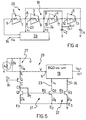
- FIG. 5 shows in detail an embodiment of the current generator circuit 29 for the biquadratic cell 18 of the low-pass filter 20.
- the circuit nodes A and B are connected to ground by means of a current mirror structure comprising a pair of bipolar npn transistors Q2 and Q3 respectively with respective base terminals B2 and B3 connected together and to the base terminal B1 of another bipolar npn transistor Q1.
- the emitter terminals E1, E2 and E3 of the bipolar transistors Q1, Q2 and Q3 are all connected together and to the signal ground reference GND. Said terminals are traversed by bias currents I1, I2 and I3.
- a first current mirror 21 comprises the transistors Q1 and Q2 while a second current mirror 22 comprises the transistors Q1 and Q3.
- the third bipolar npn transistor Q1 has base B1 and collector C1 short-circuited.
- a first branch 23 of the mirror 21 is connected to the node A while a second branch 24 of the current mirror 22 is connected to the node B.
- the branches 23 and 24 lead to the collectors of threshold transistors Q2 and Q3.
- a fourth bipolar pnp transistor Q is inserted in the current generator circuit 29 in connection with the third bipolar npn transistor Q1 and with the input 6 of the first stage 2.
- Said bipolar pnp transistor Q has the collector terminal C connected to the collector C1 of the bipolar npn transistor Q1 and the emitter terminal E connected to the input 6.
- the emitter terminal E is connected to ground GND by means of an impedance 27 comprising the parallel of a capacitor C K and of a current generator I1 having an output conductance g O .
- This impedance 27 consists essentially of a conductance parallel.
- the bipolar pnp transistor Q receives on its base terminal B the input voltage Vin.
- the current generator circuit 29 supplies to the input 6 of the high-pass biquadratic cell 18 a voltage V given by the product of Vin * H(s) where H(s) is a programmable factor determining the principal pole of the input structure.
- H(s) 1/[1 + (g CE + g O )/gm] * [1/(1 + s*C K /gm + g CE +g O )] where:
- the gain of the circuit 29 is a current gain instead than a voltage gain.
- the double current mirror 21, 22 introduces in the transfer function of the low-pass filter 20 another pole having however a negligible effect on the total phase.
- the presence of the programmable factor H(s) does not introduce distortions in the output signal of the high-pass biquadratic cell 18 because it is present in all the signals.
- the high-pass filter 20 in accordance with the present invention does not exhibit floating capacitance, overcoming one of the problems afflicting the known art.
- the filter 20 exhibits double input terminals IN- AND IN+ which are inverting and non-inverting respectively and double output terminals OUT- and OUT+.
- the biquadratic cell 28 incorporated in the filter 20 provides a cascade of differential stages 32, 33, 34 and 35 with transconductance.
- the generator circuit 29a provided again with bipolar technology is illustrated in FIGS. 7 and 8.
- the first mirror 41 comprises the transistors Q1 and Q2 while the second mirror 42 comprises the transistors Q1 and Q3. Since the structure is the differential type the transistors were doubled in relation to the example of FIG. 5 and there are provided virtually double current mirrors 41 and 42 having respective branches 23a, 23b and 24a, 24b connected to the corresponding differential outputs of the stages 32 and 33.
- the emitters of the transistors Q2 are connected to ground by means of a variable bias current generator 2I2.
- the mirror relationships are modified and hence the coefficients of the transfer function FdT of the filter change.
- the coefficients which are modified are just those present at the numerator of the transfer function FdT and hence the "zeroes".
- a compensation block 25 is inserted between the differential inputs IN- and IN+ of the biquadratic cell 28.
- FIGS. 9a, 9b and 9c show possible alternative embodiments of said compensation block 25 incorporating a pair of capacitors C K in series or parallel.
- the pair of capacitors C K is connected between the differential inputs IN+,IN- and a signal ground.
- FIG. 8 shows an embodiment of the current generator circuit 29 comprising only bipolar npn transistors.
- the different arrangement of the compensation block 25 and transistors Q and Q1 is quite clear to those skilled in the art.
- an embodiment of the current generator circuit 29 with CMOS technology is easy to define by means of a regular replacement of the bipolar npn transistors with N-channel MOS transistors and an analogous replacement of the bipolar pnp transistors with P-channel MOS transistors.
Landscapes
- Networks Using Active Elements (AREA)
Claims (10)
- Hochpassfilter, insbesondere für Hochfrequenzanwendungen, wobei das Hochpassfilter mindestens einen Eingangsanschluss (IN) und mindestens einen Ausgangsanschluss (OUT) umfasst, zwischen denen eine Transferfunktion (FdT) definiert ist und eine biquadratische Zelle (18) eingefügt ist, die eine Reihe von Transkonduktanz-Stufen (2, 3, 4, 5)enthält, und dadurch gekennzeichnet ist, dass das Filter weiter einen Generatorkreis (29) umfasst, der an den Eingangsanschluss (IN), an einen ersten Knoten (A), der an einer direkten Verbindung zwischen dem Ausgang einer ersten (2) der Transkonduktanz-Stufen und dem Eingang einer zweiten (3) der Transkonduktanz-Stufen vorgesehen ist, und an einen zweiten Knoten (B), der an einer direkten Verbindung zwischen dem Ausgang der zweiten (3) der Transkonduktanz-Stufen und dem Eingang einer dritten (4) der Transkonduktanz-Stufen der biquadratischen Zelle (18) vorgesehen ist, sowie an eine Spannungsreferenz (GND) angeschlossen ist, wobei der Generatorkreis (29) mindestens einen ersten (iK1) und einen zweiten variablen Strom (iK2) erzeugt, die dynamisch in Übereinstimmung mit Signalen, die an dem Eingangsanschluss (IN) empfangen werden, variiert werden, um die Nullen in der Transferfunktion (FdT) des Filters (20) programmierbar zu machen, wobei der erste variable Strom (iK1) an den ersten Knoten (A) geliefert wird und der zweite variable Strom (iK2) an den zweiten Knoten (B) geliefert wird.
- Filter nach Anspruch 1, dadurch gekennzeichnet, dass der Stromgeneratorkreis (29) einen Stromspiegelaufbau mit mindestens einem ersten Abzweig (23), der an den ersten Knoten angeschlossen ist, und mindestens einem zweiten Abzweig (24), der an den zweiten Knoten angeschlossen ist, umfasst.
- Filter nach Anspruch 2, dadurch gekennzeichnet, dass der erste Abzweig (23) direkt zwischen dem Ausgang der ersten Stufe (2) und der Spannungsreferenz (GND) angeschlossen ist und der zweite Abzweig (24) zwischen dem Ausgang der zweiten Stufe (3) und der Spannungsreferenz (GND) angeschlossen ist.
- Filter nach Anspruch 1, dadurch gekennzeichnet, dass es auch eine Impedanz (27), die zwischen dem Eingangsanschluss (IN) und dem ersten (2) der Stufen eingefügt ist, umfasst.
- Filter nach Anspruch 4, dadurch gekennzeichnet, dass die Impedanz (27) die Parallele eines Kondensators (CK) und eines Stromgenerators (I1) mit vorbestimmter Ausgangskonduktanz (g0) umfasst.
- Filter nach Anspruch 2, dadurch gekennzeichnet, dass der Stromspiegelaufbau ein Paar bipolarer Transistoren (Q2, Q3) mit entsprechenden Basisanschlüssen (B2,B3), die zusammengeschlossen und an den Basisanschluss (B1) eines dritten bipolaren Transistors (Q1) angeschlossen sind, umfasst, wobei die Transistoren ihre entsprechenden Emitter gemeinsam haben und an die Spannungsreferenz (GND) angeschlossen sind.
- Filter nach Anspruch 6, dadurch gekennzeichnet, dass es einen vierten bipolaren Transistor (Q), der in den Generatorkreis (29) in Verbindung mit dem dritten Transistor (Q1) und mit dem Eingang (6) der ersten (2) der Stufen eingefügt ist, unfasst.
- Filter nach Anspruch 7, dadurch gekennzeichnet, dass der vierte Transistor (Q) vom pnp-Typ ist und mit seinem Kollektoranschluss (C) an den Kollektor (C1) des dritten Transistors (Q1) und mit dem Emitteranschluss (E) an den Eingang (6) angeschlossen ist.
- Filter nach Anspruch 3, dadurch gekennzeichnet, dass die Spiegelbeziehung zwischen dem ersten Stromspiegel (21) und dem zweiten Stromspiegel (22) programmierbar ist.
- Filter nach Anspruch 1, dadurch gekennzeichnet, dass die Verstärkung der biquadratischen Zelle (18) im Strom liegt.
Priority Applications (4)
| Application Number | Priority Date | Filing Date | Title |
|---|---|---|---|
| EP94830401A EP0696846B1 (de) | 1994-08-12 | 1994-08-12 | Hochpassfilterstruktur mit programmierbaren Nullstellen |
| DE69431656T DE69431656D1 (de) | 1994-08-12 | 1994-08-12 | Hochpassfilterstruktur mit programmierbaren Nullstellen |
| US08/455,850 US5644267A (en) | 1994-08-12 | 1995-05-31 | High-pass filter structure with programmable zeros |
| JP20722395A JP3953540B2 (ja) | 1994-08-12 | 1995-08-14 | 高域通過フィルター |
Applications Claiming Priority (1)
| Application Number | Priority Date | Filing Date | Title |
|---|---|---|---|
| EP94830401A EP0696846B1 (de) | 1994-08-12 | 1994-08-12 | Hochpassfilterstruktur mit programmierbaren Nullstellen |
Publications (2)
| Publication Number | Publication Date |
|---|---|
| EP0696846A1 EP0696846A1 (de) | 1996-02-14 |
| EP0696846B1 true EP0696846B1 (de) | 2002-11-06 |
Family
ID=8218505
Family Applications (1)
| Application Number | Title | Priority Date | Filing Date |
|---|---|---|---|
| EP94830401A Expired - Lifetime EP0696846B1 (de) | 1994-08-12 | 1994-08-12 | Hochpassfilterstruktur mit programmierbaren Nullstellen |
Country Status (4)
| Country | Link |
|---|---|
| US (1) | US5644267A (de) |
| EP (1) | EP0696846B1 (de) |
| JP (1) | JP3953540B2 (de) |
| DE (1) | DE69431656D1 (de) |
Families Citing this family (5)
| Publication number | Priority date | Publication date | Assignee | Title |
|---|---|---|---|---|
| US5764100A (en) * | 1997-02-13 | 1998-06-09 | Motorola, Inc. | Filter |
| EP0926814B1 (de) * | 1997-12-23 | 2002-02-20 | STMicroelectronics S.r.l. | Vorwärtsgekoppelte Struktur mit programmierbaren Nullstellen zur Synthese von zeitkontinuierlichen Filtern, Verzögerungsleitungen und dergleichen |
| US6750799B1 (en) * | 1999-11-03 | 2004-06-15 | Ion E. Opris | A/D conversion technique using digital averages |
| US7532045B1 (en) * | 2005-02-08 | 2009-05-12 | Sitel Semiconductor B.V. | Low-complexity active transconductance circuit |
| US7382197B2 (en) * | 2006-09-08 | 2008-06-03 | Intel Corporation | Adaptive tuning circuit to maximize output signal amplitude for an amplifier |
Family Cites Families (1)
| Publication number | Priority date | Publication date | Assignee | Title |
|---|---|---|---|---|
| US5357208A (en) * | 1993-03-26 | 1994-10-18 | At&T Bell Laboratories | Boost function for filters |
-
1994
- 1994-08-12 DE DE69431656T patent/DE69431656D1/de not_active Expired - Lifetime
- 1994-08-12 EP EP94830401A patent/EP0696846B1/de not_active Expired - Lifetime
-
1995
- 1995-05-31 US US08/455,850 patent/US5644267A/en not_active Expired - Lifetime
- 1995-08-14 JP JP20722395A patent/JP3953540B2/ja not_active Expired - Fee Related
Also Published As
| Publication number | Publication date |
|---|---|
| DE69431656D1 (de) | 2002-12-12 |
| US5644267A (en) | 1997-07-01 |
| JP3953540B2 (ja) | 2007-08-08 |
| JPH0879006A (ja) | 1996-03-22 |
| EP0696846A1 (de) | 1996-02-14 |
Similar Documents
| Publication | Publication Date | Title |
|---|---|---|
| US5182477A (en) | Bipolar tunable transconductance element | |
| US6060935A (en) | Continuous time capacitor-tuner integrator | |
| US5625317A (en) | Tuning method for integrated continuous-time filters | |
| US5734294A (en) | Large swing wide band high order programmable active filters | |
| US6335655B1 (en) | Filter circuit | |
| US5345190A (en) | Modular low voltage filter with common mode feedback | |
| US6011431A (en) | Automatically tracking multiple-pole active filter | |
| US5471168A (en) | Quality factor tuning system for a tunable filter and current rectifier used therein | |
| US5440264A (en) | Frequency tuning system for tuning a center frequency of an analog bandpass filter | |
| CN103326682A (zh) | 具有高线性度的可调运算跨导放大器 | |
| EP0352790B1 (de) | Integrator und aktives Filter mit Phasenkompensierung | |
| EP0655831B1 (de) | CMOS-integrierter Hochleistungs-Transkonduktanz-Operationsverstärker | |
| US20170126207A1 (en) | Method and Implementation for Accurate Gain-Bandwidth Product Tuning | |
| EP0696846B1 (de) | Hochpassfilterstruktur mit programmierbaren Nullstellen | |
| US4872209A (en) | Integratable amplifier circuit having frequency responsive negative feedback | |
| KR100298090B1 (ko) | 주파수의존저항기 | |
| US6452444B1 (en) | Method and apparatus for background calibration of active RC filters | |
| US20070159240A1 (en) | Lowpass biquad VGA filter | |
| EP0260753A1 (de) | Verzögerungsleitung mit Allpass-Kreisen | |
| EP0951144B1 (de) | Filterschaltung | |
| EP0853839B1 (de) | Elektronische schaltung mit komplementären transkonduktanzen für filter mit oszillatoren | |
| EP0847137B9 (de) | Biquadratische Basiszelle für analogen programmierbaren zeitkontinuierlichen Filter | |
| US4994693A (en) | Second order active filters | |
| KR100225913B1 (ko) | 프로그래밍이 가능한 트랜스컨덕턴스-커패시터 만능 필터 | |
| Veerendranath et al. | ±0.5 V, 254 μ W Second-Order Tunable Biquad Low-Pass Filter with 7.3 fJ FOM Using a Novel Low-Voltage Fully Balanced Current-Mode Circuit |
Legal Events
| Date | Code | Title | Description |
|---|---|---|---|
| PUAI | Public reference made under article 153(3) epc to a published international application that has entered the european phase |
Free format text: ORIGINAL CODE: 0009012 |
|
| AK | Designated contracting states |
Kind code of ref document: A1 Designated state(s): DE FR GB IT |
|
| 17P | Request for examination filed |
Effective date: 19960806 |
|
| RAP3 | Party data changed (applicant data changed or rights of an application transferred) |
Owner name: STMICROELECTRONICS S.R.L. |
|
| 17Q | First examination report despatched |
Effective date: 19981228 |
|
| GRAG | Despatch of communication of intention to grant |
Free format text: ORIGINAL CODE: EPIDOS AGRA |
|
| GRAG | Despatch of communication of intention to grant |
Free format text: ORIGINAL CODE: EPIDOS AGRA |
|
| GRAH | Despatch of communication of intention to grant a patent |
Free format text: ORIGINAL CODE: EPIDOS IGRA |
|
| GRAH | Despatch of communication of intention to grant a patent |
Free format text: ORIGINAL CODE: EPIDOS IGRA |
|
| GRAA | (expected) grant |
Free format text: ORIGINAL CODE: 0009210 |
|
| AK | Designated contracting states |
Kind code of ref document: B1 Designated state(s): DE FR GB IT |
|
| PG25 | Lapsed in a contracting state [announced via postgrant information from national office to epo] |
Ref country code: FR Free format text: LAPSE BECAUSE OF FAILURE TO SUBMIT A TRANSLATION OF THE DESCRIPTION OR TO PAY THE FEE WITHIN THE PRESCRIBED TIME-LIMIT Effective date: 20021106 |
|
| REG | Reference to a national code |
Ref country code: GB Ref legal event code: FG4D |
|
| REF | Corresponds to: |
Ref document number: 69431656 Country of ref document: DE Date of ref document: 20021212 |
|
| PG25 | Lapsed in a contracting state [announced via postgrant information from national office to epo] |
Ref country code: DE Free format text: LAPSE BECAUSE OF FAILURE TO SUBMIT A TRANSLATION OF THE DESCRIPTION OR TO PAY THE FEE WITHIN THE PRESCRIBED TIME-LIMIT Effective date: 20030207 |
|
| EN | Fr: translation not filed | ||
| PLBE | No opposition filed within time limit |
Free format text: ORIGINAL CODE: 0009261 |
|
| STAA | Information on the status of an ep patent application or granted ep patent |
Free format text: STATUS: NO OPPOSITION FILED WITHIN TIME LIMIT |
|
| 26N | No opposition filed |
Effective date: 20030807 |
|
| PGFP | Annual fee paid to national office [announced via postgrant information from national office to epo] |
Ref country code: GB Payment date: 20040728 Year of fee payment: 11 |
|
| PG25 | Lapsed in a contracting state [announced via postgrant information from national office to epo] |
Ref country code: IT Free format text: LAPSE BECAUSE OF NON-PAYMENT OF DUE FEES;WARNING: LAPSES OF ITALIAN PATENTS WITH EFFECTIVE DATE BEFORE 2007 MAY HAVE OCCURRED AT ANY TIME BEFORE 2007. THE CORRECT EFFECTIVE DATE MAY BE DIFFERENT FROM THE ONE RECORDED. Effective date: 20050812 Ref country code: GB Free format text: LAPSE BECAUSE OF NON-PAYMENT OF DUE FEES Effective date: 20050812 |
|
| GBPC | Gb: european patent ceased through non-payment of renewal fee |
Effective date: 20050812 |