EP0696875A2 - Dispositif pour produire une image - Google Patents
Dispositif pour produire une image Download PDFInfo
- Publication number
- EP0696875A2 EP0696875A2 EP95111811A EP95111811A EP0696875A2 EP 0696875 A2 EP0696875 A2 EP 0696875A2 EP 95111811 A EP95111811 A EP 95111811A EP 95111811 A EP95111811 A EP 95111811A EP 0696875 A2 EP0696875 A2 EP 0696875A2
- Authority
- EP
- European Patent Office
- Prior art keywords
- image
- radiation
- row
- spots
- semiconductor
- Prior art date
- Legal status (The legal status is an assumption and is not a legal conclusion. Google has not performed a legal analysis and makes no representation as to the accuracy of the status listed.)
- Granted
Links
Images


Classifications
-
- H—ELECTRICITY
- H04—ELECTRIC COMMUNICATION TECHNIQUE
- H04N—PICTORIAL COMMUNICATION, e.g. TELEVISION
- H04N9/00—Details of colour television systems
- H04N9/12—Picture reproducers
- H04N9/31—Projection devices for colour picture display, e.g. using electronic spatial light modulators [ESLM]
- H04N9/3129—Projection devices for colour picture display, e.g. using electronic spatial light modulators [ESLM] scanning a light beam on the display screen
Definitions
- the invention relates to a device for generating an image, in particular visible to a human eye, in an image area, comprising a radiation source which generates an image via projection optics in that it builds up at least one row of images by illuminating individual image spots lying next to one another during an image construction cycle and the image construction cycle repeated periodically.
- the devices according to the invention serve, for example, to generate not only static but also moving images, such as television images, in large format and optionally also in multicolor.
- Such a device is known, for example, from DE-A-23 41 705, with this type of device the image formation using gas lasers and a laser beam of a gas laser being moved from the projection optics to produce an image which can be recognized as a whole by the human eye from individual pixels becomes.
- the invention is therefore based on the object of improving a device of the generic type in such a way that image generation is as simple as possible and therefore also possible at low cost.
- a row of light comprising a plurality of semiconductor emitters is provided for illuminating the image spots in the image row, in that the projection optics associate each exit spot for the radiation from each semiconductor emitter with at least one of the image spots and in that the projection optics maps the exit spots of all semiconductor emitters of the light row simultaneously onto the image spots assigned to them.
- the semiconductor emitters represent a simply constructed and operable radiation source
- the provided plurality of semiconductor emitters of the light row simplify the projection optics insofar as they simultaneously all semiconductor emitters of the light row onto the image spots assigned to them image, so that, starting from, for example, 100 image build-up cycles per second, less demands are made on the projection optics.
- a row in the sense of the invention can run horizontally or vertically.
- the device according to the invention is particularly economical if the projection optics - in particular for the semiconductor emitters radiating at the same wavelength - assign different exit spots to different image spots of the image row during the image construction cycle.
- the projection optics are particularly simple if the same exit spots are assigned to the same image spots of the image row during each image construction cycle.
- the plurality of semiconductor emitters could be chosen so that a semiconductor emitter is assigned to each image spot. However, in order to limit the number of semiconductor emitters that are arranged side by side in the smallest space, however, it is advantageous if the plurality of semiconductor emitters is smaller than the total number of image spots in the image row and if the projection optics images the exit spots on different image spot series of the image row at successive times during the image construction cycle.
- the large number of semiconductor emitters during the image build-up cycle initially serves to illuminate part of the image spots in the image series, in this case referred to as image spot series, and that during the image build-up cycle the complete illumination of the image series takes place in that the individual image spot series are illuminated sequentially where, if this happens quickly, the human eye sees the series of images as continuously illuminated.
- composition of the image spots forming a series of image spots different possibilities are conceivable.
- An advantageous exemplary embodiment provides that the projection optics images the exit spots of the light row during the image build-up cycle at each of the successive times in each case on an image spot series of the image row and that the image spot series is formed by a set of image spots lying directly next to one another. This means that adjacent image spots are combined to form a sentence and that by illuminating several sentences in succession during the image construction cycle, the entire illumination of the image series is carried out.
- the projection optics place the sets of image spots in the image row in such a way that temporally successive sets of image spots immediately follow one another.
- the projection optics map adjacent exit spots of the light row onto an image spot series designed as an image spot grid with an image spot grid spacing which is in each case a certain multiple of the distance between adjacent image spots of the image. This is preferably an integer multiple of the distance between adjacent image spots of the image.
- the device comprises a spreading optic which maps the distance between adjacent exit spots of the light row to a grid spacing, which results in the image spot grid spacing in the image by the projection optics.
- This spreading optics can be designed in a wide variety of ways.
- the spreading optics increase the distance between adjacent exit spots of the row of lights to the grid spacing.
- the spreading optics image the beams of rays emerging from the exit spots onto parallel beams of rays running at a grid spacing from one another.
- the spreading optic can itself be constructed from a wide variety of elements.
- An advantageous exemplary embodiment provides that the spreading optics comprise a plurality of prism elements into which the radiation from the individual semiconductor emitters comes from the row of lights, and that the prismatic elements produce beams of rays emerging from the spreading optics which are spaced apart from one another.
- the spreading optics comprise a reflection grating, the reflection surfaces of which have the determined grid spacing in the direction of incidence of the radiation coming from the semiconductor emitters and thus reflect the radiation already at the grid spacing.
- a further alternative possibility for constructing the spreading optics provides that the spreading optics comprise a light guide for each of the exit spots, that the radiation from the respective exit spots of the semiconductor emitters enters the light guides and that the light guides with the other end in the predetermined one Define the grid spacing of the light guide exit spots.
- the spreading optics can be constructed such that light guide paths arranged on a substrate are provided as light guides.
- the projection optics it would be possible for the projection optics to map the exit spots onto the different image spot series at statistically changing intervals during the image construction cycle of the image row.
- the projection optics for generating the image row successively images the exit spots of the light row on different image spot series and thus the dead times between the illumination of individual image spot series are as short as possible being held.
- the projection optics comprise a beam-deflecting element which reproduces the row of lights in the successive series of image spots.
- the beam deflecting element can be designed in a wide variety of ways. This can be a prism or a lens, for example, which is movable. However, it is particularly advantageous if the beam-deflecting element is a movable reflection element.
- the reflection element can be moved into defined angular positions which depict the row of lights in each of one of the image spot series.
- the beam-deflecting element is formed by a mirror pivotable about an axis.
- This mirror can be constructed to move continuously during an image build cycle.
- the mirror passes through individual defined positions during the image build-up cycle, that is to say is brought into individually defined positions, for example by means of a stepper motor control or control by means of piezo elements or the like.
- the description of the solution according to the invention was based solely on the construction of an image row from different image spot series, since this is the simplest case of the solution according to the invention.
- the projection optics builds up the image from a number of adjacent image rows during the image construction cycle and thus builds up a two-dimensional image, such as a television image.
- the projection optics generates the image spots of one image spot series in each image row and then generates the next image spot series in each image row, so that first the one image spot series is generated in each image row and then the next image spot series in each image row.
- the projection optics comprise a beam-deflecting element which generates the image spot series in successive image rows, the beam-deflecting element being in particular a movable reflection element or a movable lens or a movable prism.
- the beam-deflecting element can expediently be moved into defined positions which generate the image spot series in each of the image rows.
- the beam-deflecting element is formed by a polygon mirror rotating about an axis of rotation.
- the polygon mirror is preferably constructed in such a way that with each polygon surface it reflects the radiation coming from the light row in such a way that it passes through the number of adjacent image rows by rotation in a certain angular range and then passes to the next polygon area.
- a particularly advantageous embodiment of the solution according to the invention provides that the polygon mirror has mirror surfaces which are each inclined at a different angle with respect to a parallel to the axis of rotation, so that each mirror surface generates a series of image spots in all image rows of the image and then in the transition to the next mirror surface next image spot series is generated in all image rows of the image.
- the polygon mirror with each polygon surface reflects the radiation coming from the light row so that it passes through the number of image rows by rotation in a certain angular range and then passes to the next polygon area.
- the generation of the image with a beam-deflecting element works particularly advantageously if the projection optics essentially focuses the radiation from the semiconductor emitters of the light row on the beam-deflecting element.
- the time intervals between two activation times are likewise at least 10 ° s. If only the semiconductor emitters assigned to a part of the pixels are activated at the same time, this number is multiplied by the fraction of the simultaneously illuminated image spots of the image row. In the case of at least one tenth of the pixels, at least 1 os is available as an interval between two control times.
- a row of lights is assigned to each row of images.
- the projection optics are designed in such a way that they map the plurality of light rows onto the plurality of image rows.
- An advantageous exemplary embodiment provides for the projection optics to generate small distances from one another by enlarging the exit spots in the longitudinal direction of the image row.
- the image spots essentially adjoin one another.
- the semiconductor emitters emit the radiation in the period between two successive activation times.
- the advantage here is that, in contrast to the devices known from the prior art, a pixel can not only be briefly illuminated at a single point in time, but also due to the fact that the projection optics assign the plurality of semiconductor emitters to the image spots, during the entire time of assignment there is the possibility of illuminating the image spots.
- An advantageous exemplary embodiment provides that the semiconductor emitters emit the radiation with a variably adjustable intensity in order to illuminate the image spots in accordance with the adjustable intensity.
- the intensity of the radiation of each semiconductor emitter is set at each activation time and in particular at the next activation time there is the possibility of changing the intensity setting.
- This solution has the great advantage that the entire period between two successive activation times is available in order to illuminate the image spots associated with the exit spots of these semiconductor emitters, so that a considerably lower output of the individual semiconductor emitter is sufficient to provide a certain illumination for the time-averaging human eye to achieve a pixel, in contrast to the solutions known from the prior art, in which, due to the jumping from image spot to image spot, a very short period of time is available to illuminate this image spot and, on average, a desired intensity observed by the human eye to reach.
- the semiconductor emitters either emit the radiation with maximum intensity but a variably adjustable time period or no radiation between the triggering times.
- This type of control of the semiconductor emitter has the advantage that it enables a simple mode of operation, which is particularly suitable for operating semiconductor emitters.
- the setting of an average intensity perceived by a human observer takes place by modulating the time duration of the emission of the radiation.
- the duration of the emission of the radiation is preferably set at each actuation point in time, so that the intensity detected on average by a human observer can be set continuously differently.
- each image spot can be illuminated by a single semiconductor emitter. However, this can only be used to generate a monochrome image.
- each image spot can be illuminated by three semiconductor emitters, each of which emits radiation with a wavelength such that white light can be generated by superimposing the radiation of the three semiconductor emitters.
- a color impression recognizable to the human eye is generated by any mixture of three primary colors, such as in particular blue, green and red.
- three primary colors such as in particular blue, green and red.
- the three semiconductor emitters, each illuminating one image spot can be actuated at the same time, in order to ensure that the desired color is always recognizable in the illuminated image spot.
- the light row has at least one row of semiconductor emitters that emit radiation of the same wavelength, since such a light row is particularly simple, for example by means of a so-called " Array "of semiconductor emitters can be produced.
- the corresponding light row In the case in which a multicolored image is to be produced, provision is advantageously made for the corresponding light row to comprise three rows of semiconductor emitters which run parallel to one another in order to illuminate the image spots of an image row, the semiconductor emitters of each row emitting radiation with essentially the same wavelength.
- Such a combination of the semiconductor emitters which emit radiation of the same wavelength is also advantageous for reasons of their manufacturability in the form of a so-called "array".
- An advantageous exemplary embodiment provides that at least one of the semiconductor emitters of a light row can be controlled at the same activation time, which are assigned to a tenth of the image spots of an image row. A significant increase in the time for driving the semiconductor emitter is thus achieved.
- An advantageous exemplary embodiment provides that a buffer is provided for the simultaneous control of a plurality of semiconductor emitters, from which the control parameters for the simultaneous control of the plurality of semiconductor emitters can be read out in parallel.
- the buffer stores the control parameters for the semiconductor emitter between the control times.
- control parameters can be read serially into the buffer.
- control parameters are generated by an image generator.
- the image generator is preferably designed in such a way that it generates the control parameters in series and reads them into the buffer.
- each semiconductor emitter is assigned an activation which temporarily stores the activation parameters from one activation time to the next activation time.
- the projection optics combine the radiation of the three semiconductor emitters radiating with different wavelengths to form a beam in order to simplify the imaging.
- the projection optics images the radiation of the three semiconductor emitters radiating with different wavelengths onto an image spot.
- the radiation from the three semiconductor emitters, each emitting at different wavelengths and determining the color of an image spot, is preferably combined into a beam before striking the deflecting element, which beam is then moved from one image spot to the next by the deflecting element.
- the radiation from the three semiconductor emitters emitting at different wavelengths hits the deflection element separately and is then imaged by the projection optics onto a single image spot, in which case the projection optics must be designed so that they emit the radiation which maps the three semiconductor emitters to all of the image spots to be illuminated by them.
- the projection optics image the radiation of the three semiconductor emitters radiating with different wavelengths in three partial image spots which are not congruently arranged.
- the radiation from the three semiconductor emitters each emitting with a different wavelength and determining the color of an image spot, hits the deflection element separately, so that it also deflects the radiation separately.
- semiconductor emitter In principle, it is possible to use semiconductor light-emitting diodes or semiconductor emitters or electroluminescent elements which generate super radiation as the semiconductor emitter.
- the semiconductor emitters comprise semiconductor lasers.
- edge emitters For this purpose, particularly useful types are so-called edge emitters, since they can be produced in a simple and in particular cost-effective manner as so-called “arrays”, that is to say rows of semiconductor emitters on a substrate. These edge emitters are also well suited for downstream frequency multipliers.
- the semiconductor emitters are so-called vertical emitters, which can likewise be arranged in a simple manner in the form of a matrix and in which a coupling of fiber-optic elements, for example frequency doublers, is possible in particular.
- a semiconductor emitter according to the invention comprises a semiconductor radiation source, in particular a semiconductor laser, and a frequency doubler for the radiation emitted by the semiconductor radiation source.
- the frequency doubler is preferably constructed in such a way that it comprises a waveguide structure which conducts or compresses the radiation of each radiation source to a power density of at least 102W / cm2 and a frequency-doubling medium arranged in the waveguide structure.
- the frequency doubler can be arranged in a wide variety of ways relative to the radiation source.
- An advantageous exemplary embodiment provides that between each radiation source and each frequency doubler an optics focusing the radiation in the waveguide structure is arranged in order to ensure that the entire radiation exiting from the radiation source is coupled into the waveguide structure.
- each frequency doubler connects directly to the respective radiation source.
- the radiation generated by the radiation source essentially enters the downstream frequency doubler, in particular when its waveguide structure is adapted to the cross-sectional shape of the radiation emerging from the radiation source.
- This embodiment also has the advantage that the provision and adjustment of focusing optics between the radiation source and the frequency doubler can be omitted.
- the radiation sources of a row of lights are arranged in a row and the frequency doublers of the row of lights on the output side of the radiation sources are also arranged in a row, preferably at the same intervals as the radiation sources.
- the radiation sources can preferably be produced particularly simply and inexpensively if a plurality of the radiation sources are arranged on a common substrate.
- the frequency doublers can also be produced inexpensively if several frequency doublers are arranged on a common substrate.
- a large number of radiation sources and a large number of frequency doublers can be ideally combined if they are each seated on a common substrate at the same intervals, so that it is possible to arrange the frequency doublers immediately after the radiation sources or with an intermediate focusing optics , but both the radiation source and the frequency doubler always sit on a common optical axis.
- An advantageous exemplary embodiment provides that the waveguide structure of each frequency doubler is a single mode waveguide.
- the waveguide structure is formed by a wall material surrounding the frequency-doubling medium forming the waveguide core and having a lower refractive index than the waveguide core. In this way, the waveguide structure with the desired dimensions can be produced in a simple manner.
- the wall material is based on the same material as the frequency-doubling medium and, due to different doping, has a lower refractive index than this in order to obtain guidance of the radiation at the interfaces between the wall material and the frequency-doubling medium.
- An advantageous embodiment provides that the waveguide structure by doping the wall material forming areas in a frequency-doubling medium identical material is formed. This exemplary embodiment creates the possibility, starting from the material of the frequency-doubling medium, to reach the waveguide in a simple manner by doping the regions which are to form the wall material for the waveguide.
- Such doping is possible, for example, by diffusion of doping elements.
- Such doped regions can be produced particularly advantageously if the waveguide structure is formed by layers which are applied to a preferably single-crystalline substrate and comprise the wall material.
- the frequency-doubling medium can be produced in a simple manner if it is formed by a layer applied to a substrate.
- the substrate is preferably also made of the material of the frequency-doubling medium.
- the use of a substrate has the advantage that a defined alignment of optical axes of the frequency-doubling medium can be predetermined by aligning the substrate, provided that this substrate is based on the material that is also provided for the frequency-doubling medium.
- the frequency-doubling medium is designed in this way and with regard to its optical axes to the waveguide channel is aligned so that an uncritical phase adjustment takes place between the radiation generated and coupled in by the radiation source and the doubled radiation in the longitudinal direction of the waveguide structure.
- the frequency-doubling medium can be brought to a defined temperature and can be maintained there, so that the optimum phase adjustment can be maintained after the temperature has been set once.
- the frequency-doubling medium is designed and aligned such that a quasi-phase adaptation takes place in the longitudinal direction of the waveguide.
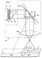
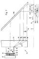
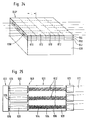
- the first simplest exemplary embodiment of a device according to the invention for generating an image 12 on an image surface 14 - for example a projection surface, on which the image is generated so as to be recognizable to a human eye - comprises a large number of semiconductor emitters 20 arranged in a row of lights 16 along a longitudinal direction 18 of the row of lights 16, each of which can be controlled individually by a common control 22 via individual control lines 24.
- the longitudinal direction 18 extends transversely to an optical axis 26 of a projection optical system, designated as a whole by 28, which images an exit spot 30 of each semiconductor emitter 20, from which radiation 32 generated by it emits, onto an image spot 34 of the image area 14, which is different from that Semiconductor emitter 20 generated radiation is then illuminated.
- the projection optics 28 is constructed in such a way that the exit spot 30 of each semiconductor emitter 20 is projected onto a single image spot 34 in the image area 14 at a specific point in time.
- the projection optics 28, as shown schematically in FIGS. 1 and 2 comprise a tilting mirror 28a, which can be pivoted about a tilting axis 28c by a pivoting drive 28b, and a lens 28d, which emits radiation 32 emerging from each semiconductor emitter 20 with a slight divergence illuminates the image spot 34 on the basis of the geometric image, the image spot 34 generally having an area which corresponds to a multiple of the exit spot 30.
- the image curvature is corrected either via a suitably shaped lens 28d or via a suitably controlled movement of the mirror in such a way that it does not fluctuate about the fixed tilt axis 28c, but rather the tilt axis also moves.
- the row of lights 16 consists of individual semiconductor emitters 30 arranged side by side in the longitudinal direction 18 and the projection optics 28 comprise the tilting mirror 28a and the simple lens 28d
- individual image spots 34 which lie side by side in a longitudinal direction 36 are formed on the image surface 14 form a total of a series of images 38.
- the projection optics 28 are preferably designed such that the individual image spots 34 of the image row 38 do not overlap in the direction of the longitudinal direction 36.
- An embodiment of the projection plane is particularly preferred, in which the image spots 34 follow one another or adjoin one another with their outer edges at a small distance A.
- image row 38 is composed of several sets 38S of adjacent image spots 34, the image spots in each set 38S immediately following one another and sets 38S in longitudinal direction 36 likewise immediately following one another , so that the adjacent image spots 34 of successive sets 38S are also at a distance A from one another, like adjacent image spots 34 within one of the sets 38S.
- the totality of the sets 38S of the image spots 34 thus results in the totality of the image spots 34 of the image row 38.
- the tilting mirror 28a can be tilted into different positions, so that, as shown for example in FIG. 1 with the solid position of the tilting mirror 28a, the set 38S1 of image spots 34 can be generated and following this, as shown in FIG. 1 by the broken line position of the tilting mirror 28a, the adjoining set 38S2.
- a corresponding tilting of the tilting mirror 28a about the tilting axis 28c is to be carried out by means of the swivel drive 28b, the swivel drive 28b being designed in such a way that after illumination of the image spots belonging to the set 38S1, it swivels rapidly into the position shown in broken lines for a time Ta1, while during the time Ta2, which is the same as the time Ta1 to illuminate the image spots 34 of the set 38S2.
- an image row 38 is constructed, for example, from ten sets 38S of image spots 34 and thus the tilting mirror 28a can also be pivoted into ten different positions, each of the sets 38S of image spots 34 being illuminated during the time period Ta, which is for all sentences 38S is the same size.
- an image row 38 of 1250 image spots 34 can be built up in that the light row 16 illuminates 10 adjacent sets 38S of image spots 34 in succession during an image construction cycle, the image construction cycles being repeated periodically.
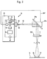
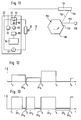
- the controller 22 In order to vary the brightness of the image spots 34 for the human eye observing the image 12, the controller 22, as shown in FIG. 2, comprises a current source 40 which is common to all semiconductor emitters 20 and which is used for each semiconductor emitter 20 provided current control block 42, which includes, for example, an FET transistor 44 as a current-controlling element, to the gate of which a capacitor 46 is connected as a memory element.
- This capacitor 46 of each current control block 42 can be charged with a specific charge via a control switch 48, the charge in the capacitor 46 determining the current through the FET transistor 44.
- the charge to be stored in the capacitor 46 is read out from a buffer 50 for each capacitor 46 of each current control block 42 by triggering the control switch 48 from the buffer 50, the buffer 50 preferably storing all control parameters and by triggering the control switch 48 all control parameters simultaneously the capacitors 46 of all current control blocks 42 are read.
- a trigger block 52 is provided for triggering the control switch 48.
- the buffer memory 50 has the current control parameters for the entire semiconductor emitter 20 the light row 16 has saved.
- the intensity of the radiation 32 emitted by it at the activation time t 1 by correspondingly charging the capacitor 46 of the corresponding one Control blocks 42 are set. The charge is then retained in the capacitor 46 so that the intensity of the radiation from the semiconductor emitter remains constant until the next activation time t 2. If the charge in the capacitor 46 is reduced at this time, this intensity is also maintained until the next activation time t 3. At the activation time t3, for example, the maximum intensity and thus the maximum charge is stored in the capacitor 46, while at the activation time t4 the minimum charge is stored, so that the semiconductor emitter 20 does not emit any radiation or radiation with the intensity 0 between the activation time t4 and t5.
- each individual semiconductor emitter 20 of the light row 16 can now be controlled individually, so that the image row 38 has image spots 34 of different intensities.
- the trigger block 52 is connected on the one hand via a line 56 to the swivel drive 28 and so synchronized with the swivel drive that, for example, at the time t 1 all capacitors 46 for all control blocks 42 are loaded with the values required for illuminating all the image spots 34 of the set 38S1 are and at time t2 the capacitors 46 are loaded so that they store the values for the image spots 34 of the set 38S2.
- the swivel drive 28b carries out the swivel movement from the solid position in FIG. 1 to the dash-dotted position at the greatest possible speed at the actuation time t 2.
- the time period Ta during which all the image spots 34 of the set 38S1 are illuminated in accordance with the brightness values stored in the image generator 54 thus corresponds to the time period between t 1 and t 2.
- This process is repeated during an image construction cycle until all sets 38S of image spots 34 of the image series 38 have been illuminated in succession during the period T a .
- control 22 In an alternative exemplary embodiment of the control 22 'according to the invention, shown in FIG. 4, those components which are identical to the control 22 are provided with the same reference numerals, so that the description of the control 22 is referred to in full in terms of its description.
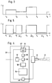
- each control block 42 ′ only comprises the control transistor 44, the gate of which is controlled by a pulse shaping stage 60 and which is only switched on and off between the state.
- the pulse shaper stage in turn stores the control parameters transmitted at the respective control time t and forms a control pulse of different lengths for the control transistor 44 according to the principle of pulse width modulation in accordance with the control parameters, so that the semiconductor emitter 20 is either switched on or off, but with a different length of time between the respective control times t, as shown in Fig. 5.
- the constant power values between the control points t1, t2, t3 and t4 are realized by pulse durations ⁇ t1, ⁇ t2, ⁇ t3 of different lengths, the semiconductor emitter emitting radiation 32 with the maximum power during the pulse durations ⁇ t1, ⁇ t2 and ⁇ t3.
- the effect is exploited that the human eye takes a temporal averaging when viewing the image spot 34 and thus the different pulse widths ⁇ t1, ⁇ t2 and ⁇ t3 convey the impression in the human eye, as if the power values shown in Fig. 3 during the entire period would exist between the control times t1, t2, t3 and t4.
- control 22 ′ is constructed identically to the control 22.
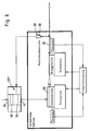
- a third exemplary embodiment of a controller 22 ′′ according to the invention, shown in FIG. 6, is constructed in such a way that each current control block converts the current of the respective semiconductor emitter 20 to the setpoint value stored in the intermediate memory 50 for each set 38S by means of a control circuit 56 regulates during the intended illumination time period Ta, the control circuit 56 measuring the amount of light of the radiation 32 emitted by each semiconductor emitter 20 via monitor photodiodes 60 combined into a monitor photodiode row 58 and driving the respective semiconductor emitter 20 in accordance with the measured value.
- the semiconductor emitter 20 can be driven with variable current, as shown in FIG. 3, so that the control circuit 56 regulates the magnitude of the current for each semiconductor emitter 20, or it is provided that the control circuit 56 regulates the time period ⁇ t while which each semiconductor emitter 20 is supplied with maximum current, the control circuit 56 switching off the current to the respective semiconductor emitter 20 when the quantity of light specified as the desired value in the buffer memory 50 is reached.
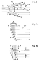
- the projection optics 28 comprise a spreading optics 70 which bring the radiation 32 from the semiconductor emitters to a greater distance, which in the simplest case, as shown in FIG. 7, comprises a substrate material 72 with a Refractive index n1, in which waveguides 74 are introduced, which have a refractive index n2, which is greater than n1.
- the radiation 32 coming from the respective exit spots 30 of the individual semiconductor emitters 20 is coupled into each of these waveguide tracks 74 in the region of one end 76 and is guided to a second end 78, from which the radiation 32 then emerges again.
- the first ends 76 of the waveguide tracks 74 lie at intervals which correspond to the distance between the exit spots 30 of the individual semiconductor emitters 20, so that the radiation 32 emerging from the exit spots 30 in the region of the first ends 76 into the waveguide tracks 74 enters and is guided from these to the second ends 78, which have exit spots 80 for the radiation 32, which are at an image spot spacing BR from one another.
- the radiation 32 emerging from the spreading optics 70 is then in turn imaged by the tilting mirror 28a onto the image row 38 in the image area 14, successive semiconductor emitters 20 being associated with individual image spots 34 in a position of the tilting mirror 28a, the spacing of which is a multiple of the distance A of the image spots 34 of the image series is 38.
- the image spots 34 illuminated by the light row 16 in a position of the tilting mirror 28a thereby form an image spot raster 38R, the same number of image spots 34 lying between individual image spots 34R1 of the image spot raster 38R1.
- the image spot grid 38R1 extends over the entire extent of the image row 38 in the longitudinal direction 36.
- the semiconductor emitter 20 which was previously assigned to one of the image spots 34R1, is assigned to the adjacent image spot 34R2, with the image spot 34R2 lying next to the image spots 34R1 of the image spot pattern 38R1 being assigned to each of the image spots 34R2
- Image spot grid 38R2 is formed whose image spots 34R2 in image row 38 are the image spots following image spots 34R1 of image spot screen 38R1.
- the semiconductor emitters 20 of the light row 16 are assigned to the adjacent image spots 34 to form an image spot grid 38R3, etc., until all the image spots 34 of the image row 38 were once part of an image spot grid 38R.
- the image construction cycle also takes that long, after which all image spots 34 of the image row 38 can be illuminated due to the comb-like assignment of individual image spots to a respective image spot grid and the advancement of the image spot grid to respectively adjacent image spots.
- the image construction cycles are repeated periodically in the same way as described in connection with the first exemplary embodiment of the device according to the invention, the tilt angles by which the tilt mirror 28a is to be pivoted being significantly smaller in this exemplary embodiment than in the first exemplary embodiment.
- a further exemplary embodiment of a spreading optics 70 'according to the invention, shown in detail in FIG. 8, comprises a multiplicity of prism elements 82, 84, wherein for example the prism element 82 is a prism element which is passed through unchanged by the radiation 32 and which is arranged coaxially to the optical axis 26, while the prism elements 84a, b, etc.
- the radiation 32 coming from the semiconductor emitters 20 is reflected by a reflection grating 90 which has reflection surfaces 92 which are at a distance in the direction of incidence 94 of the radiation 32 coming from the semiconductor emitters , which corresponds to the image spot spacing BR and has a distance perpendicular to the direction of incidence 94, which corresponds to the distance between the exit spots 30 of the semiconductor emitters, so that the radiation 32 coming from the exit spots 30 hits the reflection surfaces 92 directly and from them as radiation 32 with the desired Image spot spacing BR is reflected.
- a reflection grating 90 which has reflection surfaces 92 which are at a distance in the direction of incidence 94 of the radiation 32 coming from the semiconductor emitters , which corresponds to the image spot spacing BR and has a distance perpendicular to the direction of incidence 94, which corresponds to the distance between the exit spots 30 of the semiconductor emitters, so that the radiation 32 coming from the exit spots 30 hits the reflection surfaces 92 directly and from them as radiation 32 with the desired Image spot spacing BR is reflected.
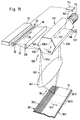
- the projection optics designated as a whole by 128, comprises, in addition to the elements described in connection with the first exemplary embodiment, such as tilting mirror 28a and pivoting drive 28b, a polygon mirror 130, which is arranged around a axis 132 parallel to the longitudinal direction 18 is driven in rotation by a drive 134.
- the polygon mirror 130 in turn has a multiplicity of polygon surfaces 136 arranged at equal angular intervals around the axis 132, one of the polygon surfaces 136 serving as a reflection surface.
- the row of lights 16 comprises a multiplicity of semiconductor emitters 20 which are arranged in succession in the longitudinal direction 18 and are likewise controlled by a control 22, 22 'or 22' '.
- the radiation 32 emerging from the exit spots 30 is first focused by a first focusing optics 138 on the polygon surface 136 in the reflecting position, and the radiation 140 reflected by the polygon surface 136 in the reflecting position is reflected by the tilting mirror 28a, intermediate focused and by a second focusing optics 142 the image area 14 is shown.
- the polygon surface 136 standing in the reflection position rotates about the axis 132 for as long as it is illuminated by the radiation 32, not only does an image row 38 arise on the image area 14, but a plurality of image rows 38 'are created which are arranged side by side in a transverse direction 144 running perpendicular to the longitudinal direction 36.
- a first row of images 38a ' is generated on the image surface 14 when the polygon surface 136 standing in the reflection position is acted upon by the radiation 32 at its foremost region 136a in the direction of rotation 146, and the last row of images 38b' is generated when the one standing in the reflection position Polygon surface 136 with its rearmost area 136b in the direction of rotation 146 of the polygon mirror is acted upon by radiation 32.
- each set of image spots 38S is initially imaged on all rows 38 ', that is to say from row 38a' to row 38b 'by one of the polygon surfaces 136.
- the tilting mirror 28a has moved so far that it illuminates the next image spot set 38S in all image rows 38 ', for example the image spot set 38S2 and maintains this illumination until it is now in Polygon surface 136 standing in the reflection position has projected this image spot set onto all image rows 38 '.
- the tilting mirror 28a has also moved on again, so that now the projection of the next set of image spots 38S3 onto the image rows 38 'takes place.
- the synchronization of the rotating polygon mirror 130 is also carried out with the respective control 22, 22 'or 22''via the connection to the trigger block 52, the tilting movement of the tilting mirror 28a being synchronized with the rotating movement of the polygon mirror 130 such that the tilting mirror 28a Maps row 16 of light to the next following set of image spots when the next following polygon surface 136 is in the reflection position.
- the drive 134 of the polygon mirror is preferably provided with an angle decoder and at the same time the swivel drive 28b of the tilting mirror 28a, so that simple synchronization via the respective control 22, 22 'or 22''is possible (FIG. 11).
- the tilting mirror 28a is driven by the swivel drive 28b in such a way that it quickly changes from one position to the other and this change takes approximately the same time as the change from one polygon surface to the next, so that the dead time is as short as possible.
- the time intervals in which the tilting mirror 28a moves and changes from one set to another are, for example for 125 semiconductor emitters and 100 image build-up cycles per second and 1250 image spots per image row, a maximum of 1 os, during which the polygon mirror 130 with a polygon area then forms a maximum of 1 os 136 each a set of image spots on all image rows 38 '.
- a further semiconductor emitter 148 is provided, as shown in FIG. 11, which illuminates, for example, the polygon surface 136 opposite the polygon surface 136 in the reflection position, the reflected radiation 152 being emitted strikes a detector designated as a whole by 154, which has one detector region 156 or a plurality of detector regions 156, the detector regions 156 having an extent which approximately corresponds to the cross section of the reflected radiation 152, so that when the reflected radiation 152 strikes the respective detector region 156 a precise angular position of the polygon mirror 130 is determined.
- the first detector region 156 is positioned such that when the reflected radiation 152 strikes it, the polygon surface 136 in the reflection position images the exit spots 30 of the semiconductor emitters 20 of the light row 16 in the respective image spot set 38S on the first image row 38a '.
- the second detector surface 156 is preferably arranged such that when the reflected radiation 152 strikes it, the polygon surface 136 in the reflection position images the exit spots 30 of the semiconductor emitters 20 of the light row 16 on the second image row 38 'and so on.
- the impact of the reflected radiation 152 on one of the detector areas 156 generates a signal in the detector 154, which is fed to the trigger block 52, for example, and causes the latter to trigger the control switch 48, if necessary with a corresponding time offset, so that at these control times t the control parameters for everyone Current control block 42 can be changed. It is thus possible to project image spots 34 with different intensity distribution onto each image line 38 'and thus to build up on the image area 14 a two-dimensional image extending in the longitudinal direction 36 and transverse direction 144 from the individual image spots 34 of the image row 38'.
- the control instants t are synchronized with the rotation of the polygon mirror 130 such that they preferably coincide with the instants in which the radiation 32 would strike an edge 160 lying between two polygon surfaces 136.
- the semiconductor emitters 20 can be switched off shortly before the respective activation time t by the fact that the maximum pulse width ⁇ t is shorter by the amount ⁇ t k than the period between successive activation times t, which preferably follow one another at constant time intervals.
- the drive 134 continuously rotates the polygon mirror 130 at a substantially stabilized speed.
- a stepper motor as drive 134 which can be brought into individual rotational positions in a controlled manner and thus does not rotate the polygon mirror 130 continuously, but rather rotates in such rotational positions that the polygon surface 136 in the reflection position successively has different angular positions with respect to the radiation 32 occupies, each individual angular position corresponding to the reflection of the exit spots 30 of the light row 16 in one of the picture rows 38 'and thus the picture rows 38' are illuminated for a defined time and then the polygon surface 136 standing in the reflecting position "jumps" into the next rotational position.
- a stepper motor as drive 134 which can be brought into individual rotational positions in a controlled manner and thus does not rotate the polygon mirror 130 continuously, but rather rotates in such rotational positions that the polygon surface 136 in the reflection position successively has different angular positions with respect to the radiation 32 occupies, each individual angular position corresponding to the reflection of the exit spots 30 of the light row 16 in one of the picture rows 38 'and thus the picture rows 38' are illuminate
- the trigger block 52 can then also be controlled in accordance with the control of the stepping motor, so that the detection of the rotational position of the polygon mirror 130 by means of the detector 154 can be dispensed with.
- a fourth exemplary embodiment of the device according to the invention, shown in FIG. 14, is based on the second exemplary embodiment and provides projection optics 128 which are designed in the same way as in the third exemplary embodiment, so that the spread optics 70 spread over the image spot spacing BR Radiation 32 now hits the tilting mirror 28a in the same way as in the second exemplary embodiment and illuminates the image spots 34 in each of the image rows 38 ', which are encompassed by the respective image spot grid 38R.
- one and the same image spot grid 38R is generated by the rotating polygon mirror 130 in all image rows 38 'and then to the next image spot screen 38R and this in turn in all image rows 38', that is to say from the image row 38a 'to Image series 38b '.
- the tilting mirror 28a can remain standing and, after the generation of the same image spot grid 38R in each of the image rows 38 ', can jump to the next tilt position in order to generate the next subsequent image spot grid 38R in all image rows 38', but it is also possible to slow the tilting mirror 28a to be pivoted continuously such that after one and the same image spot grid 38R has been generated in all image rows 38 ', the tilt is so large that the next image spot grid is already generated in the first image row 38a'.
- corresponding image spots 34 in the successive image rows 38 'do not lie on a straight line which is perpendicular to the longitudinal direction 36, but on a straight line which is at an angle ⁇ 90 ° to the longitudinal direction 36, the oblique position of the corresponding ones
- the time period for imaging each image spot raster 38R on all image rows 38 ' is a maximum of 1 ° s and then the system switches to the next image spot raster 38R.
- the tilting mirror 28a can be omitted if the polygon mirror 130 'does not have polygon surfaces 136' running parallel to the axis 132 ', but, as in Fig 16, all polygon areas 136 'successive to a first polygon area 136e' up to the last polygon area 136l ', to which the first polygon area 136e' is connected again, successively an inclination which changes by a constant angle value from polygon area 136 'to polygon area 136' have their center line 137 with respect to a parallel 133 to the axis 132, so that these polygon surfaces 136 ', each having a different inclination with respect to the axis 132, also take over the function of the tilting mirror 28a.
- the first polygon surface 136e ' is then in the reflection position when the light row 16 is to illuminate the image spot set 38S of the first image row 38a'. As long as the first reflection surface 136e 'is in the reflection position, the image spots 34 of the first image spot set 38S are generated in all image rows 38'.
- next polygon area 136 ' which is inclined so that it illuminates the third set of image spots 38S3 in direct connection to the second set of image spots 38S2.
- a sixth embodiment represents a further development of the fourth embodiment, but also with projection optics 128 ′ with a polygon mirror according to FIG. 17.
- the angles of the polygon surfaces 136 ' which change from polygon surface 136' to polygon surface 136 'are smaller with respect to axis 132, since when changing from the first image spot grid 38R1 to the second image spot grid 38R2, only one deviation has to occur such that in each case from the already generated image spots 34 to the next adjacent image spots 34 in each image row 38 ', while in the fifth embodiment the second image spot set 38S2 has to be shifted by a distance compared to the first image spot set 38S1, which multiplies the number of image spots in one image spot set 38S corresponds to the distance of the image spots A, while the shift in the sixth embodiment only has to be done by the distance of the image spots A.
- each row of lights 16 it is provided for each row of lights 16 that individual semiconductor emitters 20 sit next to one another in the longitudinal direction 18 and thus the row of lights 16 is formed by a single row of semiconductor emitters 20.
- each light row 216 has three rows 218, 220 and 222 of semiconductor emitters 20 which run parallel to one another, the row 218 being composed of semiconductor emitters 20R that emit red light, the row 220 is composed of semiconductor emitters 20G that emit green light, and the row 222 is composed of semiconductor emitters 20B that emit blue light.
- the projection optics 228 are constructed such that a respective semiconductor emitter 20R, a semiconductor emitter 20G and a semiconductor emitter 20B illuminate an image spot 234, in the simplest case it being provided that the partial image spots 236B, 236G and 20B generated by each of the semiconductor emitters 20R, 20G and 236R do not lie congruently one above the other, but do not overlap or only partially overlap, for example.
- a projection optics 228 intermediate focusing of the radiation 32 onto the polygon mirror 130 by means of the first focusing optics 138 can be dispensed with.
- the projection optics 228 are configured identically to the projection optics 128 of the fifth or sixth exemplary embodiment, so that reference is made here to details.
- the rows 218, 220 and 222 of the semiconductor emitters 20R, 20G and 20B are also controlled analogously to the options described in connection with the first exemplary embodiment, but for each of the Rows 218, 220 and 222 a buffer 50 and for each semiconductor emitter 20 a current control block 42 is required, but the control is carried out in such a way that at a control time t the control parameters for the semiconductor emitters 20R, 20G and 20B of all three rows 218, 220 and 222 simultaneously can be read from the buffer.
- the wavelengths of the semiconductor emitters 20R, 20G and 20B and the possible maximum intensities are selected such that all colors, in particular white, can be generated by color mixing in the image spots 234 for the human eye.
- the image generator 54 now generates three control parameters for each image spot 234 for each of the semiconductor emitters 20R, 20G and 20B illuminating this image spot 234.
- the three rows 218, 220 and 222 each comprising the semiconductor emitters 20R, 20G and 20B, are also provided. The control of the same takes place as described in connection with the third embodiment.
- the projection optics 328 between the light row 216 and the polygon mirror 130 each comprise two sets of mirrors 330 and 332 in order to combine the radiation 32R from the semiconductor emitters 20R, the radiation 32G from the semiconductor emitters 20G and the radiation 32B from the semiconductor emitters 20B.
- the first set of mirrors 330 comprises a dichroic mirror 333 arranged in the beam path of the radiation 32R and a mirror 336 reflecting the radiation 32G on the dichroic mirror.
- the second set of mirrors 332 comprises a dichroic mirror 338 arranged in the beam path of the radiation 32R and one the radiation 32B on the dichroic mirror 338 reflective mirror 340.
- the two dichroic mirrors 333 and 338 thus combine the radiation 32R, 32G and 32B to form radiation 32V, which impinges on the polygon mirror 130 designed in accordance with the fifth or sixth exemplary embodiment and by the latter in the manner already described in connection with the second exemplary embodiment Image area 14 is reflected.
- the advantage of this projection optics 328 can be seen in the fact that, in this exemplary embodiment, the partial image spots 336, produced by imaging the exit spots 30 of the semiconductor emitters 20R, 20G and 20B, can be superimposed essentially congruently in each image spot 334.
- the semiconductor emitters preferably comprise semiconductor lasers designed as so-called edge emitters, as shown schematically in FIG. 20.
- Such edge emitters consist of a multiplicity of semiconductor layers 800, between which a laser-active layer 802 is arranged.
- the laser radiation 806 emerges from this laser-active layer in the region of an exit spot 804.
- Such an edge emitter is operated by supplying current via two current connections 808 and 810, the current flowing essentially perpendicular to the layers 800 and 802.
- Embodiments of such edge emitters can be found in the magazine Laser Focus World, July 1993, Vol. 29, No. 7, pages 83 to 92 described in detail.
- edge emitters can be seen in the fact that they can be produced in a simple manner side by side as a so-called array on a substrate.
- edge emitters it is possible to provide semiconductor lasers in the form of so-called vertical emitters, shown in FIG. 21, as radiation sources, with such vertical emitters also having a laser-active layer 902 between a plurality of semiconductor layers 900 and additional laser-active layer 902 on both sides , Layers 904 serving as Bragg reflectors are provided.
- the resulting laser radiation does not propagate parallel to the active layer 802 as in the case of the edge emitter, but perpendicular to the active layer 902, passes through the substrate 910 and preferably exits perpendicular to the plane of the substrate 910.
- Vertical emitters have the advantage that the resulting laser radiation 906 has an approximately circular cross section and can therefore be coupled to other optical elements, for example fiber-optic elements, in a simple manner.
- the following laser materials are preferably used as laser materials for the generation of radiation in the visible range with different colors: Al x Ga y In 1-xy P on GaAs for 610-690 nm red Zn 1-x Mg x S 1-y Se y on GaAs for 450-550 nm blue green Al x Ga y In 1-xy N For UV - red
- Such materials would be, for example A1 x Ga 1-x As on GaAs (780-880nm) for blue In x Ga 1-x As on GaAs (880-1100nm) for blue, green In 1-x Ga x As y P 1-y on InP (1100-1600nm) for red.
- An embodiment of such semiconductor emitters 20 'doubling the wavelength of the radiation from the radiation source, shown in FIGS. 22 and 23 in the form of a section from the light row 820, comprises an array 822 of edge emitters 826 arranged on a common substrate 824, which are characterized by special emitters laser-active layers arranged on the common substrate 824 are formed6 and each have as laser-active layer 802 a strip-shaped region 828 of a continuous layer 830 arranged on the common substrate 824.
- Each of the semiconductor lasers 826 serving as a radiation source is assigned a frequency doubler 832, each of which comprises a waveguide structure 834 in which a frequency-doubled medium is arranged as a waveguide channel 836.
- the waveguide structure 834 guides the radiation generated by the respective semiconductor laser 826 in such a narrow cross section that a power density of at least 105W / cm2, preferably at least 106W / cm2, which is required for efficient frequency doubling in the frequency-doubling medium, is achieved.
- all frequency doublers 832 are also arranged on a common substrate 838 in the form of an array 840.
- the waveguide structure 834 is formed by a base layer 842 and a cover layer 844, which represent upper and lower walls of the waveguide channel 834, and spaced-apart strip areas 846 and 848 of an intermediate layer 850, which form side walls of the waveguide channel 834 and a strip area 852 des Include the intermediate layer 850 between them, which forms the frequency doubling medium 836 serving as the waveguide core.
- the base layer 842, the top layer 844 and the strip-shaped regions 846 and 848 of the intermediate layer 850 have a refractive index which is smaller than the refractive index of the strip-shaped region 852, so that at the boundaries between the strip-shaped region 852 and the layers 842 and 844 as well the strip-shaped regions 846 and 848 there is a total reflection of the radiation and thus the guidance of the radiation in the waveguide structure 834.
- the extension of the waveguide structures 834 transverse to their longitudinal direction 854 is expediently chosen to be approximately the same size as the extension of the laser-active regions 828 in the direction of propagation 856 of the laser radiation.
- the fundamental wave that is to say the radiation coming from the corresponding semiconductor laser 826
- the doubled radiation must remain in phase the entire way through the frequency doubling medium. This is optimally achieved when working with an uncritical or non-critical phase adjustment in which the angle is 0 or 90 °.
- the respective material is preferably adapted to the corresponding wavelength by varying the temperature, so that, for example, the substrate 838 is seated on a temperature control device 860, with which the entire array 840 of frequency doublers 832 can be brought to an optimum temperature for the uncritical phase adjustment this is durable.
- the temperature control device 860 is preferably provided with a control, by means of which a predeterminable temperature can be set and maintained by readjustment.
- the direction of the crystal in the frequency-doubling medium 836 is expediently predetermined by the orientation of the substrate 838, which is oriented such that the optical axis of the substrate is oriented in the desired direction to the longitudinal direction 854 of the waveguide channel 834. If the layers 842, 844 and 850 made of the same base material, possibly with different dopings, are grown on this substrate 838, these layers have the same orientation of the optical axes as the substrate 838 and consequently the position of the optical axes is also frequency doubling Medium 836 can be specified.
- phase adaptation is achieved in that in the frequency-doubling medium 836' domains 870 and 872 follow one another, in which the non-linear ones Coefficients of the frequency doubling medium 836 each have opposite signs.
- An extension L of the domains 870 and 872 in the longitudinal direction 854 of the waveguide channels 834 is to be coordinated in such a way that it corresponds to the coherence length.
- the array 840 ' is of the same design as the array 840, so that full reference can be made to the explanations in this regard and the same reference numerals are used for the same elements.
- a crystal of lithium niobate for the wavelengths green and red is preferably used as the frequency-doubling medium and a crystal of potassium niobate for the wavelength blue.
- the waveguide structure 834 is produced in that the material surrounding the waveguide core is lithium niobate or potassium niobate, which has additionally been doped with magnesium or other elements which lower the refractive index.
- an array 922 of semiconductor lasers 926 designed as vertical emitters is used.
- the radiation 928 from these semiconductor emitters is focused by focusing elements 930 onto frequency doublers 932, which are likewise arranged in an array 940 on a common substrate and are constructed and constructed in the same way as the array 840, so that reference can be made in full to the explanations in this regard .
- the focusing optics 930 are not designed as lens optics, but rather as gradient index lenses, which are used as a block between the respective semiconductor lasers 926 and the corresponding frequency doublers 932 and, due to the gradient index, focus the radiation 928 onto the waveguide channels 934.
- the end of the frequency doubler 932 expansion optics 970 are preferably arranged, which are also gradient index lenses that generate a substantially parallel beam 972.
- an array 1022 of individual semiconductor lasers 1026 designed as edge emitters is arranged on the common substrate 1024, individual laser-active layers being formed on the common substrate 1024, each as laser-active layer 1002 have a strip-shaped area on a continuous layer arranged on the common substrate 1024.
- the substrate 1024 sits on a cooling element 1050 and is thermally coupled to a temperature sensor 1052, which regulates the cooling element 1050 to a constant temperature via a temperature control 1054, so that ultimately the substrate 1024 of the semiconductor emitter 1026 also has a constant temperature.
- a cooling element 1056 is provided for the frequency doubler 1032, the base layer 1042 being cooled by the cooling element 1056. Furthermore, a temperature sensor 1058 is coupled to this base layer 1042, which also again enables the temperature control 1054 to set a constant temperature of the base layer 1042, so that ultimately a constant temperature for the frequency-doubling medium 1036 is also present in the waveguide channel.
- the exit spots 1060 of the edge emitters 1026 are preferably imaged via a lens system 1062 onto the entrance spots 1064 of the waveguide structure and their exit spots 1066 are in turn shaped via a lens system 1068 into parallel radiation 32 leaving the respective semiconductor emitter 1020, the radiation being a window 1070 of a housing 1072 penetrates, which in turn includes both the array 1022 and the entirety of the waveguide structures 1034 with the cooling elements 1050 and 1056 and the temperature sensors 1052 and 1058 and the lenses 1062 and 1066.
- a beam splitter 1074 is provided in front of the exit window 1070, which reflects part of the radiation passing through the outer window 1070 onto a row of monitor photodiodes 1076, which is likewise arranged in the housing 1072 and has a monitor photodiode for each of the edge emitters 1026. All monitor photodiodes are coupled to the controller 22 ', which has already been described in detail in connection with the third exemplary embodiment of the controller according to the invention according to FIG. 6.
- the lens systems 1062 and 1068 each comprise the radiation-forming microlens systems, which are likewise arranged on a substrate. Furthermore, the waveguide structure of the frequency doubler 1032 is again shown enlarged in FIG. 27.
Landscapes
- Physics & Mathematics (AREA)
- Optics & Photonics (AREA)
- Engineering & Computer Science (AREA)
- Multimedia (AREA)
- Signal Processing (AREA)
- Mechanical Optical Scanning Systems (AREA)
- Led Device Packages (AREA)
- Led Devices (AREA)
- Devices For Indicating Variable Information By Combining Individual Elements (AREA)
- Control Of Indicators Other Than Cathode Ray Tubes (AREA)
- Projection Apparatus (AREA)
Applications Claiming Priority (2)
| Application Number | Priority Date | Filing Date | Title |
|---|---|---|---|
| DE4428202 | 1994-08-09 | ||
| DE4428202A DE4428202A1 (de) | 1994-08-09 | 1994-08-09 | Vorrichtung zur Erzeugung eines Bildes |
Publications (3)
| Publication Number | Publication Date |
|---|---|
| EP0696875A2 true EP0696875A2 (fr) | 1996-02-14 |
| EP0696875A3 EP0696875A3 (fr) | 1998-04-08 |
| EP0696875B1 EP0696875B1 (fr) | 2001-11-14 |
Family
ID=6525274
Family Applications (1)
| Application Number | Title | Priority Date | Filing Date |
|---|---|---|---|
| EP95111811A Expired - Lifetime EP0696875B1 (fr) | 1994-08-09 | 1995-07-27 | Dispositif pour produire une image |
Country Status (4)
| Country | Link |
|---|---|
| US (1) | US5818546A (fr) |
| EP (1) | EP0696875B1 (fr) |
| JP (1) | JP2779337B2 (fr) |
| DE (2) | DE4428202A1 (fr) |
Cited By (6)
| Publication number | Priority date | Publication date | Assignee | Title |
|---|---|---|---|---|
| WO1998024240A1 (fr) * | 1996-11-27 | 1998-06-04 | Laser Power Corporation | Systeme d'affichage a balayage par faisceaux laser multiples |
| WO1998047035A1 (fr) * | 1997-04-11 | 1998-10-22 | Bootsman Holding B.V. | Systeme de deplacement d'un faisceau laser, par exemple systeme de marquage au laser |
| US5990983A (en) * | 1994-09-30 | 1999-11-23 | Laser Power Corporation | High resolution image projection system and method employing lasers |
| US6154259A (en) * | 1996-11-27 | 2000-11-28 | Photera Technologies, Inc. | Multi-beam laser scanning display system with speckle elimination |
| US6351324B1 (en) | 2000-03-09 | 2002-02-26 | Photera Technologies, Inc. | Laser imaging system with progressive multi-beam scan architecture |
| CN111338161A (zh) * | 2018-12-18 | 2020-06-26 | 深圳光峰科技股份有限公司 | 投影装置 |
Families Citing this family (17)
| Publication number | Priority date | Publication date | Assignee | Title |
|---|---|---|---|---|
| JPH11289495A (ja) * | 1998-04-03 | 1999-10-19 | Sony Corp | 画像入力装置 |
| DE19912654A1 (de) * | 1999-03-20 | 2000-05-25 | Agfa Gevaert Ag | Vorrichtung zum Beschreiben von fotografischem Material |
| US6583912B1 (en) * | 1999-04-13 | 2003-06-24 | Koninklijke Philips Electronics N.V. | Display system with light-emitting elements |
| DE19937267A1 (de) * | 1999-08-06 | 2001-02-15 | Baasel Carl Lasertech | Vorrichtung zur Behandlung eines Substrates mittels Laserstrahlung |
| US6567605B1 (en) | 2000-08-25 | 2003-05-20 | The Boeing Company | Fiber optic projection device |
| US7102700B1 (en) * | 2000-09-02 | 2006-09-05 | Magic Lantern Llc | Laser projection system |
| US7230657B2 (en) * | 2002-05-03 | 2007-06-12 | Hewlett-Packard Development Company, L.P. | Light emitting device projection methods and systems |
| US7167216B2 (en) * | 2002-05-03 | 2007-01-23 | Hewlett-Packard Development Company, L.P. | Projection system with adjustable aspect ratio optics |
| US7184104B2 (en) * | 2002-05-03 | 2007-02-27 | Hewlett-Packard Development Company, L.P. | Projector having scanning optics |
| US7148933B2 (en) * | 2002-05-03 | 2006-12-12 | Hewlett-Packard Development Company, L.P. | Projector having alignment optics and electronics |
| US7042483B2 (en) * | 2003-03-10 | 2006-05-09 | Eastman Kodak Company | Apparatus and method for printing using a light emissive array |
| DE102004063832B4 (de) * | 2004-12-29 | 2010-02-11 | Xtreme Technologies Gmbh | Anordnung zur Erzeugung eines gepulsten Laserstrahls hoher Durchschnittsleistung |
| US7287862B2 (en) * | 2005-02-18 | 2007-10-30 | Symbol Technologies, Inc. | Compact image projection module |
| KR100785050B1 (ko) * | 2006-04-21 | 2007-12-12 | 에이치비전자주식회사 | 레이저 디스플레이 장치 |
| US8169454B1 (en) * | 2007-04-06 | 2012-05-01 | Prysm, Inc. | Patterning a surface using pre-objective and post-objective raster scanning systems |
| US20090153811A1 (en) * | 2007-11-11 | 2009-06-18 | Mark Stephen Braiman | Cooperative Pointillistic Projection of a Graphical Image on a Pre-Selected Remote Surface by Using a Multiplicity of Lasers |
| JP5656506B2 (ja) * | 2010-08-17 | 2015-01-21 | 三菱重工業株式会社 | シリンダライナ |
Citations (1)
| Publication number | Priority date | Publication date | Assignee | Title |
|---|---|---|---|---|
| DE2341705A1 (de) | 1972-08-25 | 1974-04-04 | Hitachi Ltd | Bildwiedergabegeraet |
Family Cites Families (12)
| Publication number | Priority date | Publication date | Assignee | Title |
|---|---|---|---|---|
| US4297723A (en) * | 1980-01-28 | 1981-10-27 | The Singer Company | Wide angle laser display system |
| FR2577371B1 (fr) * | 1985-02-12 | 1988-06-24 | Centre Nat Rech Scient | Dispositif de projection d'image de television sur grand ecran |
| US4805012A (en) * | 1987-09-23 | 1989-02-14 | Eastman Kodak Company | System for high resolution exposure address with coarser resolution exposing array |
| JPH02149887A (ja) * | 1988-11-30 | 1990-06-08 | Pioneer Electron Corp | カラー表示装置 |
| US4978202A (en) * | 1989-05-12 | 1990-12-18 | Goldstar Co., Ltd. | Laser scanning system for displaying a three-dimensional color image |
| DE69123288T2 (de) * | 1990-05-21 | 1997-04-24 | Victor Company Of Japan | Anzeigegerät |
| JPH0470711A (ja) * | 1990-07-11 | 1992-03-05 | Canon Inc | レーザ走査光学系 |
| KR950007875B1 (ko) * | 1991-01-30 | 1995-07-20 | 삼성전자주식회사 | 레이저를 이용한 표시장치 |
| DE4130844A1 (de) * | 1991-09-17 | 1993-03-18 | Ronkholz Karl Heinz | Alphanumerische anzeigeeinrichtung |
| JPH05113546A (ja) * | 1991-10-21 | 1993-05-07 | Rohm Co Ltd | 光源ユニツト |
| US5317348A (en) * | 1992-12-01 | 1994-05-31 | Knize Randall J | Full color solid state laser projector system |
| JPH08509067A (ja) * | 1993-02-03 | 1996-09-24 | ナイター | イメージ投射方法及び装置 |
-
1994
- 1994-08-09 DE DE4428202A patent/DE4428202A1/de not_active Ceased
-
1995
- 1995-07-27 DE DE59509828T patent/DE59509828D1/de not_active Expired - Fee Related
- 1995-07-27 EP EP95111811A patent/EP0696875B1/fr not_active Expired - Lifetime
- 1995-08-07 US US08/512,056 patent/US5818546A/en not_active Expired - Fee Related
- 1995-08-09 JP JP20356695A patent/JP2779337B2/ja not_active Expired - Fee Related
Patent Citations (1)
| Publication number | Priority date | Publication date | Assignee | Title |
|---|---|---|---|---|
| DE2341705A1 (de) | 1972-08-25 | 1974-04-04 | Hitachi Ltd | Bildwiedergabegeraet |
Non-Patent Citations (3)
| Title |
|---|
| LASER FOCUS WORLD, vol. 29, no. 7, July 1993 (1993-07-01), pages 83 - 92 |
| OPTICS LETTERS, vol. 18, no. 22, pages 1937 FF |
| SPEKTRUM DER WISSENSCHAFT, January 1992 (1992-01-01), pages 76FF |
Cited By (7)
| Publication number | Priority date | Publication date | Assignee | Title |
|---|---|---|---|---|
| US5990983A (en) * | 1994-09-30 | 1999-11-23 | Laser Power Corporation | High resolution image projection system and method employing lasers |
| WO1998024240A1 (fr) * | 1996-11-27 | 1998-06-04 | Laser Power Corporation | Systeme d'affichage a balayage par faisceaux laser multiples |
| US6154259A (en) * | 1996-11-27 | 2000-11-28 | Photera Technologies, Inc. | Multi-beam laser scanning display system with speckle elimination |
| WO1998047035A1 (fr) * | 1997-04-11 | 1998-10-22 | Bootsman Holding B.V. | Systeme de deplacement d'un faisceau laser, par exemple systeme de marquage au laser |
| US6351324B1 (en) | 2000-03-09 | 2002-02-26 | Photera Technologies, Inc. | Laser imaging system with progressive multi-beam scan architecture |
| CN111338161A (zh) * | 2018-12-18 | 2020-06-26 | 深圳光峰科技股份有限公司 | 投影装置 |
| CN111338161B (zh) * | 2018-12-18 | 2022-04-12 | 深圳光峰科技股份有限公司 | 投影装置 |
Also Published As
| Publication number | Publication date |
|---|---|
| JPH09120036A (ja) | 1997-05-06 |
| DE4428202A1 (de) | 1996-02-15 |
| US5818546A (en) | 1998-10-06 |
| JP2779337B2 (ja) | 1998-07-23 |
| EP0696875B1 (fr) | 2001-11-14 |
| EP0696875A3 (fr) | 1998-04-08 |
| DE59509828D1 (de) | 2001-12-20 |
Similar Documents
| Publication | Publication Date | Title |
|---|---|---|
| EP0683595B1 (fr) | Dispositif de formation d'image | |
| EP0696875B1 (fr) | Dispositif pour produire une image | |
| DE3882691T2 (de) | Video-abbildungssysteme. | |
| DE69519220T2 (de) | Einzeltafel-farbbildprojektionssystem mit verbesserter abtastung | |
| DE69329992T2 (de) | Farbbildprojektor | |
| DE60219258T2 (de) | Beleuchtungssystem und damit versehener Projektor | |
| DE4324848C1 (de) | Videoprojektionssystem | |
| DE69411019T2 (de) | Optische aufzeichnung von daten | |
| DE19841509A1 (de) | Kompakte Großflächen-Laserprojektionsanzeige mit einem Hybrid-Videolaserfarbmischer | |
| DE102013226622A1 (de) | Leuchtvorrichtung mit Leuchtstofffläche | |
| DE19751106A1 (de) | Laserdrucker zum Drucken auf ein lichtempfindliches Medium | |
| EP2095184A2 (fr) | Dispositif de projection ayant une propriété de projection améliorée | |
| EP1196794B1 (fr) | Procédé et dispositif pour produire des hologrammes d'écran | |
| DE60102597T2 (de) | Laser mit hoher spitzenleistung und dessen anwendung zur erzeugung von licht im extrem-uv-bereich | |
| DE3939551A1 (de) | Optisches positionierungssystem fuer mindestens einen bildpunkt | |
| WO2007085242A2 (fr) | Dispositif de projection pour un collimateur de pilotage et procede pour le commander | |
| DE102007025330A1 (de) | Projektionsvorrichtung | |
| WO2000011513A1 (fr) | Dispositif permettant l'affichage volumetrique d'une image 3d par generation de plasma pulse en atmosphere naturelle au moyen d'un faisceau laser focalise | |
| EP0961152A1 (fr) | Procédé et dispositif pour former un faisceau de lumière collimaté à partir des émissions de plusieurs sources de lumière | |
| DE10030417A1 (de) | Bildprojektor | |
| DE102016217323A1 (de) | Lichtmodul zum Bereitstellen von Effektlicht | |
| DE1462404A1 (de) | Vorrichtung zum Empfang eines mehrfarbigen Fernsehbildes | |
| WO2025114134A1 (fr) | Ensemble de projection et procédé d'éclairage d'une pluralité de pixels virtuels | |
| DE102012011202A1 (de) | Projektor und Verfahren zum Erzeugen eines Bildes | |
| DE69721003T2 (de) | Verfahren und Gerät zur Belichtung eines Bildaufzeichnungsmediums |
Legal Events
| Date | Code | Title | Description |
|---|---|---|---|
| PUAI | Public reference made under article 153(3) epc to a published international application that has entered the european phase |
Free format text: ORIGINAL CODE: 0009012 |
|
| AK | Designated contracting states |
Kind code of ref document: A2 Designated state(s): DE FR NL |
|
| PUAL | Search report despatched |
Free format text: ORIGINAL CODE: 0009013 |
|
| RAP1 | Party data changed (applicant data changed or rights of an application transferred) |
Owner name: DEUTSCHES ZENTRUM FUER LUFT- UND RAUMFAHRT E.V. |
|
| RAP3 | Party data changed (applicant data changed or rights of an application transferred) |
Owner name: DEUTSCHES ZENTRUM FUER LUFT- UND RAUMFAHRT E.V. |
|
| AK | Designated contracting states |
Kind code of ref document: A3 Designated state(s): DE FR NL |
|
| 17P | Request for examination filed |
Effective date: 19980923 |
|
| 17Q | First examination report despatched |
Effective date: 19991217 |
|
| GRAG | Despatch of communication of intention to grant |
Free format text: ORIGINAL CODE: EPIDOS AGRA |
|
| GRAG | Despatch of communication of intention to grant |
Free format text: ORIGINAL CODE: EPIDOS AGRA |
|
| GRAH | Despatch of communication of intention to grant a patent |
Free format text: ORIGINAL CODE: EPIDOS IGRA |
|
| GRAH | Despatch of communication of intention to grant a patent |
Free format text: ORIGINAL CODE: EPIDOS IGRA |
|
| GRAA | (expected) grant |
Free format text: ORIGINAL CODE: 0009210 |
|
| AK | Designated contracting states |
Kind code of ref document: B1 Designated state(s): DE FR NL |
|
| REF | Corresponds to: |
Ref document number: 59509828 Country of ref document: DE Date of ref document: 20011220 |
|
| PLBE | No opposition filed within time limit |
Free format text: ORIGINAL CODE: 0009261 |
|
| STAA | Information on the status of an ep patent application or granted ep patent |
Free format text: STATUS: NO OPPOSITION FILED WITHIN TIME LIMIT |
|
| 26N | No opposition filed | ||
| PGFP | Annual fee paid to national office [announced via postgrant information from national office to epo] |
Ref country code: DE Payment date: 20030707 Year of fee payment: 9 |
|
| PGFP | Annual fee paid to national office [announced via postgrant information from national office to epo] |
Ref country code: NL Payment date: 20030721 Year of fee payment: 9 Ref country code: FR Payment date: 20030721 Year of fee payment: 9 |
|
| PG25 | Lapsed in a contracting state [announced via postgrant information from national office to epo] |
Ref country code: NL Free format text: LAPSE BECAUSE OF NON-PAYMENT OF DUE FEES Effective date: 20050201 Ref country code: DE Free format text: LAPSE BECAUSE OF NON-PAYMENT OF DUE FEES Effective date: 20050201 |
|
| PG25 | Lapsed in a contracting state [announced via postgrant information from national office to epo] |
Ref country code: FR Free format text: LAPSE BECAUSE OF NON-PAYMENT OF DUE FEES Effective date: 20050331 |
|
| NLV4 | Nl: lapsed or anulled due to non-payment of the annual fee |
Effective date: 20050201 |
|
| REG | Reference to a national code |
Ref country code: FR Ref legal event code: ST |