EP0697723A2 - Procédé de métallisation d'une couche isolante - Google Patents
Procédé de métallisation d'une couche isolante Download PDFInfo
- Publication number
- EP0697723A2 EP0697723A2 EP95480097A EP95480097A EP0697723A2 EP 0697723 A2 EP0697723 A2 EP 0697723A2 EP 95480097 A EP95480097 A EP 95480097A EP 95480097 A EP95480097 A EP 95480097A EP 0697723 A2 EP0697723 A2 EP 0697723A2
- Authority
- EP
- European Patent Office
- Prior art keywords
- layer
- insulator
- metal
- reflected radiation
- apertures
- Prior art date
- Legal status (The legal status is an assumption and is not a legal conclusion. Google has not performed a legal analysis and makes no representation as to the accuracy of the status listed.)
- Withdrawn
Links
Images



Classifications
-
- H—ELECTRICITY
- H10—SEMICONDUCTOR DEVICES; ELECTRIC SOLID-STATE DEVICES NOT OTHERWISE PROVIDED FOR
- H10W—GENERIC PACKAGES, INTERCONNECTIONS, CONNECTORS OR OTHER CONSTRUCTIONAL DETAILS OF DEVICES COVERED BY CLASS H10
- H10W20/00—Interconnections in chips, wafers or substrates
- H10W20/01—Manufacture or treatment
- H10W20/031—Manufacture or treatment of conductive parts of the interconnections
- H10W20/056—Manufacture or treatment of conductive parts of the interconnections by filling conductive material into holes, grooves or trenches
-
- H—ELECTRICITY
- H10—SEMICONDUCTOR DEVICES; ELECTRIC SOLID-STATE DEVICES NOT OTHERWISE PROVIDED FOR
- H10W—GENERIC PACKAGES, INTERCONNECTIONS, CONNECTORS OR OTHER CONSTRUCTIONAL DETAILS OF DEVICES COVERED BY CLASS H10
- H10W20/00—Interconnections in chips, wafers or substrates
- H10W20/01—Manufacture or treatment
- H10W20/071—Manufacture or treatment of dielectric parts thereof
- H10W20/081—Manufacture or treatment of dielectric parts thereof by forming openings in the dielectric parts
- H10W20/084—Manufacture or treatment of dielectric parts thereof by forming openings in the dielectric parts for dual-damascene structures
- H10W20/088—Manufacture or treatment of dielectric parts thereof by forming openings in the dielectric parts for dual-damascene structures involving partial etching of via holes
-
- H—ELECTRICITY
- H10—SEMICONDUCTOR DEVICES; ELECTRIC SOLID-STATE DEVICES NOT OTHERWISE PROVIDED FOR
- H10W—GENERIC PACKAGES, INTERCONNECTIONS, CONNECTORS OR OTHER CONSTRUCTIONAL DETAILS OF DEVICES COVERED BY CLASS H10
- H10W20/00—Interconnections in chips, wafers or substrates
- H10W20/01—Manufacture or treatment
- H10W20/071—Manufacture or treatment of dielectric parts thereof
- H10W20/081—Manufacture or treatment of dielectric parts thereof by forming openings in the dielectric parts
- H10W20/084—Manufacture or treatment of dielectric parts thereof by forming openings in the dielectric parts for dual-damascene structures
- H10W20/0888—Manufacture or treatment of dielectric parts thereof by forming openings in the dielectric parts for dual-damascene structures wherein via-level dielectrics are compositionally different than trench-level dielectrics
Definitions
- the invention relates to a process for making metal features in an insulator layer for integrated circuit fabrication.
- Photolithography is a fundamental technology in the production of semiconductor devices.
- a photosensitive polymer film is applied to the substrate, dried, and then exposed with the proper geometrical patterns through a photomask. After exposure, the wafer is soaked in a solution that develops the images in the photosensitive material. Depending upon the type of polymer used, either exposed or non-exposed areas of film are removed in the developing process.
- a frequent problem encountered in this process is reflectivity of the activating radiation back into the resist by the substrate, especially by substrates containing highly reflecting, irregular topographies. Such reflectivity tends to cause standing wave ripples and reflective notches, which interfere with the desired pattern in the photoresist.
- the notches are particularly bad when the support or metallurgy is nonplanar.
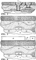
- FIG. 1 depicts a substrate 1 containing numerous structures appropriate to integrated circuit function whose nature and function will be described later.
- the substrate has been covered with an insulator 32 and patterned with a series of channels 7, which will be used for wiring interconnections in semiconductor processing.
- the channels 7 are to be deepened and the insulator layer 32 is to be cut back slightly to create vias, contacts or interconnections between channels.
- a layer of photoresist has been deposited on the insulator 32 and has been exposed and developed. Because of reflected radiation during the exposure step, the development of the photoresist 36 has removed a notch 3 where a straight side was intended.
- the photoresist when used as an etch mask, etching occurs in a region that was to have been protected by the resist.
- the insulator layer 32 appears as shown in FIG. 3 having a portion of the insulator etched away where a vertical wall had been intended.
- the metal 46 When the channel is filled with a suitable metal and planarized, the metal 46 has an extension 5 which intrudes into the region which was supposed to be occupied by insulator. The extension 5 gives rise to shorting and circuit failure, particularly when the dimensions are critical.
- the art discloses three basic approaches to the problem: (1) decrease the intensity or time of exposure to the radiation; (2) incorporate a radiation absorber into the photoresist; and (3) incorporate a dye or other chromophore of appropriate absorption into a removable polymer layer beneath the resist.
- Each of these approaches has its attendant drawbacks: Decreasing the intensity or duration of the exposure decreases reflective radiation but also decreases the radiation necessary for efficient exposure. This becomes an acute problem when creating sub-micron features. The result of underexposure is blocked or partially blocked contact/via openings due to residual resists remaining in the pattern after photodeveloping and subsequent etching. The incorporation of a radiation absorber into the photoresist itself cuts down on reflected radiation but also results in decreased resist sensitivity.
- the radiation absorbing layer beneath the resist has, in the prior art, been of such anature that its removal was required prior to any subsequent deposition of metal. This adds additional steps to the process, and removal of the absorber can affect exposed regions in the contact/via openings.
- invention relates to a process comprising the steps of:
- the apertures will extend through the insulator layer and into the substrate.
- the apertures, when filled and planarized, may become features such as vias and contacts; the channels may become features such as local interconnects.
- the patterning of the insulator and titanium nitride layers will be accomplished by depositing, exposing and developing a photoresist on the titanium nitride layer, etching both the insulator and the titanium nitride layers, and removing the photoresist.
- Preferred metals for the metallization include tungsten, copper, aluminum and molybdenum.
- the invention relates to a process comprising the steps of:
- the apertures will extend through the insulator layer and into the substrate.
- a preferred ARC is tantalum; when the metal is aluminum, a preferred ARC is titanium; and when the metal is tungsten, a preferred ARC is titanium nitride.
- the process of the invention involves the deposition of an anti-reflective coating (ARC) on an insulator layer, patterning of the ARC using a photoresist, etching both the ARC and the insulator, removing the photoresist, and depositing the metal for interconnects, vias, contacts etc. over the ARC to fill the channels and apertures.
- the metal is then planarized back to the insulator, commonly by chemical-mechanical polishing (CMP), to provide a planarized insulator containing the appropriate metallization.
- CMP chemical-mechanical polishing
- the ARC will provide improved adhesion between the metal and insulator so that the resulting structure can be chemical-mechanical polished without pulling the metal out of any of the features.
- titanium nitride has been used as an ARC for the deposition of tungsten; however, the invention is by no means limited to such a combination.
- Other materials that attenuate reflected radiation and that improve adhesion can be used as the ARC as long as they will both survive the deposition of metal without loss of function and not interfere with the subsequent function of the device.
- tantalum as an ARC for copper, titanium as an ARC for aluminum, and titanium nitride as an ARC for tungsten are particularly attractive combinations.
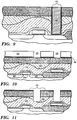
- FIG. 5 shows a typical semiconductor fabrication at the stage of processing wherein a silicon substrate 20 has been provided with two diffusions or doped regions 22 and a conducting layer 24, of polysilicon, which will form a gate electrode in the semiconductor device which is to be formed on the silicon substrate.
- the conducting layer 24 has an electrically insulating layer 26 separating it from substrate 20 and diffusions 22. In the particular embodiment shown, it is the sloping "bird's beak" of the field oxide 25 that gives rise to the reflection problem, but similar problems can arise with shallow trench isolations (STI's) and other reflective features in layers below the resist.
- a layer of boron phosphorous silicate glass 28 and a layer of phosphorous silicate glass 30 have been deposited and reflowed, although for other applications two layers would not be necessary.
- the insulator 32 in this case silicon dioxide, has been deposited by CVD and planarized.
- the titanium nitride anti-reflective coating 34 is conformally deposited.
- a photoresist 36 is laid down on top of the titanium nitride, patterned, and developed to provide a series of openings 38.
- the wafer is etched, in this case by reactive ion etching (RIE) with CHF3 plus C02.
- RIE reactive ion etching
- the etch cuts through the TiN 34 the CVD oxide 32, and the reflowed glass (28 and 30) to the substrate above the diffuson 22.
- the photoresist is then removed, resultin g in a structure shown in FIG. 7.
- a second layer 44 of titanium/titanium nitride is conformally deposited to coat the surface of the existing ARC and the trench structure. This may be conveniently accomplished by sputtering titanium, first using argon as a bombarding species and then introducing nitrogen. (see for example U.S.
- Tungsten 46 is then deposited to completely fill the trench and extend over the titanium nitride layer as shown in FIG. 8.
- the tungsten is CMP planarized to provide the structure shown in FIG. 9 wherein the tungsten remains in the trench and the surface has been freed of anti-reflective coating, with a layer of ARC 44 remaining between the tungsten metallization 46 and the walls of the oxide and glass. This provides a tungsten stud which is mechanically stable and electrically reliable.
- FIG. 10 shows a typical semiconductor fabrication similar to that described in FIGS. 5-9.
- two openings 38 and 39 have been provided in the photoresist 36 and the ARC has been etched from the openings.
- the etch of the insulator layer is extended part way into the glass layers 28 and 30 and the first photoresist is removed as shown in FIG. 11.
- a second photoresist 50 is laid down and patterned using the ARC 34, once again, to minimize reflected radiation and maximize the accuracy of the pattern.
- the opening is wider than was the case with the first photoresist.
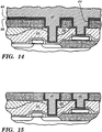
- the remaining steps are analogous to those described in FIGS. 7-9 of the previous embodiment.
- a second layer 44 of titanium/titanium nitride is conformally deposited to coat the surface of the ARC and the trench structure.
- Tungsten 46 is deposited to completely fill the trench and extend over the Ti/TiN and the tungsten is CMP planarized to provide the structure shown in FIG. 15.
Landscapes
- Internal Circuitry In Semiconductor Integrated Circuit Devices (AREA)
- Exposure Of Semiconductors, Excluding Electron Or Ion Beam Exposure (AREA)
- Formation Of Insulating Films (AREA)
Applications Claiming Priority (2)
| Application Number | Priority Date | Filing Date | Title |
|---|---|---|---|
| US29040294A | 1994-08-15 | 1994-08-15 | |
| US290402 | 2002-11-08 |
Publications (2)
| Publication Number | Publication Date |
|---|---|
| EP0697723A2 true EP0697723A2 (fr) | 1996-02-21 |
| EP0697723A3 EP0697723A3 (fr) | 1997-04-16 |
Family
ID=23115842
Family Applications (1)
| Application Number | Title | Priority Date | Filing Date |
|---|---|---|---|
| EP95480097A Withdrawn EP0697723A3 (fr) | 1994-08-15 | 1995-07-24 | Procédé de métallisation d'une couche isolante |
Country Status (3)
| Country | Link |
|---|---|
| US (1) | US5882999A (fr) |
| EP (1) | EP0697723A3 (fr) |
| JP (1) | JPH08191047A (fr) |
Cited By (3)
| Publication number | Priority date | Publication date | Assignee | Title |
|---|---|---|---|---|
| GB2332774A (en) * | 1997-12-24 | 1999-06-30 | Plessey Semiconductors Ltd | Method of forming contacts to semiconductor device regions |
| EP0959496A3 (fr) * | 1998-05-22 | 1999-12-15 | Applied Materials, Inc. | Procédé pour la fabrication d'une couche diélectrique auto-planarisée pour une rainure d'isolation |
| WO2000010202A1 (fr) * | 1998-08-12 | 2000-02-24 | Applied Materials, Inc. | Ligne d'interconnexion formee par double damasquinage utilisant des couches dielectriques ayant des caracteristiques d'attaque dissemblables |
Families Citing this family (23)
| Publication number | Priority date | Publication date | Assignee | Title |
|---|---|---|---|---|
| KR100230392B1 (ko) * | 1996-12-05 | 1999-11-15 | 윤종용 | 반도체 소자의 콘택 플러그 형성방법 |
| US6107190A (en) * | 1997-01-30 | 2000-08-22 | Nec Corporation | Method of fabricating semiconductor device |
| US6060385A (en) * | 1997-02-14 | 2000-05-09 | Micro Technology, Inc. | Method of making an interconnect structure |
| US6372630B1 (en) * | 1997-04-18 | 2002-04-16 | Nippon Steel Corporation | Semiconductor device and fabrication method thereof |
| US6930028B1 (en) * | 1997-06-09 | 2005-08-16 | Texas Instruments Incorporated | Antireflective structure and method |
| US6020258A (en) * | 1997-07-07 | 2000-02-01 | Yew; Tri-Rung | Method for unlanded via etching using etch stop |
| KR100278652B1 (ko) * | 1998-01-13 | 2001-02-01 | 윤종용 | 반도체장치의텅스텐패턴형성방법 |
| US6004850A (en) * | 1998-02-23 | 1999-12-21 | Motorola Inc. | Tantalum oxide anti-reflective coating (ARC) integrated with a metallic transistor gate electrode and method of formation |
| US6121098A (en) * | 1998-06-30 | 2000-09-19 | Infineon Technologies North America Corporation | Semiconductor manufacturing method |
| US6090674A (en) * | 1998-11-09 | 2000-07-18 | Taiwan Semiconductor Manufacturing Company | Method of forming a hole in the sub quarter micron range |
| US7071101B1 (en) * | 1998-12-09 | 2006-07-04 | Advanced Micro Devices, Inc. | Sacrificial TiN arc layer for increased pad etch throughput |
| US6140224A (en) * | 1999-04-19 | 2000-10-31 | Worldiwide Semiconductor Manufacturing Corporation | Method of forming a tungsten plug |
| US6162722A (en) * | 1999-05-17 | 2000-12-19 | United Microelectronics Corp. | Unlanded via process |
| US6410443B1 (en) * | 1999-08-27 | 2002-06-25 | Advanced Micro Devices, Inc. | Method for removing semiconductor ARC using ARC CMP buffing |
| DE19948568A1 (de) * | 1999-10-08 | 2001-04-19 | Infineon Technologies Ag | Ätzverfahren für Dual-Damascene Anwendungen |
| KR100363642B1 (ko) * | 1999-11-11 | 2002-12-05 | 아남반도체 주식회사 | 반도체 소자의 접촉부 형성 방법 |
| US6444557B1 (en) | 2000-03-14 | 2002-09-03 | International Business Machines Corporation | Method of forming a damascene structure using a sacrificial conductive layer |
| JP2002289592A (ja) * | 2001-03-28 | 2002-10-04 | Sony Corp | 半導体装置の製造方法 |
| US6866943B2 (en) | 2002-04-30 | 2005-03-15 | Infineon Technologies Ag | Bond pad structure comprising tungsten or tungsten compound layer on top of metallization level |
| KR20040057079A (ko) * | 2002-12-24 | 2004-07-02 | 동부전자 주식회사 | 반도체 소자의 커패시터 및 콘택홀 동시 제조 방법 |
| US20050221612A1 (en) * | 2004-04-05 | 2005-10-06 | International Business Machines Corporation | A low thermal budget (mol) liner, a semiconductor device comprising said liner and method of forming said semiconductor device |
| US7422981B2 (en) * | 2005-12-07 | 2008-09-09 | Canon Kabushiki Kaisha | Method for manufacturing semiconductor device by using dual damascene process and method for manufacturing article having communicating hole |
| US8883021B2 (en) * | 2012-03-30 | 2014-11-11 | Taiwan Semiconductor Manufacturing Company, Ltd. | MEMS nanostructures and methods of forming the same |
Citations (2)
| Publication number | Priority date | Publication date | Assignee | Title |
|---|---|---|---|---|
| US4783248A (en) | 1987-02-10 | 1988-11-08 | Siemens Aktiengesellschaft | Method for the production of a titanium/titanium nitride double layer |
| US4920073A (en) | 1989-05-11 | 1990-04-24 | Texas Instruments, Incorporated | Selective silicidation process using a titanium nitride protective layer |
Family Cites Families (16)
| Publication number | Priority date | Publication date | Assignee | Title |
|---|---|---|---|---|
| US4657628A (en) * | 1985-05-01 | 1987-04-14 | Texas Instruments Incorporated | Process for patterning local interconnects |
| US4770479A (en) * | 1985-07-01 | 1988-09-13 | Raytheon Company | Optical elements having buried layers and method of manufacture |
| US4789648A (en) * | 1985-10-28 | 1988-12-06 | International Business Machines Corporation | Method for producing coplanar multi-level metal/insulator films on a substrate and for forming patterned conductive lines simultaneously with stud vias |
| IT1197776B (it) * | 1986-07-15 | 1988-12-06 | Gte Telecom Spa | Processo per l'ottenimento di circuiti passivi a strato sottile con linee resistive a differenti resistenze di strato e circuito passivo realizzato con il processo suddetto |
| US4826785A (en) * | 1987-01-27 | 1989-05-02 | Inmos Corporation | Metallic fuse with optically absorptive layer |
| US4884123A (en) * | 1987-02-19 | 1989-11-28 | Advanced Micro Devices, Inc. | Contact plug and interconnect employing a barrier lining and a backfilled conductor material |
| US5173442A (en) * | 1990-07-23 | 1992-12-22 | Microelectronics And Computer Technology Corporation | Methods of forming channels and vias in insulating layers |
| US5225372A (en) * | 1990-12-24 | 1993-07-06 | Motorola, Inc. | Method of making a semiconductor device having an improved metallization structure |
| DE69225082T2 (de) * | 1991-02-12 | 1998-08-20 | Matsushita Electronics Corp | Halbleiter-Vorrichtung mit Verdrahtung der verbesserten Zuverlässigkeit und Verfahren zu ihner Herstellung |
| US5219788A (en) * | 1991-02-25 | 1993-06-15 | Ibm Corporation | Bilayer metallization cap for photolithography |
| EP0525942A2 (fr) * | 1991-05-31 | 1993-02-03 | AT&T Corp. | Procédé de fabrication d'un circuit intégré utilisant deux couches de matériau de réserve |
| US5124780A (en) * | 1991-06-10 | 1992-06-23 | Micron Technology, Inc. | Conductive contact plug and a method of forming a conductive contact plug in an integrated circuit using laser planarization |
| TW520072U (en) * | 1991-07-08 | 2003-02-01 | Samsung Electronics Co Ltd | A semiconductor device having a multi-layer metal contact |
| JPH0547936A (ja) * | 1991-08-20 | 1993-02-26 | Fujitsu Ltd | 半導体装置の製造方法 |
| JPH0685075A (ja) * | 1992-07-17 | 1994-03-25 | Yamaha Corp | 多層配線形成法 |
| US5403781A (en) * | 1992-07-17 | 1995-04-04 | Yamaha Corporation | Method of forming multilayered wiring |
-
1995
- 1995-07-24 EP EP95480097A patent/EP0697723A3/fr not_active Withdrawn
- 1995-08-09 JP JP7203115A patent/JPH08191047A/ja active Pending
-
1996
- 1996-08-05 US US08/692,319 patent/US5882999A/en not_active Expired - Fee Related
Patent Citations (2)
| Publication number | Priority date | Publication date | Assignee | Title |
|---|---|---|---|---|
| US4783248A (en) | 1987-02-10 | 1988-11-08 | Siemens Aktiengesellschaft | Method for the production of a titanium/titanium nitride double layer |
| US4920073A (en) | 1989-05-11 | 1990-04-24 | Texas Instruments, Incorporated | Selective silicidation process using a titanium nitride protective layer |
Cited By (4)
| Publication number | Priority date | Publication date | Assignee | Title |
|---|---|---|---|---|
| GB2332774A (en) * | 1997-12-24 | 1999-06-30 | Plessey Semiconductors Ltd | Method of forming contacts to semiconductor device regions |
| GB2332774B (en) * | 1997-12-24 | 2002-10-30 | Plessey Semiconductors Ltd | Insulated gate bipolar transistor |
| EP0959496A3 (fr) * | 1998-05-22 | 1999-12-15 | Applied Materials, Inc. | Procédé pour la fabrication d'une couche diélectrique auto-planarisée pour une rainure d'isolation |
| WO2000010202A1 (fr) * | 1998-08-12 | 2000-02-24 | Applied Materials, Inc. | Ligne d'interconnexion formee par double damasquinage utilisant des couches dielectriques ayant des caracteristiques d'attaque dissemblables |
Also Published As
| Publication number | Publication date |
|---|---|
| EP0697723A3 (fr) | 1997-04-16 |
| US5882999A (en) | 1999-03-16 |
| JPH08191047A (ja) | 1996-07-23 |
Similar Documents
| Publication | Publication Date | Title |
|---|---|---|
| US5882999A (en) | Process for metallization of an insulation layer | |
| US6424039B2 (en) | Dual damascene process using sacrificial spin-on materials | |
| US6420257B2 (en) | Process for forming trenches and contacts during the formation of a semiconductor memory device | |
| US6066569A (en) | Dual damascene process for metal layers and organic intermetal layers | |
| US6458705B1 (en) | Method for forming via-first dual damascene interconnect structure | |
| US5670298A (en) | Method of forming a metal pattern in manufacturing a semiconductor device | |
| US4657629A (en) | Bilevel resist process | |
| US5893748A (en) | Method for producing semiconductor devices with small contacts, vias, or damascene trenches | |
| US6326278B1 (en) | Method of protecting an alignment mark when manufacturing a semiconductor device | |
| US5057186A (en) | Method of taper-etching with photoresist adhesion layer | |
| KR100443064B1 (ko) | 집적 회로내의 소규모 구조 형성을 위한 이미지 리버설 방법 | |
| US6465157B1 (en) | Dual layer pattern formation method for dual damascene interconnect | |
| EP0188735B1 (fr) | Procédé pour ajuster la pente des parois d'un trou de contact dans une couche isolante | |
| WO1999054930A1 (fr) | Metallisation profonde submicromique a l'aide de photoresist pour ultraviolets lointains | |
| US5422312A (en) | Method for forming metal via | |
| JPH07307333A (ja) | パターン形成方法 | |
| US7241684B2 (en) | Method of forming metal wiring of semiconductor device | |
| KR100384876B1 (ko) | 반도체소자에서의 개선된 듀얼 대머신 공정 | |
| US6451706B1 (en) | Attenuation of reflecting lights by surface treatment | |
| EP0554123A1 (fr) | Procédé de fabrication d'un contact | |
| KR0124638B1 (ko) | 반도체장치의 다층배선 형성방법 | |
| US5958797A (en) | Planarization of a patterned structure on a substrate using an ion implantation-assisted wet chemical etch | |
| US6281092B1 (en) | Method for manufacturing a metal-to-metal capacitor utilizing only one masking step | |
| KR0168358B1 (ko) | 반도체 장치의 미세 접촉창 형성 방법 | |
| KR0124633B1 (ko) | 아이엠디(imd)를 이용한 메탈패턴 형성방법 |
Legal Events
| Date | Code | Title | Description |
|---|---|---|---|
| PUAI | Public reference made under article 153(3) epc to a published international application that has entered the european phase |
Free format text: ORIGINAL CODE: 0009012 |
|
| AK | Designated contracting states |
Kind code of ref document: A2 Designated state(s): DE FR GB |
|
| 17P | Request for examination filed |
Effective date: 19960626 |
|
| PUAL | Search report despatched |
Free format text: ORIGINAL CODE: 0009013 |
|
| AK | Designated contracting states |
Kind code of ref document: A3 Designated state(s): DE FR GB |
|
| STAA | Information on the status of an ep patent application or granted ep patent |
Free format text: STATUS: THE APPLICATION HAS BEEN WITHDRAWN |
|
| 18W | Application withdrawn |
Withdrawal date: 19970528 |
|
| RIN1 | Information on inventor provided before grant (corrected) |
Inventor name: KERSZKOWSKI, GLORIA JEAN Inventor name: ANDERSON, CHRISTINE ANN Inventor name: BUKER, EDWARD DANIEL Inventor name: THOMAS, DAVID CHARLES Inventor name: CRONIN, JOHN EDWARD |