EP0697733A2 - Dispositif de protection contre les décharges électrostatiques et procédé de fabrication associé - Google Patents
Dispositif de protection contre les décharges électrostatiques et procédé de fabrication associé Download PDFInfo
- Publication number
- EP0697733A2 EP0697733A2 EP95111588A EP95111588A EP0697733A2 EP 0697733 A2 EP0697733 A2 EP 0697733A2 EP 95111588 A EP95111588 A EP 95111588A EP 95111588 A EP95111588 A EP 95111588A EP 0697733 A2 EP0697733 A2 EP 0697733A2
- Authority
- EP
- European Patent Office
- Prior art keywords
- conductivity type
- dopant region
- dopant
- region
- forming
- Prior art date
- Legal status (The legal status is an assumption and is not a legal conclusion. Google has not performed a legal analysis and makes no representation as to the accuracy of the status listed.)
- Withdrawn
Links
- 238000000034 method Methods 0.000 title claims abstract description 32
- 239000002019 doping agent Substances 0.000 claims abstract description 107
- 239000004065 semiconductor Substances 0.000 claims abstract description 24
- 239000000758 substrate Substances 0.000 claims abstract description 23
- 125000006850 spacer group Chemical group 0.000 claims abstract description 10
- 230000003071 parasitic effect Effects 0.000 abstract description 5
- 239000000463 material Substances 0.000 description 10
- 229920002120 photoresistant polymer Polymers 0.000 description 10
- 239000003989 dielectric material Substances 0.000 description 8
- 239000012535 impurity Substances 0.000 description 8
- 230000015556 catabolic process Effects 0.000 description 3
- 239000004020 conductor Substances 0.000 description 3
- 238000012545 processing Methods 0.000 description 3
- VYPSYNLAJGMNEJ-UHFFFAOYSA-N Silicium dioxide Chemical compound O=[Si]=O VYPSYNLAJGMNEJ-UHFFFAOYSA-N 0.000 description 2
- 229910052782 aluminium Inorganic materials 0.000 description 2
- XAGFODPZIPBFFR-UHFFFAOYSA-N aluminium Chemical compound [Al] XAGFODPZIPBFFR-UHFFFAOYSA-N 0.000 description 2
- 230000015572 biosynthetic process Effects 0.000 description 2
- 239000011248 coating agent Substances 0.000 description 2
- 238000000576 coating method Methods 0.000 description 2
- 230000003247 decreasing effect Effects 0.000 description 2
- 238000004519 manufacturing process Methods 0.000 description 2
- 238000012986 modification Methods 0.000 description 2
- 230000004048 modification Effects 0.000 description 2
- 238000012360 testing method Methods 0.000 description 2
- ZOXJGFHDIHLPTG-UHFFFAOYSA-N Boron Chemical compound [B] ZOXJGFHDIHLPTG-UHFFFAOYSA-N 0.000 description 1
- ZOKXTWBITQBERF-UHFFFAOYSA-N Molybdenum Chemical compound [Mo] ZOKXTWBITQBERF-UHFFFAOYSA-N 0.000 description 1
- 229910052581 Si3N4 Inorganic materials 0.000 description 1
- XUIMIQQOPSSXEZ-UHFFFAOYSA-N Silicon Chemical compound [Si] XUIMIQQOPSSXEZ-UHFFFAOYSA-N 0.000 description 1
- RTAQQCXQSZGOHL-UHFFFAOYSA-N Titanium Chemical compound [Ti] RTAQQCXQSZGOHL-UHFFFAOYSA-N 0.000 description 1
- 238000013459 approach Methods 0.000 description 1
- 229910052796 boron Inorganic materials 0.000 description 1
- 230000007423 decrease Effects 0.000 description 1
- 238000009792 diffusion process Methods 0.000 description 1
- 229910052751 metal Inorganic materials 0.000 description 1
- 239000002184 metal Substances 0.000 description 1
- 229910052750 molybdenum Inorganic materials 0.000 description 1
- 239000011733 molybdenum Substances 0.000 description 1
- 230000003647 oxidation Effects 0.000 description 1
- 238000007254 oxidation reaction Methods 0.000 description 1
- 230000021715 photosynthesis, light harvesting Effects 0.000 description 1
- 229910021420 polycrystalline silicon Inorganic materials 0.000 description 1
- 229920005591 polysilicon Polymers 0.000 description 1
- 229910052710 silicon Inorganic materials 0.000 description 1
- 239000010703 silicon Substances 0.000 description 1
- 235000012239 silicon dioxide Nutrition 0.000 description 1
- 239000000377 silicon dioxide Substances 0.000 description 1
- HQVNEWCFYHHQES-UHFFFAOYSA-N silicon nitride Chemical compound N12[Si]34N5[Si]62N3[Si]51N64 HQVNEWCFYHHQES-UHFFFAOYSA-N 0.000 description 1
- 229910052715 tantalum Inorganic materials 0.000 description 1
- GUVRBAGPIYLISA-UHFFFAOYSA-N tantalum atom Chemical compound [Ta] GUVRBAGPIYLISA-UHFFFAOYSA-N 0.000 description 1
- 229910052719 titanium Inorganic materials 0.000 description 1
- 239000010936 titanium Substances 0.000 description 1
- WFKWXMTUELFFGS-UHFFFAOYSA-N tungsten Chemical compound [W] WFKWXMTUELFFGS-UHFFFAOYSA-N 0.000 description 1
- 229910052721 tungsten Inorganic materials 0.000 description 1
- 239000010937 tungsten Substances 0.000 description 1
Images


Classifications
-
- H—ELECTRICITY
- H10—SEMICONDUCTOR DEVICES; ELECTRIC SOLID-STATE DEVICES NOT OTHERWISE PROVIDED FOR
- H10D—INORGANIC ELECTRIC SEMICONDUCTOR DEVICES
- H10D89/00—Aspects of integrated devices not covered by groups H10D84/00 - H10D88/00
- H10D89/60—Integrated devices comprising arrangements for electrical or thermal protection, e.g. protection circuits against electrostatic discharge [ESD]
- H10D89/601—Integrated devices comprising arrangements for electrical or thermal protection, e.g. protection circuits against electrostatic discharge [ESD] for devices having insulated gate electrodes, e.g. for IGFETs or IGBTs
- H10D89/611—Integrated devices comprising arrangements for electrical or thermal protection, e.g. protection circuits against electrostatic discharge [ESD] for devices having insulated gate electrodes, e.g. for IGFETs or IGBTs using diodes as protective elements
-
- H—ELECTRICITY
- H10—SEMICONDUCTOR DEVICES; ELECTRIC SOLID-STATE DEVICES NOT OTHERWISE PROVIDED FOR
- H10D—INORGANIC ELECTRIC SEMICONDUCTOR DEVICES
- H10D8/00—Diodes
- H10D8/411—PN diodes having planar bodies
Definitions
- the present invention relates, in general, to electrical protection devices, and more particularly, to integrated devices which protect monolithic integrated circuits from damage by large voltage transients.
- monolithic integrated circuits may become damaged by exposing their input or output terminals to large and sudden voltage transients such as electrostatic discharges.
- electrostatic charge may build up on personnel and test equipment.
- the built-up electrostatic charge discharges and may force large currents into the integrated devices.
- the large currents may rupture dielectric materials within the integrated devices such as gate oxides or it may melt conductive materials such as polysilicon or aluminum interconnects, thereby irreparably damaging the integrated circuits.
- protection devices that shunt current away from input and output circuitry within the integrated devices, thereby preventing damage to the integrated devices by large voltage transients.
- One technique for protecting integrated device input and output circuitry is to form current shunting structures from parasitic elements present in the integrated devices. A disadvantage of this technique is that the breakdown voltages of these structures is limited by the processing techniques of the particular integrated circuit.
- Another technique for protecting these circuits is to improve the energy dissipation capability of the protection circuitry. This is done by laying out the protection circuit to have larger geometries, wider metal interconnects, more and larger contacts, increased spacing, etc.
- SCR silicon controlled rectifiers
- the present invention provides an electrostatic discharge (ESD) protection device and a method for fabricating the device.
- the electrostatic discharge protection device is fabricated in a region of a semiconductor substrate that is free of a field oxide. This region is referred to as an active region for the electrostatic discharge protection device.
- the electrostatic discharge protection device is a diode comprising an N-region spaced apart from a P-region.
- the N and P regions are fabricated by coating the semiconductor substrate with a layer of photoresist, forming openings in the layer of photoresist to expose portions of the semiconductor substrate, and implanting or diffusing an impurity material of N conductivity type into one of the exposed portions of the semiconductor substrate to form the N-region, and implanting or diffusing an impurity material of P conductivity type into another of the exposed portions of the semiconductor substrate to form the P-region. Then, electrodes are formed to contact the N-region and the P-region.
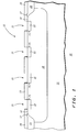
- FIG. 1 illustrates a highly enlarged cross-sectional view of a portion 10 of an ESD protection device during processing in accordance with an embodiment of the present invention.
- a semiconductor substrate 11 of N conductivity type having a major surface 12 and an active region 13 surrounded by a field oxide 14.
- the portions of field oxide 14 adjacent major surface 12 are shown as having a bulges or bumps 17.
- bulges 17 result from an oxidation step during the formation of field oxide 14 and are commonly referred to as a bird's heads. Techniques for forming field oxide 14 and the resulting bird's heads 17 are well known to those skilled in the art.
- active region 13 includes a dopant region or dopant well 18 of P conductivity type extending vertically from major surface 12 into semiconductor substrate 11 and extending laterally under portions of field oxide 14.
- Dopant region 18, also referred to as a well or tub, may be formed by implanting a dopant or impurity material of P conductivity type such as, for example, boron into active region 13.
- dopant region 18 may be formed by diffusing the P type impurity material into active region 13.
- dopant region 18 has a junction depth ranging between approximately 3 microns ( ⁇ m) and approximately 5 ⁇ m and a surface concentration of P type impurity material in dopant region 18 ranges between approximately 1 x 10¹⁶ atoms per cubic centimeter (atoms/cm3) and approximately 1 x 10¹⁹ atoms/cm3.
- Techniques for forming dopant region 18 are well known to those skilled in the art. It should be understood that the conductivity type of semiconductor substrate 11 and dopant region 18 is not a limitation of the present invention. In other words, semiconductor substrate 11 may be of P conductivity type and dopant region 18 may be of N conductivity type. It should be further understood that the formation of dopant region 18 is optional.
- Major surface 12 and field oxide 14 are coated with a layer of photoresist 19. Then, openings 21 are formed in layer of photoresist 19 to expose portions of major surface 12. Techniques for coating major surface 12 and field oxide 14 with layer of photoresist 19 and forming openings 21 in layer of photoresist 19 are well known to those skilled in the art.
- An impurity material of P conductivity type is implanted through openings 21 into semiconductor substrate 11 to form dopant regions 22 having sidewalls 25. More particularly, the impurity material is implanted into dopant region 18.
- dopant regions 22 have a junction depth ranging between approximately 0.2 ⁇ m and approximately 0.4 ⁇ m and a surface concentration ranging between approximately 1.0 x 10¹⁵ atoms/cm3 and approximately 1.0 x 10¹⁶ atoms/cm3.
- layer of photoresist 19 is removed from major surface 12 and field oxide 14 using techniques well known to those skilled in the art.
- FIG. 2 major surface 12 and field oxide 14 are coated with a layer of photoresist 23. It should be understood that the same reference numerals are used in the figures to denote the same elements. Then, openings 24 are formed in layer of photoresist 23 to expose portions of major surface 12. An impurity material of N conductivity type is implanted through openings 24 into semiconductor substrate 11 to form dopant regions 27 having sidewalls 28, wherein sidewalls 28 form metallurgical junctions with dopant region 18.
- dopant regions 27 have a junction depth ranging between approximately 0.1 ⁇ m and approximately 0.25 ⁇ m and a surface concentration ranging between approximately 1 x 10¹⁶ atoms/cm3 and approximately 6 x 10²⁰ atoms/cm3, and a distance between adjacent sidewalls 25 and 28 of the first dopant region and the second dopant region, respectively, is at least 1 micron. It should be noted that each dopant region 27 is between two adjacent dopant regions 22 and that at least one of the dopant regions 27 is adjacent to one of the two adjacent dopant regions 22. Moreover, it should be noted that regions 27 and regions 22 can be interchanged.
- dopant regions 27 are interdigitated with and spaced apart from dopant regions 22.
- layer of photoresist 23 is removed.
- dopant regions 22 and 27 may be formed using diffusion techniques. It should be understood that the shape, junction depths and surface concentrations provided for the examples of regions 22 and 27 are not limitations of the present invention.
- interdigitated dopant regions 22 and 27 forms plurality of parallel diode structures, wherein the spacer regions 29 between adjacent sidewalls 25 and 28 set the series resistance of each diode structure.
- the series resistance of each diode may be decreased by decreasing the distance between sidewalls 25 and 28 of adjacent dopant regions 22 and 27, respectively, and increased by increasing the distance between these sidewalls 25 and 28.
- field oxide is not formed in active region 13 and in particular in spacer regions 29, i.e., between sidewalls 25 and 28 of adjacent dopant regions 22 and 27, respectively.
- sidewalls 25 and 28 serve as active diode regions, thereby increasing the active diode area for a specified chip area.
- layer of dielectric material 31 includes silicon dioxide, nitride, and the like.
- layer of dielectric material 31 has a thickness ranging between approximately 5,000 angstroms and approximately 7,000 angstroms.
- openings 32 are formed in layer of dielectric material 31 to expose a portion of surface 12 of dopant regions 22 and 27.
- Anode electrodes 33 are formed by filling openings 32 exposing surface 12 of dopant regions 22 with a conductive material.
- Cathode electrodes 34 are formed by filling openings 34 exposing surface 12 of dopant regions 27 with a conductive material.
- anode electrodes 33 contact dopant regions 22 and cathode electrodes 34 contact dopant regions 27.
- Suitable materials for electrodes 33 and 34 include aluminum, titanium, tungsten, molybdenum, tantalum, and combinations thereof. Techniques for forming electrodes in contact with dopant regions are known to those skilled in the art.
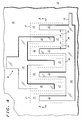
- FIG. 4 a top view of the portion 10 of the ESD protection device of FIG. 3 is illustrated.
- the location of dopant regions 22 and 27 below layer of dielectric material 31 are illustrated by broken lines 37 and 38, respectively.
- the spacer regions 29 are indicated by arrows 39.
- Anode electrodes 33 are shown as a plurality of conductive fingers over dopant regions 22 and portions of layer of dielectric material 31.
- anode electrodes 33 are coupled to a ground potential via extension 41.
- Cathode electrodes 34 are shown as a plurality of conductive fingers over dopant regions 27 and portions of layer of dielectric material 31.
- portions of cathode electrodes 34 are interdigitated with portions of anode electrodes 33 and a portion of cathode 34 is coupled to contact pad 42.
- Electrostatic discharge protection devices manufactured in accordance with the present invention may have dopant regions in an area less than 2,000 square microns, wherein a machine model ESD voltage of the electrostatic discharge protection device is at least 500 volts.
- the ESD protection device of the present invention is fabricated in an active region that is devoid of field oxide.
- the ESD protection device is a diode comprising two dopant regions that are spaced apart from each other, wherein the spacer region between the two dopant regions is devoid of field oxide.
- the absence of field oxide in the spacer region lowers the parasitic diode resistance between the two dopant regions and permits the depletion regions formed at the junctions of regions 27 and 18 to spread freely under reverse bias conditions. If the depletion zone spreads all the way across the spacer regions, the diode will exhibit a reduced breakdown voltage. The reduced parasitic resistance and the reduced breakdown voltage both result in reduced energy passed into the integrated circuit being protected. Since the locations of the dopant regions are photolithographically defined, the width of the spacer regions, i.e., the distance between the two dopant regions, is limited by the resolution of the photolithographic technique rather than by the width of the field oxide between said dopant regions. Further, the active area of the protection device includes the sidewalls of the dopant regions, resulting in a larger active area of the protection device. In addition, the junction that breaks down for the protection device of the present invention is the junction between dopant regions 18 and 27.
Landscapes
- Semiconductor Integrated Circuits (AREA)
- Metal-Oxide And Bipolar Metal-Oxide Semiconductor Integrated Circuits (AREA)
- Insulated Gate Type Field-Effect Transistor (AREA)
Applications Claiming Priority (2)
| Application Number | Priority Date | Filing Date | Title |
|---|---|---|---|
| US283437 | 1988-12-12 | ||
| US08/283,437 US5597758A (en) | 1994-08-01 | 1994-08-01 | Method for forming an electrostatic discharge protection device |
Publications (2)
| Publication Number | Publication Date |
|---|---|
| EP0697733A2 true EP0697733A2 (fr) | 1996-02-21 |
| EP0697733A3 EP0697733A3 (fr) | 1996-11-06 |
Family
ID=23086066
Family Applications (1)
| Application Number | Title | Priority Date | Filing Date |
|---|---|---|---|
| EP95111588A Withdrawn EP0697733A3 (fr) | 1994-08-01 | 1995-07-24 | Dispositif de protection contre les décharges électrostatiques et procédé de fabrication associé |
Country Status (5)
| Country | Link |
|---|---|
| US (1) | US5597758A (fr) |
| EP (1) | EP0697733A3 (fr) |
| JP (1) | JPH0864772A (fr) |
| KR (1) | KR960009180A (fr) |
| CN (1) | CN1122519A (fr) |
Cited By (2)
| Publication number | Priority date | Publication date | Assignee | Title |
|---|---|---|---|---|
| WO2004061913A3 (fr) * | 2002-12-31 | 2004-08-26 | Intel Corp | Diodes de protection contre les decharges electrostatiques de faible capacite |
| CN104576763A (zh) * | 2014-12-31 | 2015-04-29 | 杭州士兰集成电路有限公司 | 一种二极管结构及其制造方法 |
Families Citing this family (24)
| Publication number | Priority date | Publication date | Assignee | Title |
|---|---|---|---|---|
| US6211001B1 (en) * | 1998-07-24 | 2001-04-03 | Sharp Laboratories Of America, Inc. | Electrostatic discharge protection for salicided devices and method of making same |
| JP4025023B2 (ja) * | 2001-01-18 | 2007-12-19 | 株式会社東芝 | 半導体装置 |
| US6878581B1 (en) * | 2001-02-22 | 2005-04-12 | United Microelectronics Corp. | Electrostatic discharge protection structure and a method for forming the same |
| CN100401512C (zh) * | 2002-03-26 | 2008-07-09 | 华邦电子股份有限公司 | 利用硅控整流器的静电放电保护电路 |
| DE10238798B3 (de) * | 2002-08-23 | 2004-03-18 | Infineon Technologies Ag | Hochfrequenzschalter |
| US7132696B2 (en) * | 2002-08-28 | 2006-11-07 | Micron Technology, Inc. | Intermeshed guard bands for multiple voltage supply structures on an integrated circuit, and methods of making same |
| US6888248B2 (en) * | 2003-03-26 | 2005-05-03 | Taiwan Semiconductor Manufacturing Co., Ltd | Extended length metal line for improved ESD performance |
| JP2004296998A (ja) * | 2003-03-28 | 2004-10-21 | Matsushita Electric Ind Co Ltd | 半導体装置 |
| JP4759982B2 (ja) * | 2003-12-18 | 2011-08-31 | 株式会社デンソー | ダイオード |
| CN1316618C (zh) * | 2004-03-31 | 2007-05-16 | 矽统科技股份有限公司 | 半导体装置、静电放电防护装置及其制造方法 |
| JP4495512B2 (ja) * | 2004-05-11 | 2010-07-07 | パナソニック株式会社 | 固体撮像装置 |
| US7189610B2 (en) * | 2004-10-18 | 2007-03-13 | Semiconductor Components Industries, L.L.C. | Semiconductor diode and method therefor |
| KR100781487B1 (ko) * | 2006-07-18 | 2007-12-03 | 문학범 | 높은 써지 내량 과 빠른 반응 속도를 갖는 과전압 보호 칩 |
| US7764316B2 (en) * | 2007-03-15 | 2010-07-27 | Fairchild Imaging, Inc. | CCD array with integrated high voltage protection circuit |
| KR101431759B1 (ko) * | 2008-04-30 | 2014-08-20 | 삼성전자주식회사 | 정전기적 방전 보호용 다이오드 |
| EP2400546A1 (fr) * | 2010-06-22 | 2011-12-28 | Oticon A/S | Protection ESD dans un procédé BI-CMOS ou CMOS standard qui accepte des entrées/sorties à haute tension |
| JP2013058640A (ja) * | 2011-09-08 | 2013-03-28 | Toshiba Corp | 半導体装置 |
| US8766365B2 (en) * | 2012-02-21 | 2014-07-01 | Micron Technology, Inc. | Circuit-protection devices |
| KR102011174B1 (ko) * | 2012-09-27 | 2019-08-14 | 로무 가부시키가이샤 | 칩 다이오드 및 그 제조 방법 |
| US9728529B2 (en) * | 2014-04-14 | 2017-08-08 | Infineon Technologies Dresden Gmbh | Semiconductor device with electrostatic discharge protection structure |
| US10734330B2 (en) * | 2015-01-30 | 2020-08-04 | Taiwan Semiconductor Manufacturing Company Limited | Semiconductor devices having an electro-static discharge protection structure |
| CN106653747A (zh) * | 2016-12-29 | 2017-05-10 | 北京宇翔电子有限公司 | 一种防esd的二极管及包含其的cmos集成电路保护电路 |
| US10163893B1 (en) | 2017-08-28 | 2018-12-25 | Micron Technologies, Inc. | Apparatus containing circuit-protection devices |
| US10431577B2 (en) | 2017-12-29 | 2019-10-01 | Micron Technology, Inc. | Methods of forming circuit-protection devices |
Family Cites Families (12)
| Publication number | Priority date | Publication date | Assignee | Title |
|---|---|---|---|---|
| US3396317A (en) * | 1965-11-30 | 1968-08-06 | Texas Instruments Inc | Surface-oriented high frequency diode |
| JPS5365078A (en) * | 1976-11-24 | 1978-06-10 | Toshiba Corp | Production of junction type field effect transistor |
| US4189739A (en) * | 1978-03-08 | 1980-02-19 | Bell Telephone Laboratories, Incorporated | Semiconductor overload protection structure |
| US4322882A (en) * | 1980-02-04 | 1982-04-06 | Fairchild Camera & Instrument Corp. | Method for making an integrated injection logic structure including a self-aligned base contact |
| US4596605A (en) * | 1982-12-14 | 1986-06-24 | Junichi Nishizawa | Fabrication process of static induction transistor and solid-state image sensor device |
| US5060037A (en) * | 1987-04-03 | 1991-10-22 | Texas Instruments Incorporated | Output buffer with enhanced electrostatic discharge protection |
| US4736271A (en) * | 1987-06-23 | 1988-04-05 | Signetics Corporation | Protection device utilizing one or more subsurface diodes and associated method of manufacture |
| JP2513010B2 (ja) * | 1988-12-27 | 1996-07-03 | 日本電気株式会社 | 半導体集積回路の入力保護装置 |
| EP0401410B1 (fr) * | 1989-06-08 | 1993-12-29 | Siemens Aktiengesellschaft | Circuit de protection de circuits électroniques contre les surtensions |
| JPH07114210B2 (ja) * | 1990-01-26 | 1995-12-06 | 株式会社東芝 | 半導体装置の製造方法 |
| US5138413A (en) * | 1990-10-22 | 1992-08-11 | Harris Corporation | Piso electrostatic discharge protection device |
| EP0519741B1 (fr) * | 1991-06-21 | 1997-05-02 | Kabushiki Kaisha Toshiba | Elément semi-conducteur à haute tension de claquage |
-
1994
- 1994-08-01 US US08/283,437 patent/US5597758A/en not_active Expired - Lifetime
-
1995
- 1995-07-24 EP EP95111588A patent/EP0697733A3/fr not_active Withdrawn
- 1995-07-25 JP JP7208566A patent/JPH0864772A/ja active Pending
- 1995-07-31 CN CN95109683A patent/CN1122519A/zh active Pending
- 1995-08-01 KR KR1019950023619A patent/KR960009180A/ko not_active Ceased
Non-Patent Citations (1)
| Title |
|---|
| None |
Cited By (4)
| Publication number | Priority date | Publication date | Assignee | Title |
|---|---|---|---|---|
| WO2004061913A3 (fr) * | 2002-12-31 | 2004-08-26 | Intel Corp | Diodes de protection contre les decharges electrostatiques de faible capacite |
| US7847317B2 (en) | 2002-12-31 | 2010-12-07 | Intel Corporation | Low-capacitance electrostatic discharge protection diodes |
| US8304807B2 (en) | 2002-12-31 | 2012-11-06 | Intel Corporation | Low-capacitance electrostatic discharge protection diodes |
| CN104576763A (zh) * | 2014-12-31 | 2015-04-29 | 杭州士兰集成电路有限公司 | 一种二极管结构及其制造方法 |
Also Published As
| Publication number | Publication date |
|---|---|
| KR960009180A (ko) | 1996-03-22 |
| CN1122519A (zh) | 1996-05-15 |
| US5597758A (en) | 1997-01-28 |
| JPH0864772A (ja) | 1996-03-08 |
| EP0697733A3 (fr) | 1996-11-06 |
Similar Documents
| Publication | Publication Date | Title |
|---|---|---|
| US5597758A (en) | Method for forming an electrostatic discharge protection device | |
| TWI376078B (en) | Circuit configurations to reduce snapback of a transient voltage suppressor | |
| EP0745275B1 (fr) | Dispositif a diode con u pour proteger les condensateurs metal-oxyde-metal | |
| US6441437B1 (en) | Integrated semiconductor circuit with protective structure for protection against electrostatic discharge | |
| US5856214A (en) | Method of fabricating a low voltage zener-triggered SCR for ESD protection in integrated circuits | |
| US8455315B2 (en) | Symmetric blocking transient voltage suppressor (TVS) using bipolar transistor base snatch | |
| US7327541B1 (en) | Operation of dual-directional electrostatic discharge protection device | |
| US10672758B2 (en) | Electrostatic discharge protection structure, method for manufacturing an electrostatic discharge protection structure, and vertical thyristor structure | |
| US6392266B1 (en) | Transient suppressing device and method | |
| US6320232B1 (en) | Integrated semiconductor circuit with protective structure for protection against electrostatic discharge | |
| JP2004510333A5 (fr) | ||
| JP2004510333A (ja) | 高電圧ダイオードおよびその製造方法 | |
| EP0253105A1 (fr) | Circuit intégré comprenant un dispositif de protection | |
| JPH09293881A (ja) | 静電気放電保護回路の製造方法 | |
| US20040021998A1 (en) | Electrostatic discharge protection device comprising several thyristors | |
| EP0822596A2 (fr) | Circuit de protection ESD | |
| US6061218A (en) | Overvoltage protection device and method for increasing shunt current | |
| KR910000229B1 (ko) | 보호장치를 구비하고 있는 반도체집적회로와 그 제조방법 | |
| US5831312A (en) | Electrostic discharge protection device comprising a plurality of trenches | |
| JP5023254B2 (ja) | 集積回路の静電荷放電保護 | |
| US20020020874A1 (en) | Device for protecting an SOI structure | |
| EP1715527A2 (fr) | Dispositif de protection contre les décharges électrostatiques | |
| EP4340025B1 (fr) | Redresseurs commandés au silicium avec une région flottante segmentée | |
| US7075156B1 (en) | Collector structure for electrostatic discharge protection circuits | |
| US12408366B2 (en) | Protection device structures with a discontinuous isolation well |
Legal Events
| Date | Code | Title | Description |
|---|---|---|---|
| PUAI | Public reference made under article 153(3) epc to a published international application that has entered the european phase |
Free format text: ORIGINAL CODE: 0009012 |
|
| AK | Designated contracting states |
Kind code of ref document: A2 Designated state(s): DE FR GB |
|
| PUAL | Search report despatched |
Free format text: ORIGINAL CODE: 0009013 |
|
| AK | Designated contracting states |
Kind code of ref document: A3 Designated state(s): DE FR GB |
|
| 17P | Request for examination filed |
Effective date: 19970506 |
|
| 17Q | First examination report despatched |
Effective date: 19980626 |
|
| STAA | Information on the status of an ep patent application or granted ep patent |
Free format text: STATUS: THE APPLICATION IS DEEMED TO BE WITHDRAWN |
|
| 18D | Application deemed to be withdrawn |
Effective date: 19981107 |