EP0697757A1 - Circuit de protection contre les décharges électrostatiques pour dispositif de circuit intégré - Google Patents
Circuit de protection contre les décharges électrostatiques pour dispositif de circuit intégré Download PDFInfo
- Publication number
- EP0697757A1 EP0697757A1 EP94630054A EP94630054A EP0697757A1 EP 0697757 A1 EP0697757 A1 EP 0697757A1 EP 94630054 A EP94630054 A EP 94630054A EP 94630054 A EP94630054 A EP 94630054A EP 0697757 A1 EP0697757 A1 EP 0697757A1
- Authority
- EP
- European Patent Office
- Prior art keywords
- circuit
- terminal
- control signal
- integrated circuit
- node
- Prior art date
- Legal status (The legal status is an assumption and is not a legal conclusion. Google has not performed a legal analysis and makes no representation as to the accuracy of the status listed.)
- Withdrawn
Links
- 230000008878 coupling Effects 0.000 claims abstract description 12
- 238000010168 coupling process Methods 0.000 claims abstract description 12
- 238000005859 coupling reaction Methods 0.000 claims abstract description 12
- 230000015556 catabolic process Effects 0.000 claims description 9
- 239000004065 semiconductor Substances 0.000 claims description 7
- 230000005669 field effect Effects 0.000 claims description 4
- 230000004044 response Effects 0.000 claims description 2
- 239000003990 capacitor Substances 0.000 abstract description 16
- 230000003068 static effect Effects 0.000 description 5
- 238000000034 method Methods 0.000 description 4
- 230000007246 mechanism Effects 0.000 description 3
- 229910021420 polycrystalline silicon Inorganic materials 0.000 description 3
- 229920005591 polysilicon Polymers 0.000 description 3
- VYPSYNLAJGMNEJ-UHFFFAOYSA-N Silicium dioxide Chemical compound O=[Si]=O VYPSYNLAJGMNEJ-UHFFFAOYSA-N 0.000 description 2
- 230000006870 function Effects 0.000 description 2
- 238000006731 degradation reaction Methods 0.000 description 1
- 230000001419 dependent effect Effects 0.000 description 1
- 238000010586 diagram Methods 0.000 description 1
- 230000003292 diminished effect Effects 0.000 description 1
- 230000005611 electricity Effects 0.000 description 1
- 238000004519 manufacturing process Methods 0.000 description 1
- 229910044991 metal oxide Inorganic materials 0.000 description 1
- 150000004706 metal oxides Chemical class 0.000 description 1
- 235000012239 silicon dioxide Nutrition 0.000 description 1
- 239000000377 silicon dioxide Substances 0.000 description 1
Images

Classifications
-
- H—ELECTRICITY
- H02—GENERATION; CONVERSION OR DISTRIBUTION OF ELECTRIC POWER
- H02H—EMERGENCY PROTECTIVE CIRCUIT ARRANGEMENTS
- H02H9/00—Emergency protective circuit arrangements for limiting excess current or voltage without disconnection
- H02H9/04—Emergency protective circuit arrangements for limiting excess current or voltage without disconnection responsive to excess voltage
- H02H9/045—Emergency protective circuit arrangements for limiting excess current or voltage without disconnection responsive to excess voltage adapted to a particular application and not provided for elsewhere
- H02H9/046—Emergency protective circuit arrangements for limiting excess current or voltage without disconnection responsive to excess voltage adapted to a particular application and not provided for elsewhere responsive to excess voltage appearing at terminals of integrated circuits
Definitions
- the present invention relates, in general, to an electrostatic discharge (“ESD”) protection circuit for an integrated circuit (“IC”) device. More particularly, the present invention relates to a readily implemented ESD protection circuit for an integrated circuit device which utilizes a single transistor coupled between relatively high capacitance circuit nodes, such as the external V CC and V SS pins.
- ESD electrostatic discharge
- MOSFETs metal oxide semiconductor field effect transistors
- capacitors utilizing a thin gate oxide or shallow junctions are especially susceptible to damage from ESD, even bipolar circuits may be damaged by sufficiently high static discharges resulting in altered electrical properties and diminished reliability.
- one method which is currently employed to provide ESD protection is to incorporate an input protection network or other output protection circuit comprising a number of diodes coupled to the device input/output ("I/O") pins integrated monolithically with the integrated circuit.
- the function of such diodes is to provide a breakdown mechanism lower than that of any other circuit elements to which they are electrically connected.
- breakdown mechanisms have become increasingly more difficult to implement as thinner gate oxides and shallower junctions are utilized in constructing integrated circuits and this technique inevitably leads to poor ESD protection on the V CC input pin or results in other circuit design compromises in order to increase the breakdown resistance to ESD.
- the protection of circuitry coupled to the V CC and V SS pins is especially problematic due to the fact that they are coupled to virtually all of the IC's internal circuitry.
- the present invention relates to a readily implemented integrated ESD protection circuit of especial utility with respect to the high capacitance nodes of an integrated circuit, and in particular, the V CC and V SS or other IC voltage input pins.
- the ESD protection circuit of the present invention incorporates a single transistor or switching device coupling, for example, the integrated circuit V CC and V SS input pins.
- a capacitor coupled between the V CC input pin and the control terminal of the transistor causes the transistor to turn “on” thereby limiting the V CC voltage by shunting it to V SS .
- a resistor coupled between the V SS input pin and the transistor control terminal causes the gate of the transistor to be pulled to ground thereby turning the transistor "off".
- the values for the capacitor and resistor are chosen such that the resultant time constant is long relative to a Human Body Model ESD test circuit and short relative to typical voltage rise times encountered at the protected circuit nodes. As a result, the ESD current is discharged through the transistor before the resistor can turn it "off” and the transistor is held in that state during normal operation and throughout normal fluctuations in supply voltage.
- an integrated circuit device including first and second input terminals thereof, the integrated circuit including an electrostatic discharge protection circuit.
- the electrostatic discharge protection circuit includes a switching device having first, second and control terminals thereof with the first and second terminals being coupled respectively to the first and second input terminals of the integrated circuit device.
- a capacitive element couples the first and control terminals of the switching device and a resistive element couples the second and control terminals of the switching device.
- an electrostatic discharge protection circuit for an integrated circuit which includes first and second external terminals thereof.
- the electrostatic protection circuit includes a field effect transistor having source, drain and gate terminals thereof with the source terminal being coupled to the first external terminal and the drain terminal being coupled to the second external terminal.
- a capacitor couples the gate terminal to the source terminal and a resistor couples the gate terminal to the drain terminal.
- an integrated circuit device including at least first and second circuit nodes thereof with the integrated circuit device including an electrostatic discharge protection circuit.
- the electrostatic discharge protection circuit includes a switchable shunting means having a first state thereof for operatively coupling the first circuit node to the second circuit node in response to a control signal supplied to a control terminal of the shunting means.
- the switchable shunting means also includes a second state thereof for operatively isolating the first circuit node from the second circuit node in an absence of the control signal.
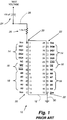
- the integrated circuit 12 comprises a conventional integrated circuit memory device incorporating a number of input/output (“I/O") pins 14 designated, for example, as data input/output pins DQ1-DQ8.
- Integrated circuit 12 also incorporates a number of control input pins 16 corresponding to active low: write enable ("/WE”), row address select (“/RAS”), column address select (“/CAS”) and output enable (“/OE").
- integrated circuit 12 also includes a number of input pins 18 shown as corresponding to the address pins, or terminals A0-A9, for coupling to an address bus utilized in accessing particular locations within the memory array of the integrated circuit 12.
- a number of voltage input pins for supplying power to integrated circuit 12 are indicated as V CC and V SS pins 20,22 respectively and more than one of each may be provided to help ensure low noise/high speed operation.
- the voltage applied to V CC pin 20 may correspond to a power level of approximately +5 volts while the V SS pin 22 will be connected to circuit ground 30 as shown.
- a 100 picoFarad (“pF") capacitor 24 is charged to a test voltage and then discharged into a test pin of the integrated circuit 12, for example the V CC pin 20, through a 1.5Kohm resistor 26 as shown by means of a test line 28 connected thereto.
- pF picoFarad
- an input protection network 31 is shown for utilization in conjunction with I/O pins 14 and/or input pins 18 of the exemplary integrated circuit 12 shown in Fig. 1.
- Input protection network 31 is integrated as part of the semiconductor die comprising the integrated circuit elements of integrated circuit 12 and is coupled to an input pin 32 as shown.
- Input protection network 31 may typically comprise a pair of resistors 34,36 in conjunction with diodes 38,40.
- diode 38 has its cathode coupled to the V CC pin of the integrated circuit 12 and its anode coupled to the cathode of diode 40 forming a node 35.
- diode 40 has its anode connected to the V SS pin of the integrated circuit 12.
- Resistor 34 couples node 35 to input pin 32 while resistor 36 couples node 35 to the related input circuitry of the integrated circuit 12.
- a conventional output protection circuit 41 for the output pins of an integrated circuit 12 as shown in Fig. 1 is illustrated.
- the output protection circuit 41 comprises a pair of diodes 46,48 having a common node therebetween connected to output pin 42.
- Output pin 42 is also coupled to the output circuitry of a typical integrated circuit 12 as shown in Fig. 1.
- Diode 46 has its cathode coupled to the V CC pin of the integrated circuit and its anode coupled to the cathode of diode 48 which in turn has its anode coupled to the V SS pin.
- Over voltage protection circuit 50 typically comprises a number of series connected zener diodes herein designated as 52a, 52b through 52n.
- the zener diodes 52 are coupled in series such that the cathode of the first zener diode 52a is connected to the V CC pin 20 and the anode of the last of the series of zener diodes 52n is coupled to the V SS pin 22.
- the V CC pin 20 is connected to many circuit elements on the integrated circuit die and some, or many, of these elements may breakdown before the over voltage protection circuit 50 can provide the desired protection. Should this occur, the circuit elements integrated on the integrated circuit 12 die may be damaged as they are not designed to carry the relatively large currents which result from an applied ESD. With respect to the various protection schemes illustrated in Figs. 2A through 2C, protection against ESD is dependent upon breakdown mechanisms which are required to be lower than that of the other circuit elements of the integrated circuit itself. Such techniques lead to inherently poor ESD protection on the V CC pin 20 or other circuit design compromises necessary to increase breakdown voltage.
- ESD protection circuit 60 in accordance with the present invention is shown.
- ESD protection circuit 60 may be monolithically integrated with the other circuit elements of an integrated circuit 61, the outline of which is shown in phantom.
- ESD protection circuit 60 comprises, in pertinent part, a transistor 62, (shown, for example, as an n-channel MOSFET), which functions as a switching or shunting device between terminal, (or node), 64 coupled to V CC and terminal, (or node), 66 coupled to V SS .
- transistor 62 may comprise a device having a channel width of 2,000 microns and a channel length of 1.2 microns.
- the gate of transistor 62 is coupled to a node 68 as shown.
- ESD protection circuit 60 also comprises a capacitor 70 coupling terminal 64 to node 68.
- capacitor 70 may be a conventional integrated circuit polysilicon/silicon dioxide/polysilicon capacitor having a desired capacitance of approximately 25pF.
- ESD protection circuit 60 further comprises a resistor 72 coupling terminal 66 to node 68.
- resistor 72 may be a conventional integrated circuit polysilicon element having a preferred resistance of approximately 20Kohms.
- capacitor 70 couples the gate of transistor 62 at node 68 "high", thereby causing transistor 62 to turn “on”. This, in turn, serves to limit the V CC voltage by shunting it to V SS .
- the resistor 72 then causes the gate of the transistor 62 at node 68 to be pulled to circuit ground at pin V SS thereby turning the transistor 62 "off” after the ESD current is discharged through the transistor 62.
- the values of capacitor 70, resistor 72 and the conductance of transistor 62 should be chosen such that the RC time constant of the capacitor 70 and resistor 72 is larger than the RC time constant of the 100 picoFarad capacitor 24 and 1.5Kohm resistor 26 of the test configuration 10 illustrated in Fig. 1. Moreover, the RC time constant of the capacitor 70 and resistor 72 of the ESD protection circuit 60 must be short compared to the rise times of V CC in actual system applications wherein the supply voltage fluctuations occur over hundreds of microseconds.
- the conductance of transistor 62 is chosen such that it is high enough to keep V CC below the breakdown voltage of any circuits located on the integrated circuit die.
Landscapes
- Engineering & Computer Science (AREA)
- Microelectronics & Electronic Packaging (AREA)
- Semiconductor Integrated Circuits (AREA)
- Emergency Protection Circuit Devices (AREA)
- Protection Of Static Devices (AREA)
- Elimination Of Static Electricity (AREA)
- Logic Circuits (AREA)
Applications Claiming Priority (2)
| Application Number | Priority Date | Filing Date | Title |
|---|---|---|---|
| US29113294A | 1994-08-16 | 1994-08-16 | |
| US291132 | 1994-08-16 |
Publications (1)
| Publication Number | Publication Date |
|---|---|
| EP0697757A1 true EP0697757A1 (fr) | 1996-02-21 |
Family
ID=23118996
Family Applications (1)
| Application Number | Title | Priority Date | Filing Date |
|---|---|---|---|
| EP94630054A Withdrawn EP0697757A1 (fr) | 1994-08-16 | 1994-09-15 | Circuit de protection contre les décharges électrostatiques pour dispositif de circuit intégré |
Country Status (2)
| Country | Link |
|---|---|
| EP (1) | EP0697757A1 (fr) |
| JP (1) | JPH08275375A (fr) |
Cited By (6)
| Publication number | Priority date | Publication date | Assignee | Title |
|---|---|---|---|---|
| WO2003081742A1 (fr) * | 2002-03-22 | 2003-10-02 | Freescale Semiconductor, Inc. | Circuit de protection contre les decharges electrostatiques |
| WO2006040211A1 (fr) * | 2004-10-16 | 2006-04-20 | Robert Bosch Gmbh | Circuit integre relevant de la technologie dite 'smart power' |
| US7209332B2 (en) | 2002-12-10 | 2007-04-24 | Freescale Semiconductor, Inc. | Transient detection circuit |
| US7634396B2 (en) | 2002-04-25 | 2009-12-15 | Freescale Semiconductor, Inc. | Method and computer program product for generation of bus functional models |
| US8970239B2 (en) | 2010-09-27 | 2015-03-03 | International Business Machines Corporation | Methods and systems for detecting ESD events in cabled devices |
| EP3035785A1 (fr) | 2014-12-18 | 2016-06-22 | Endress + Hauser GmbH + Co. KG | Dispositif et procede d'implantation automatisee d'au moins un composant electronique dans une plaquette |
Families Citing this family (2)
| Publication number | Priority date | Publication date | Assignee | Title |
|---|---|---|---|---|
| JP4516102B2 (ja) | 2007-09-26 | 2010-08-04 | 株式会社東芝 | Esd保護回路 |
| CN102089949B (zh) * | 2008-07-11 | 2016-08-03 | 小威廉·R·本纳 | 用于光电子器件的故障保护器及相关方法 |
Citations (3)
| Publication number | Priority date | Publication date | Assignee | Title |
|---|---|---|---|---|
| JPS592358A (ja) * | 1982-06-28 | 1984-01-07 | Mitsubishi Electric Corp | 半導体回路の保護回路 |
| EP0435047A2 (fr) * | 1989-12-19 | 1991-07-03 | National Semiconductor Corporation | Protection contre des décharges électrostatiques pour circuits intégrés |
| JPH03289164A (ja) * | 1990-04-05 | 1991-12-19 | Matsushita Electron Corp | 保護回路および保護装置 |
-
1994
- 1994-09-15 EP EP94630054A patent/EP0697757A1/fr not_active Withdrawn
-
1995
- 1995-06-20 JP JP7175606A patent/JPH08275375A/ja active Pending
Patent Citations (3)
| Publication number | Priority date | Publication date | Assignee | Title |
|---|---|---|---|---|
| JPS592358A (ja) * | 1982-06-28 | 1984-01-07 | Mitsubishi Electric Corp | 半導体回路の保護回路 |
| EP0435047A2 (fr) * | 1989-12-19 | 1991-07-03 | National Semiconductor Corporation | Protection contre des décharges électrostatiques pour circuits intégrés |
| JPH03289164A (ja) * | 1990-04-05 | 1991-12-19 | Matsushita Electron Corp | 保護回路および保護装置 |
Non-Patent Citations (2)
| Title |
|---|
| PATENT ABSTRACTS OF JAPAN vol. 16, no. 120 (E - 1182) 26 March 1992 (1992-03-26) * |
| PATENT ABSTRACTS OF JAPAN vol. 8, no. 81 (E - 238)<1518> 13 April 1984 (1984-04-13) * |
Cited By (9)
| Publication number | Priority date | Publication date | Assignee | Title |
|---|---|---|---|---|
| WO2003081742A1 (fr) * | 2002-03-22 | 2003-10-02 | Freescale Semiconductor, Inc. | Circuit de protection contre les decharges electrostatiques |
| US7154719B2 (en) | 2002-03-22 | 2006-12-26 | Freescale Semiconductor, Inc. | Circuit for electrostatic discharge protection |
| US7634396B2 (en) | 2002-04-25 | 2009-12-15 | Freescale Semiconductor, Inc. | Method and computer program product for generation of bus functional models |
| US7209332B2 (en) | 2002-12-10 | 2007-04-24 | Freescale Semiconductor, Inc. | Transient detection circuit |
| WO2006040211A1 (fr) * | 2004-10-16 | 2006-04-20 | Robert Bosch Gmbh | Circuit integre relevant de la technologie dite 'smart power' |
| US8970239B2 (en) | 2010-09-27 | 2015-03-03 | International Business Machines Corporation | Methods and systems for detecting ESD events in cabled devices |
| US10249330B2 (en) | 2010-09-27 | 2019-04-02 | International Business Machines Corporation | Methods and systems for detecting ESD events in cabled devices |
| EP3035785A1 (fr) | 2014-12-18 | 2016-06-22 | Endress + Hauser GmbH + Co. KG | Dispositif et procede d'implantation automatisee d'au moins un composant electronique dans une plaquette |
| DE102014119077A1 (de) | 2014-12-18 | 2016-06-23 | Endress + Hauser Gmbh + Co. Kg | Vorrichtung und Verfahren zum automatisierten Bestücken einer Leiterplatte mit zumindest einem elektronischen Bauteil |
Also Published As
| Publication number | Publication date |
|---|---|
| JPH08275375A (ja) | 1996-10-18 |
Similar Documents
| Publication | Publication Date | Title |
|---|---|---|
| US6385021B1 (en) | Electrostatic discharge (ESD) protection circuit | |
| US6430016B1 (en) | Setpoint silicon controlled rectifier (SCR) electrostatic discharge (ESD) core clamp | |
| US5276582A (en) | ESD protection using npn bipolar transistor | |
| JPH07321628A (ja) | ヒステリシストリガ回路を用いる静電放電保護 | |
| US5917689A (en) | General purpose EOS/ESD protection circuit for bipolar-CMOS and CMOS integrated circuits | |
| KR19980024304A (ko) | 집적회로를 위한 비파괴 트리거형 정전기 방전 보호회로 및 그 방법 | |
| US11114848B2 (en) | ESD protection charge pump active clamp for low-leakage applications | |
| US7589945B2 (en) | Distributed electrostatic discharge protection circuit with varying clamp size | |
| US10978444B2 (en) | RC-triggered bracing circuit | |
| US20210013714A1 (en) | Electrostatic discharge protection circuit and operation method | |
| JP7632076B2 (ja) | Esd保護回路、半導体装置、電子機器 | |
| US11876366B2 (en) | Overvoltage protection | |
| US5821797A (en) | Protection circuit for semiconductor devices | |
| US20020017690A1 (en) | Semiconductor integrated circuit | |
| US5654863A (en) | Integrated circuit having a gate oxide | |
| US10749336B2 (en) | ESD protection circuit with passive trigger voltage controlled shut-off | |
| US5990723A (en) | Filter circuits for protecting against transient electrical pulses | |
| EP0802604A2 (fr) | Circuit de protection | |
| JPH08275375A (ja) | 静電放電保護回路およびこれを備えた集積回路装置 | |
| EP1482554B1 (fr) | Dispositif de protection contre les décharges électrostatiques | |
| US9142953B2 (en) | Electrostatic discharge protection apparatus and associated method | |
| US5903184A (en) | Semiconductor device having protection circuit | |
| US11811221B2 (en) | Electrostatic discharge protection device | |
| JP3025373B2 (ja) | 半導体集積回路 | |
| CN114204535B (zh) | 一种具有加速关断的阻断型浪涌保护器 |
Legal Events
| Date | Code | Title | Description |
|---|---|---|---|
| PUAI | Public reference made under article 153(3) epc to a published international application that has entered the european phase |
Free format text: ORIGINAL CODE: 0009012 |
|
| AK | Designated contracting states |
Kind code of ref document: A1 Designated state(s): DE FR GB IT NL |
|
| STAA | Information on the status of an ep patent application or granted ep patent |
Free format text: STATUS: THE APPLICATION IS DEEMED TO BE WITHDRAWN |
|
| 18D | Application deemed to be withdrawn |
Effective date: 19960822 |
|
| ITF | It: translation for a ep patent filed |