EP0697790A2 - Procédé et circuit d'insertion d'image dans l'image - Google Patents
Procédé et circuit d'insertion d'image dans l'image Download PDFInfo
- Publication number
- EP0697790A2 EP0697790A2 EP95111018A EP95111018A EP0697790A2 EP 0697790 A2 EP0697790 A2 EP 0697790A2 EP 95111018 A EP95111018 A EP 95111018A EP 95111018 A EP95111018 A EP 95111018A EP 0697790 A2 EP0697790 A2 EP 0697790A2
- Authority
- EP
- European Patent Office
- Prior art keywords
- line
- image
- faded
- field
- picture
- Prior art date
- Legal status (The legal status is an assumption and is not a legal conclusion. Google has not performed a legal analysis and makes no representation as to the accuracy of the status listed.)
- Granted
Links
- 238000000034 method Methods 0.000 title claims abstract description 37
- 238000003780 insertion Methods 0.000 title description 2
- 230000037431 insertion Effects 0.000 title description 2
- 230000015654 memory Effects 0.000 claims abstract description 58
- 238000012937 correction Methods 0.000 claims abstract description 32
- 238000011156 evaluation Methods 0.000 claims abstract 3
- 230000008569 process Effects 0.000 claims description 8
- 238000006243 chemical reaction Methods 0.000 claims description 7
- 238000005562 fading Methods 0.000 claims description 5
- 230000003111 delayed effect Effects 0.000 claims description 4
- 230000006978 adaptation Effects 0.000 claims description 3
- 238000001514 detection method Methods 0.000 claims description 3
- 230000006870 function Effects 0.000 claims description 2
- 230000033001 locomotion Effects 0.000 description 4
- 230000000750 progressive effect Effects 0.000 description 4
- 230000008859 change Effects 0.000 description 3
- 230000006872 improvement Effects 0.000 description 3
- 230000006735 deficit Effects 0.000 description 2
- 238000010586 diagram Methods 0.000 description 2
- 230000009467 reduction Effects 0.000 description 2
- 230000008030 elimination Effects 0.000 description 1
- 238000003379 elimination reaction Methods 0.000 description 1
- 230000001360 synchronised effect Effects 0.000 description 1
Images

Classifications
-
- H—ELECTRICITY
- H04—ELECTRIC COMMUNICATION TECHNIQUE
- H04N—PICTORIAL COMMUNICATION, e.g. TELEVISION
- H04N5/00—Details of television systems
- H04N5/44—Receiver circuitry for the reception of television signals according to analogue transmission standards
- H04N5/445—Receiver circuitry for the reception of television signals according to analogue transmission standards for displaying additional information
- H04N5/45—Picture in picture, e.g. displaying simultaneously another television channel in a region of the screen
Definitions
- the invention relates to a method for picture-in-picture insertion of an image to be inserted into a main picture.
- the invention also relates to a circuit arrangement for performing the method.
- Such a method can be used in devices for video signal processing, e.g. B. televisions are used in which flicker relief of the images to be displayed on the screen is achieved by doubling the playback line frequency.
- a process for picture-in-picture fade-in is carried out by the integrated circuit SDA 9088 from Siemens.
- the image to be faded in is temporarily stored in a memory which has only the storage capacity of one field. With any phase position of the main picture and the picture to be faded in, reading out at twice the line frequency may result in the reading process overtaking the writing process in the field memory.
- parts of the picture from two successive movement phases are then displayed.
- the line on which the jump in motion is visible is called the jointline.
- the interlaced first and second fields of the picture to be faded in the television set only every second field is buffered in the field memory of the specified integrated circuit. Then only fields of the same line grid position are available for overlay. Grid swaps when a jointline occurs are avoided. However, the vertical resolution of the image to be faded in is relatively low.
- European patent application EP 0 471 878 shows a method and a circuit arrangement for carrying out the method for picture-in-picture fade-in, in which two field memories are used for the picture to be faded in. Fields of only one line grid position are stored in each of the field memories. A decision device ensures that the output side is switched between the field memories in such a way that a jointline-free display is made possible. A raster correction device ensures that the entire joint-free field to be faded in is displayed in the main image with the correct grid. The interpolation to be carried out on the complete fields for raster correction leads to a reduction in the vertical resolution. Another disadvantage is the relatively high circuit complexity due to the use of two field memories.
- European patent application EP-A-0 229 431 describes a method for picture-in-picture fading in which a field memory is used for only one field. Reading from the field memory is carried out at a simple line frequency. Measures for correcting line scrambling are carried out in order to enable low-interference reproduction. The corrective measures provide for a change in the readout counter by +/- 1 line depending on the relative position of the write to read counters of the field memory for the image to be inserted and the line grid position of the main image and the image to be inserted. An application for a picture-in-picture overlay with a doubled display line frequency is not described.
- the object of the invention is to provide a method for picture-in-picture overlay according to the type mentioned at the beginning with a doubled display line frequency, in which a Memory is required for only one field of the image to be faded in and this enables fade-in as flawlessly as possible.
- Another task is to specify a circuit arrangement for performing the method.
- a circuit arrangement for performing the method is specified in claim 8.
- the line-by-line adaptation of the picture content of the picture to be faded in to the line grid position of the main picture prevents grid swaps when a joint line is present. Since both fields are used for fading in, the vertical resolution is considerably increased.
- the method according to the invention can be applied to various conventional flicker reduction methods for the main image. This applies both to upconversion processes with field doubling with inter-field or intra-field processing and to progressive conversion processes.
- the correction signal can be implemented by a logic device, by means of which the field association of the line to be faded in and the grid position of the point at which it is to be faded in in the main image are evaluated.
- a switchover between direct reading out of the memory a delay by one line or an interpolation from, for example, two successive ones can be carried out Lines.
- the circuitry complexity is consequently relatively low.
- the effort for address control of the field memory can be reduced or a saving of storage effort for a picture line can be achieved by a field line to be faded in, which is assigned to a field for a first ( ⁇ ) line screen position, in the large picture in the second line screen position ( ⁇ ) and vice versa is shown.
- a field line to be faded in which is assigned to a field for a first ( ⁇ ) line screen position, in the large picture in the second line screen position ( ⁇ ) and vice versa is shown.
- the first field In order to ensure the correct interlacing of the first and second fields in the displayed image, the first field must be shifted down one line compared to the second field.
- the smallest data unit that can be addressed in the memory can be a field line, part of a field line (for example a line half or a line third, etc.) or even a pixel.
- the correction signal for controlling the raster adaptation of the image to be superimposed on the main image is then expediently updated synchronously with the reading out of a new line, a new line portion or a new image point.
- switching between the different regulations for grid adjustment with the change of the correction signal may also be carried out within a line to be faded in.
- the line index diagram according to FIG. 1 shows an example of the selected phase position between the main image and the image to be faded in.
- Timeline 1 shows the grid position sequence for the main picture.
- the playback grid ⁇ is available.
- the playback grid runs at twice the line frequency, z. B. 100Hz.
- the timeline 2 is related to the fields of the image to be faded in, which are read in there in the sequence B0, A1, B1, ...
- the write and read addresses of the field memory are plotted along the vertical axis.
- the pointer 10 corresponds to the reading of the image B0 into the field memory. It is assumed that the field memory has already been written with field A0.
- interlaced fields are received, ie the field sequence A0, B0, A1, B1, ...
- the fields A0, A1 comprise the odd-numbered lines of a frame, the fields B0, B1 the even-numbered lines.
- the grid ⁇ also contains the even-numbered lines, the grid ⁇ the odd-numbered lines.
- the single line frequency e.g. B. 50Hz
- read fields of the image to be faded in are read out at twice the line frequency.
- Each readout process is represented by a pointer 13 ... 18.
- the readout from the field memory is synchronized with the line frame of the main picture. Because reading the lines from the field memory occurs faster than the reading in, the reading and reading pointers overlap.
- read-in and read-out pointers can form two intersection points 19, 20. This means that, for example, for read-out addresses of the read-out pointer 15 below the intersection point 19 with the read-in pointer 11, image lines of the field A1 just written are read out; for readout addresses above the intersection 19, the lines belonging to the previously stored field B0 are read out.
- a joint line is determined on the screen in accordance with the intersection point 19, the image information already belonging to the new movement phase of the field A1 being shown in the upper part of the image, and the image information of the previous movement phase of the field B0 is shown below this joint line.
- the field to be read out according to the pointer 15 is to be represented in the ⁇ -raster of the main picture in accordance with the time line 1. Without further control measures, the grid would be swapped when the lines from field A1 belong to field B0, which the viewer would find extremely disruptive.
- the image line to be faded in is corrected such that the image content is adapted to the line grid position of the main image at which the line is to be faded in.
- a correction signal is generated which switches over at the output of the field memory.
- the first fields A are displayed unchanged in the grid ⁇ and the second fields B in the grid ⁇ unchanged. If a field A, B to be faded in is to be displayed in the respective other raster, an interpolation of two lines successively read out from the field memory is carried out.
- lines of a field A are displayed unchanged in raster ⁇ .
- the lines of a field B In order to ensure correct line intermingling with lines of a field B, which is to be represented in the raster ⁇ , the lines of a field B must be shifted down one line compared to the lines of a field A. This is achieved by a delay of one field line when reading out a field B. If lines of a field A to be faded in are to be represented in the grid ⁇ or lines of a field B to be faded in the grid ⁇ , a grid conversion, that is to say an interpolation, must be carried out in each case.
- Table 1 Main image grid Lines of field to be displayed Correction 1st execution Correction 2nd execution ⁇ A - interpolation ⁇ B interpolation delay ⁇ A interpolation - ⁇ B - interpolation
- Table 2 The sequence of the corrections to be carried out between the times 25 and 30 is shown in Table 2 for the phase relationship from the main image to the image to be faded in, as shown in FIG. This period comprises the grid sequence ⁇ 1, ⁇ 2, ⁇ 1, ⁇ 2.
- Table 2 Main image grid field to be displayed Correction 1st execution Correction 2nd execution ⁇ 1 A1 - interpolation B0 interpolation delay ⁇ 2 A1 - interpolation B0 interpolation delay ⁇ 1 B1 - interpolation A1 interpolation - ⁇ 2 B1 - interpolation A1 interpolation -
- the corrections given by way of example in the table can also be applied to corresponding other phase positions from the main image to the image to be faded in.
- the sequence of the corrective measures changes accordingly using Table 1.
- the correction instructions given in Table 1 can also be used if the grid sequence ⁇ is carried out in the main picture.
- the implementation rule in Table 1 also applies to progressive images in which full images are to be displayed on the screen, each of which alternately has lines with an ⁇ or ⁇ grid position.
- the grid correction always ensures that the picture to be faded in is displayed correctly in the main picture, whereby the jointline remains.
- the reproduction grid ⁇ and ⁇ depending on the phase position of the picture to be faded in and the main picture, as shown in FIG. 1, a maximum of two joint lines can alternate.
- a progressive playback grid ⁇ + ⁇ at most one joint line occurs.
- Table 3 Main image grid Memory read area field to be displayed Correction 1st execution Correction 2nd execution ⁇ 1 X A1 - - Y B0 interpolation delay Z.
- a further embodiment of the method with another regulation for generating the correction signal is shown in Table 3 using the example of the phase position of the main image and the image to be faded in, as shown in FIG. 1.
- This embodiment can be used if the same reproduction grid is present at least twice in succession, for example in the reproduction grid ⁇ .
- the various readout areas of the field memory delimited by the joint lines are evaluated for the image to be displayed. As already stated, there are two joint lines 19, 20 for a field to be faded in, which do not occur in the same but in the successive readout cycles 15 and 16, respectively.
- the respective address areas of the field memory delimited by the joint lines are denoted by X, Y, Z.
- an interpolation is to be carried out for the same lines of the field to be faded in, in order to convert the lines belonging to field A1 to the grid position ⁇ .
- an interpolation must be carried out for the same lines of the field to be faded in, in order to convert the corresponding lines belonging to field B0 to the ⁇ raster.
- no interpolations are carried out in the time segments 31, 32 and 33, 34, but the respective lines of fields A1 and B0 are faded in unchanged.
- the lines of field B0 may be delayed by to carry out a line in order to ensure the correct line intermingling with the lines from the fields A0 and A1, which are to be shown before and after in the ⁇ -grid.
- This increases the vertical resolution in these areas 31, 32 and 33, 34.
- one image line is not Display brought so that the image content is shifted by this image line in the vertical direction, but this impairment is hardly noticed by the viewer, so that an overall improvement in quality is achieved by the improved vertical resolution.
- an improvement in the vertical resolution can be achieved for the first and second embodiments in the reproduction rasters ⁇ 1, ⁇ 2 for the readout areas Z and X, respectively.
- the read-out range X or Z is determined, for example, by comparing the readout address with the address at which jointline 19 or 20 is present.
- the respective positions of the joint lines 19, 20 are in turn determined in that the write-in address for the field A1 is overtaken by the read-out addresses for the read-out processes 15, 16.
- the correction rules shown in Table 3 for an exemplary phase position from the main picture to the picture to be faded in can be transferred to other phase positions of the display raster ⁇ by, for those areas in which immediately after one another for two identical display rasters for the same lines of the picture to be faded in instead of an interpolation corresponding to the Tables 1 and 2 an unchanged fade-in is carried out according to Table 3.
- the field memory can be addressed line by line.
- the grid position correction is therefore only carried out line-synchronously.
- Field memories can also be used, which are stored in sections of a line, e.g. B. half line or third line, etc., or pixel by address are addressable.
- the overwriting of image information that has already been saved with newly imported image information to be faded in, that is, the overwriting of the write-in and read-out address, can be within one line.
- the correction signal is within a line with each newly addressed line section or pixel updated. The switchover between the various raster corrections to be carried out then lies within the relevant line.
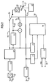
- a video signal for the main picture can be fed in at a connection 51, to which method steps for flicker elimination are applied in a device 70.
- the line frequency is doubled in the device 70.
- the field rate can be doubled or a progressive conversion can be carried out.
- a video signal for the image to be inserted can be applied to a connection 50.
- An analog-digital converter device 52 is used for digital processing of the image signal.
- the fields of the image to be faded in are decimated to the image size to be faded in.
- the decimated images are temporarily stored in a memory 54 for a single field.
- the data read from the field memory 54 are converted in a digital-to-analog converter device 60 in a digital-to-analog converter device 60 in accordance with means to be described below for adapting the raster of the picture to be faded in to the current raster position of the main picture, and faded in in a fade-in device 61 at the intended position of the main picture.
- a fade-in control 62 is used to control the switchover between the main picture and the picture to be faded in.
- the information to be displayed on a screen can be tapped at the output connection 77 of the switch.
- a switch 59 is provided which can be switched between three different connections 56, 57, 58.
- the image line read out from the image memory 54 is at the terminal 56 available immediately and unchanged.
- the connection 57 is connected via a line memory 55 to the output of the field memory 54, so that an image line which can be tapped at the connection 57 is shifted downward, ie delayed, by one line in the image.
- the mean value of a line which has just been read can be tapped with the immediately preceding line delayed by the line memory 55.
- the changeover switch 59 is controlled by the correction device 74, at the output connection 76 of which a correction signal indicating the switch position of the changeover switch 59 is generated.
- the correction rules specified in Tables 2 and 3 are evaluated by the device 74, for example a logic device.
- the device 74 is connected on the input side to the following further devices: a device 71 which specifies the grid position of the line of the main picture which is connected to the connection 75 and which is provided for fading in a line of the picture to be faded in; a device 72 which is connected to the output of the field memory 54 and indicates which field of the image to be superimposed can be assigned to the image line to be superimposed; a device 73 which is provided for realizing the correction rules according to Table 3 and indicates in which of the readout areas X, Y or Z the line just read out from the field memory 54 is located.
- the device 73 is supplied with the current read and write addresses of the field memory 54 on the input side at connections 78, 79. As already explained above in connection with Table 3, the device 73 for area detection essentially compares the read and write addresses.
- connection 58 In order to tap an average of two lines to be faded in at connection 58, line memory 55 must be written during a first line period. During the next line period, the mean value can be formed at connection 58 from this line which has just been buffered and the line which has just been read out. For example, if according to the first Embodiment of the method according to Table 1 with a corresponding phase position of the image to be faded in and the main image, a line belonging to a field B of the image to be faded in to a line belonging to the raster position ⁇ is to be interpolated.
- an interpolated line is only available with the second line of the ⁇ grid (third line of the frame).
- an average value to be interpolated from two lines of field A is only available with the second line of the ⁇ -raster (fourth line of the full image) at the earliest. If ordinary serial addressable image memories are used, this means that there are two image line memories in the field memory 54, the image information of which is not used for image overlay.
Landscapes
- Engineering & Computer Science (AREA)
- Multimedia (AREA)
- Signal Processing (AREA)
- Studio Circuits (AREA)
- Television Systems (AREA)
- Image Processing (AREA)
Applications Claiming Priority (2)
| Application Number | Priority Date | Filing Date | Title |
|---|---|---|---|
| DE4429287A DE4429287A1 (de) | 1994-08-18 | 1994-08-18 | Verfahren und Schaltungsanordnung zur Bild-im-Bild-Einblendung |
| DE4429287 | 1994-08-18 |
Publications (3)
| Publication Number | Publication Date |
|---|---|
| EP0697790A2 true EP0697790A2 (fr) | 1996-02-21 |
| EP0697790A3 EP0697790A3 (fr) | 1996-10-16 |
| EP0697790B1 EP0697790B1 (fr) | 1999-11-10 |
Family
ID=6525983
Family Applications (1)
| Application Number | Title | Priority Date | Filing Date |
|---|---|---|---|
| EP95111018A Expired - Lifetime EP0697790B1 (fr) | 1994-08-18 | 1995-07-13 | Procédé et circuit d'insertion d'image dans l'image |
Country Status (3)
| Country | Link |
|---|---|
| EP (1) | EP0697790B1 (fr) |
| DE (2) | DE4429287A1 (fr) |
| ES (1) | ES2139786T3 (fr) |
Cited By (2)
| Publication number | Priority date | Publication date | Assignee | Title |
|---|---|---|---|---|
| EP0765080A3 (fr) * | 1995-09-19 | 1999-07-28 | Siemens Aktiengesellschaft | Procédé et circuit d'insertion d'image dans l'image |
| US7315332B2 (en) | 2002-05-08 | 2008-01-01 | Nxp B.V. | Video and text display with reduced text flicker |
Families Citing this family (1)
| Publication number | Priority date | Publication date | Assignee | Title |
|---|---|---|---|---|
| DE4445805B4 (de) * | 1994-12-21 | 2004-11-04 | Micronas Munich Gmbh | Schaltungsanordnung zur Teletextverarbeitung und Bild-im-Bildeinblendung |
Citations (2)
| Publication number | Priority date | Publication date | Assignee | Title |
|---|---|---|---|---|
| EP0229431A2 (fr) | 1986-01-03 | 1987-07-22 | Koninklijke Philips Electronics N.V. | Récepteur de télévision couleur à insertion d'image |
| EP0471878A1 (fr) | 1990-08-23 | 1992-02-26 | Siemens Aktiengesellschaft | Procédé de superposition image-dans-image et appareil pour suivre ce procédé |
Family Cites Families (3)
| Publication number | Priority date | Publication date | Assignee | Title |
|---|---|---|---|---|
| US4809069A (en) * | 1988-03-10 | 1989-02-28 | North American Philips Corporation | Multifunction memory for digital television |
| JP2912636B2 (ja) * | 1989-08-04 | 1999-06-28 | 松下電器産業株式会社 | 2画面テレビ |
| JPH03112279A (ja) * | 1989-09-26 | 1991-05-13 | Toshiba Corp | 高品位多画面テレビジョン受像機 |
-
1994
- 1994-08-18 DE DE4429287A patent/DE4429287A1/de not_active Withdrawn
-
1995
- 1995-07-13 DE DE59507213T patent/DE59507213D1/de not_active Expired - Fee Related
- 1995-07-13 EP EP95111018A patent/EP0697790B1/fr not_active Expired - Lifetime
- 1995-07-13 ES ES95111018T patent/ES2139786T3/es not_active Expired - Lifetime
Patent Citations (2)
| Publication number | Priority date | Publication date | Assignee | Title |
|---|---|---|---|---|
| EP0229431A2 (fr) | 1986-01-03 | 1987-07-22 | Koninklijke Philips Electronics N.V. | Récepteur de télévision couleur à insertion d'image |
| EP0471878A1 (fr) | 1990-08-23 | 1992-02-26 | Siemens Aktiengesellschaft | Procédé de superposition image-dans-image et appareil pour suivre ce procédé |
Cited By (2)
| Publication number | Priority date | Publication date | Assignee | Title |
|---|---|---|---|---|
| EP0765080A3 (fr) * | 1995-09-19 | 1999-07-28 | Siemens Aktiengesellschaft | Procédé et circuit d'insertion d'image dans l'image |
| US7315332B2 (en) | 2002-05-08 | 2008-01-01 | Nxp B.V. | Video and text display with reduced text flicker |
Also Published As
| Publication number | Publication date |
|---|---|
| ES2139786T3 (es) | 2000-02-16 |
| DE59507213D1 (de) | 1999-12-16 |
| DE4429287A1 (de) | 1996-02-29 |
| EP0697790B1 (fr) | 1999-11-10 |
| EP0697790A3 (fr) | 1996-10-16 |
Similar Documents
| Publication | Publication Date | Title |
|---|---|---|
| DE3151124C2 (fr) | ||
| DE3619019C2 (de) | Digitale Konvergenzkorrekturvorrichtung | |
| DE69417476T2 (de) | Fernsehgerät fähig zum Vergrössern und Verkleinern des Bildes | |
| DE2824561C2 (fr) | ||
| DE69911562T2 (de) | Videoanzeigevorrichtung und -verfahren mit bidirektionellem abtasten | |
| DE69637276T2 (de) | Bildanzeigegerät | |
| EP0445336B1 (fr) | Méthode et dispositif de réduction du scintillement du bord d'une image de télévision | |
| DE68909470T2 (de) | Bildaufnahmegerät. | |
| DE10212911A1 (de) | Elektroendoskopsystem mit Elektroendoskopen mit verschiedenen Pixelanzahlen | |
| DE69027926T2 (de) | Zentrierung eines einlegebildes in einem bild in bild system | |
| DE3330570A1 (de) | Doppelabtastender zeilensprungfreier fernsehempfaenger | |
| DE19545919B4 (de) | Verfahren zum Erzeugen von Bildsignalen im PAL-Format aus Signalen im NTSC-Format | |
| EP0318760A2 (fr) | Récepteur de télévision avec un dispositif de suppression des perturbations de scintillement | |
| DE4327779C1 (de) | Verfahren und Schaltungsanordnung für ein Fernsehgerät zur Verminderung des Flimmerns | |
| EP1125428B1 (fr) | Circuit permettant de transformer un debit binaire | |
| EP0697790B1 (fr) | Procédé et circuit d'insertion d'image dans l'image | |
| EP0739130B1 (fr) | Procédé et circuit d'insertion d'image dans l'image | |
| EP0239800A2 (fr) | Procédé et arrangement de circuit pour la reproduction sans scintillement d'un signal vidéo | |
| DE69121454T2 (de) | Fernsehsignalumwandler | |
| EP0753972A2 (fr) | Procédé d'interpolation intertrame de signaux de différence de couleur et circuit pour la réalisation du procédé | |
| DE4015020A1 (de) | Schaltungsanordnung zum umsetzen eines fernsehsignals | |
| DE19541870C2 (de) | Schaltungsanordnung zum Überblenden zwischen Bildfolgen | |
| DE19534781C1 (de) | Verfahren und Schaltungsanordnung zur Bild-im-Bild-Einblendung | |
| DE4414173C1 (de) | Verfahren zur Umsetzung einer Bildfolge von Halbbildern mit Zeilensprung auf eine Bildfolge von zeilensprungfreien Bildern und Schaltungsanordnung zur Durchführung des Verfahrens | |
| DE4445805B4 (de) | Schaltungsanordnung zur Teletextverarbeitung und Bild-im-Bildeinblendung |
Legal Events
| Date | Code | Title | Description |
|---|---|---|---|
| PUAI | Public reference made under article 153(3) epc to a published international application that has entered the european phase |
Free format text: ORIGINAL CODE: 0009012 |
|
| AK | Designated contracting states |
Kind code of ref document: A2 Designated state(s): DE ES FR GB IT |
|
| PUAL | Search report despatched |
Free format text: ORIGINAL CODE: 0009013 |
|
| AK | Designated contracting states |
Kind code of ref document: A3 Designated state(s): DE ES FR GB IT |
|
| 17P | Request for examination filed |
Effective date: 19970317 |
|
| 17Q | First examination report despatched |
Effective date: 19981027 |
|
| GRAG | Despatch of communication of intention to grant |
Free format text: ORIGINAL CODE: EPIDOS AGRA |
|
| GRAG | Despatch of communication of intention to grant |
Free format text: ORIGINAL CODE: EPIDOS AGRA |
|
| GRAH | Despatch of communication of intention to grant a patent |
Free format text: ORIGINAL CODE: EPIDOS IGRA |
|
| GRAH | Despatch of communication of intention to grant a patent |
Free format text: ORIGINAL CODE: EPIDOS IGRA |
|
| GRAA | (expected) grant |
Free format text: ORIGINAL CODE: 0009210 |
|
| AK | Designated contracting states |
Kind code of ref document: B1 Designated state(s): DE ES FR GB IT |
|
| REF | Corresponds to: |
Ref document number: 59507213 Country of ref document: DE Date of ref document: 19991216 |
|
| ET | Fr: translation filed | ||
| ITF | It: translation for a ep patent filed | ||
| GBT | Gb: translation of ep patent filed (gb section 77(6)(a)/1977) |
Effective date: 20000119 |
|
| REG | Reference to a national code |
Ref country code: ES Ref legal event code: FG2A Ref document number: 2139786 Country of ref document: ES Kind code of ref document: T3 |
|
| PLBE | No opposition filed within time limit |
Free format text: ORIGINAL CODE: 0009261 |
|
| STAA | Information on the status of an ep patent application or granted ep patent |
Free format text: STATUS: NO OPPOSITION FILED WITHIN TIME LIMIT |
|
| 26N | No opposition filed | ||
| REG | Reference to a national code |
Ref country code: GB Ref legal event code: 732E |
|
| REG | Reference to a national code |
Ref country code: GB Ref legal event code: IF02 |
|
| PGFP | Annual fee paid to national office [announced via postgrant information from national office to epo] |
Ref country code: ES Payment date: 20020807 Year of fee payment: 8 |
|
| PG25 | Lapsed in a contracting state [announced via postgrant information from national office to epo] |
Ref country code: ES Free format text: LAPSE BECAUSE OF NON-PAYMENT OF DUE FEES Effective date: 20030714 |
|
| REG | Reference to a national code |
Ref country code: ES Ref legal event code: FD2A Effective date: 20030714 |
|
| PGFP | Annual fee paid to national office [announced via postgrant information from national office to epo] |
Ref country code: DE Payment date: 20080722 Year of fee payment: 14 |
|
| PGFP | Annual fee paid to national office [announced via postgrant information from national office to epo] |
Ref country code: IT Payment date: 20080726 Year of fee payment: 14 Ref country code: FR Payment date: 20080715 Year of fee payment: 14 |
|
| PGFP | Annual fee paid to national office [announced via postgrant information from national office to epo] |
Ref country code: GB Payment date: 20080722 Year of fee payment: 14 |
|
| GBPC | Gb: european patent ceased through non-payment of renewal fee |
Effective date: 20090713 |
|
| REG | Reference to a national code |
Ref country code: FR Ref legal event code: ST Effective date: 20100331 |
|
| PG25 | Lapsed in a contracting state [announced via postgrant information from national office to epo] |
Ref country code: FR Free format text: LAPSE BECAUSE OF NON-PAYMENT OF DUE FEES Effective date: 20090731 |
|
| PG25 | Lapsed in a contracting state [announced via postgrant information from national office to epo] |
Ref country code: GB Free format text: LAPSE BECAUSE OF NON-PAYMENT OF DUE FEES Effective date: 20090713 |
|
| PG25 | Lapsed in a contracting state [announced via postgrant information from national office to epo] |
Ref country code: DE Free format text: LAPSE BECAUSE OF NON-PAYMENT OF DUE FEES Effective date: 20100202 |
|
| PG25 | Lapsed in a contracting state [announced via postgrant information from national office to epo] |
Ref country code: IT Free format text: LAPSE BECAUSE OF NON-PAYMENT OF DUE FEES Effective date: 20090713 |