EP0698967A2 - Circuit associant au moins deux familles logique différentes - Google Patents
Circuit associant au moins deux familles logique différentes Download PDFInfo
- Publication number
- EP0698967A2 EP0698967A2 EP95113041A EP95113041A EP0698967A2 EP 0698967 A2 EP0698967 A2 EP 0698967A2 EP 95113041 A EP95113041 A EP 95113041A EP 95113041 A EP95113041 A EP 95113041A EP 0698967 A2 EP0698967 A2 EP 0698967A2
- Authority
- EP
- European Patent Office
- Prior art keywords
- circuits
- resistor
- circuit
- circuit arrangement
- coupling resistor
- Prior art date
- Legal status (The legal status is an assumption and is not a legal conclusion. Google has not performed a legal analysis and makes no representation as to the accuracy of the status listed.)
- Withdrawn
Links
- 230000008878 coupling Effects 0.000 claims abstract 7
- 238000010168 coupling process Methods 0.000 claims abstract 7
- 238000005859 coupling reaction Methods 0.000 claims abstract 7
- 230000000295 complement effect Effects 0.000 claims description 3
- 239000003990 capacitor Substances 0.000 description 6
- 230000006978 adaptation Effects 0.000 description 1
- 230000005611 electricity Effects 0.000 description 1
Images

Classifications
-
- H—ELECTRICITY
- H04—ELECTRIC COMMUNICATION TECHNIQUE
- H04L—TRANSMISSION OF DIGITAL INFORMATION, e.g. TELEGRAPHIC COMMUNICATION
- H04L25/00—Baseband systems
- H04L25/02—Details ; arrangements for supplying electrical power along data transmission lines
- H04L25/0264—Arrangements for coupling to transmission lines
- H04L25/0298—Arrangement for terminating transmission lines
-
- H—ELECTRICITY
- H03—ELECTRONIC CIRCUITRY
- H03K—PULSE TECHNIQUE
- H03K19/00—Logic circuits, i.e. having at least two inputs acting on one output; Inverting circuits
- H03K19/0175—Coupling arrangements; Interface arrangements
- H03K19/017509—Interface arrangements
-
- H—ELECTRICITY
- H04—ELECTRIC COMMUNICATION TECHNIQUE
- H04L—TRANSMISSION OF DIGITAL INFORMATION, e.g. TELEGRAPHIC COMMUNICATION
- H04L25/00—Baseband systems
- H04L25/02—Details ; arrangements for supplying electrical power along data transmission lines
- H04L25/026—Arrangements for coupling transmitters, receivers or transceivers to transmission lines; Line drivers
Definitions
- the invention relates to a circuit arrangement according to the preamble of patent claim 1.
- circuit arrangements of this type in which, for example, "fast" circuits of different logic families are used, relatively high power losses occur without special countermeasures, in particular when using a low-impedance line adaptation of the circuit outputs, as is the case with line drivers, in particular when using ECL Circuits.
- a possible countermeasure could be that line matching is implemented using auxiliary voltages. However, this sometimes involves undesirable circuit complexity.
- the invention has the advantage that the reduction of the power loss can be achieved with a relatively low circuit complexity, namely using only an additional resistor.
- the use of a single resistor is always sufficient if the current balance is balanced between the current supplied to the resistor and the current flowing away from this resistor.
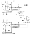
- FIG. 1 shows a circuit arrangement according to the prior art, to which two circuits S1 and S2 belonging to different logic families may belong, of which only one substitute image of the output stage is given.
- Circuit S1 may be an ECL circuit which is operated with supply voltages + 5V and OV (ground) and which has a constant current source connected to the supply voltage + 5V at its complementary outputs. The current provided by the respective constant current source thus has a direction (positive direction) pointing out of the circuit.
- the circuit S2 is operated with the supply voltages + 5V and OV, at the complementary outputs of which there is a constant current source connected to the OV, which provides a current with a direction pointing into the circuit (negative direction).
- the circuits S1 and S2 are each connected via two outputs to a pair of lines LP1 and LP2, the two lines of which each have a characteristic impedance Zo.
- the respective line pair is terminated by two terminating resistors Zo connected to one another, with connection point A of the terminating resistors in the case of line pair LP1 is connected to ground (0V) via a resistor R1 and a capacitor (not shown).
- connection point B of the terminating resistors Zo is connected to + 5V via a resistor R2 and to ground via a capacitor (not shown). High resistances occur at the resistors, especially when the line impedances are low.
- the capacitors just mentioned are only used to suppress high-frequency interference signals at the connection points mentioned.
- FIG. 1 The aforementioned high power losses occurring in the prior art are avoided by a circuit arrangement shown in FIG.
- This circuit arrangement essentially corresponds to the circuit arrangement shown in FIG. The only difference is that the connection points A and B of the terminating resistors Zo are now connected to one another via a resistor R3.
- resistor R1 the power loss originally occurring at resistor R1 (FIG. 1) is distributed between resistor R3 and the outputs of circuit S2 with the associated terminating resistors.
- the circuit S1 For the entire output-side wiring of the circuits S1 and S2, only the same power is required as for the circuit S1 in the conventional circuit shown in FIG. 1 alone.
- FIG. 2 it is assumed as an example that a total current is supplied to the resistor R3 from the circuit S1 which exceeds the total current that can be absorbed by the circuit S2.
- the circuit S1 supplies a total current of 28 mA, while the circuit S2 can only absorb a total current of 16 mA.
- a further resistor R4 connected to ground is connected to the connection point B, via which the differential current can flow off.
- the resistor R4 can be connected via the connection point B or A, for example, to the supply voltage of the circuit S1 (+ 5V) .
- this resistor R4 is connected with one of its connections to the resistor R3, while the remaining connection is connected to ground or one of the supply voltages of the circuits S1 and S2 in such a way that the current balance between the total current supplied to the resistor R3 and the outflowing total current is balanced.
- the resistance values for Zo are set at 50 ⁇ , for R3 at 46 ⁇ and for R4 at 140 ⁇ .
- the circuit arrangement according to FIG. 2 can also be modified such that a plurality of circuits corresponding to circuit S1 are connected to connection point A and a plurality of circuits corresponding to circuit S2 are connected to connection point B.
- Such a combination of several circuits at the connection points A and B further improves the power loss balance of the entire circuit arrangement because the current sums at A and B can be better balanced.
- connection points A and B can also be split into subnodes and spatially distributed in order to be able to connect the individual spatially separate circuits to the connection points A and B.
- the individual subnodes In differential operation the individual subnodes generally remain at a sufficiently constant potential. However, should this constancy not be sufficient under certain conditions, for example due to the scattering of high-frequency signals, the individual distributed subnodes could be supported with the capacitors corresponding to the capacitors shown in FIG.
- the present invention cannot be used only for a combination of circuits, as indicated in FIG. 2. Rather, it is generally applicable whenever circuits of different logic families are provided and the output stages of which have constant current sources which supply constant currents in different directions and which are terminated with a fixed terminating resistor. These circuits can be designed for the delivery of differential output signals as well as for the delivery of non-differential output signals. In the latter, high-pass limited signals with sufficient support by capacitors according to FIG 2 are required.
Landscapes
- Engineering & Computer Science (AREA)
- Power Engineering (AREA)
- Computer Networks & Wireless Communication (AREA)
- Signal Processing (AREA)
- Computer Hardware Design (AREA)
- Physics & Mathematics (AREA)
- Computing Systems (AREA)
- General Engineering & Computer Science (AREA)
- Mathematical Physics (AREA)
- Logic Circuits (AREA)
- Dc Digital Transmission (AREA)
Applications Claiming Priority (2)
| Application Number | Priority Date | Filing Date | Title |
|---|---|---|---|
| DE19944430053 DE4430053C1 (de) | 1994-08-24 | 1994-08-24 | Schaltungsanordnung mit mindestens zwei, unterschiedlichen Logikfamilien zugehörigen Schaltkreisen |
| DE4430053 | 1994-08-24 |
Publications (2)
| Publication Number | Publication Date |
|---|---|
| EP0698967A2 true EP0698967A2 (fr) | 1996-02-28 |
| EP0698967A3 EP0698967A3 (fr) | 2000-02-23 |
Family
ID=6526468
Family Applications (1)
| Application Number | Title | Priority Date | Filing Date |
|---|---|---|---|
| EP95113041A Withdrawn EP0698967A3 (fr) | 1994-08-24 | 1995-08-18 | Circuit associant au moins deux familles logique différentes |
Country Status (2)
| Country | Link |
|---|---|
| EP (1) | EP0698967A3 (fr) |
| DE (1) | DE4430053C1 (fr) |
Cited By (1)
| Publication number | Priority date | Publication date | Assignee | Title |
|---|---|---|---|---|
| CN1108593C (zh) * | 1996-08-29 | 2003-05-14 | 瑞士电信流动电话公司 | -数据载体卡加载或续加载-钱款值的方法 |
Families Citing this family (1)
| Publication number | Priority date | Publication date | Assignee | Title |
|---|---|---|---|---|
| DE19742430A1 (de) * | 1997-09-25 | 1999-04-08 | Siemens Ag | Datenübertragungssystem |
Family Cites Families (3)
| Publication number | Priority date | Publication date | Assignee | Title |
|---|---|---|---|---|
| EP0129542A4 (fr) * | 1982-12-27 | 1986-06-11 | Storage Technology Partners | Circuit cmos utilisant des interconnexions de lignes de transmission. |
| US5023488A (en) * | 1990-03-30 | 1991-06-11 | Xerox Corporation | Drivers and receivers for interfacing VLSI CMOS circuits to transmission lines |
| US5120998A (en) * | 1991-03-04 | 1992-06-09 | Motorola, Inc. | Source terminated transmission line driver |
-
1994
- 1994-08-24 DE DE19944430053 patent/DE4430053C1/de not_active Expired - Fee Related
-
1995
- 1995-08-18 EP EP95113041A patent/EP0698967A3/fr not_active Withdrawn
Non-Patent Citations (1)
| Title |
|---|
| None |
Cited By (1)
| Publication number | Priority date | Publication date | Assignee | Title |
|---|---|---|---|---|
| CN1108593C (zh) * | 1996-08-29 | 2003-05-14 | 瑞士电信流动电话公司 | -数据载体卡加载或续加载-钱款值的方法 |
Also Published As
| Publication number | Publication date |
|---|---|
| EP0698967A3 (fr) | 2000-02-23 |
| DE4430053C1 (de) | 1995-10-05 |
Similar Documents
| Publication | Publication Date | Title |
|---|---|---|
| DE69215403T2 (de) | Vorrichtung zur Verbindung einer Last an einer Stromversorgung | |
| DE3311881C2 (fr) | ||
| EP0300261A1 (fr) | Commutateur à diodes p-i-n | |
| DE19982963B4 (de) | Dynamische Vorspannungsschaltung, die eine frühe Spannungsklemmschaltung und translineare Techniken benutzt | |
| DE4135471A1 (de) | Kabelverbindung zwischen einem pc und einer naehmaschine | |
| DE2827067C2 (de) | Logikschaltung | |
| DE68922762T2 (de) | Schaltungsvorrichtung mit geringer Absorption zum Steuern eines Leistungstransistors. | |
| DE69426720T2 (de) | Halbleiterschaltungsanordnung mit einer Kombination von CMOS- und bipolaren Schaltungen | |
| EP0698967A2 (fr) | Circuit associant au moins deux familles logique différentes | |
| DE3010267C2 (fr) | ||
| DE19501236A1 (de) | Verstärker | |
| DE10314514B4 (de) | Leistungsvorrichtungssteuerschaltung | |
| EP0057239A1 (fr) | Circuit d'attaque du type push-pull monolithiquement intégré | |
| EP1318594B1 (fr) | Circuit convertisseur de puissance pour augmentation d'une tension alternative | |
| DE3145771C2 (fr) | ||
| EP0370576A2 (fr) | Oscillateur | |
| EP1038355B1 (fr) | Circuit tampon | |
| EP0133618A1 (fr) | Circuit oscillateur haute fréquence à quartz sous forme de circuit intégré monolithique | |
| DE10127868A1 (de) | Bootstrap-Spannungsversorgung | |
| EP0588111B1 (fr) | Elément de mémoire | |
| EP0624802B1 (fr) | Circuit pour le redressement de signaux de tension alternative | |
| EP0889584A2 (fr) | Circuit de commutation et d'accord comportant des branches de filtrage, à gamme de fréquences différente, connecteés en parallèle | |
| EP0763867A1 (fr) | Dispositif de transmission de signaux par des lignes triplaques | |
| DE10200518A1 (de) | Spannungsbegrenzer für den Schnittstellenkreis eines Kommunikationsbusses | |
| DE3427542A1 (de) | Schaltungsanordnung zur einstellung des emitterstromes einer transistorverstaerkerstufe |
Legal Events
| Date | Code | Title | Description |
|---|---|---|---|
| PUAI | Public reference made under article 153(3) epc to a published international application that has entered the european phase |
Free format text: ORIGINAL CODE: 0009012 |
|
| AK | Designated contracting states |
Kind code of ref document: A2 Designated state(s): AT BE CH DK FR GB IT LI NL SE |
|
| PUAL | Search report despatched |
Free format text: ORIGINAL CODE: 0009013 |
|
| AK | Designated contracting states |
Kind code of ref document: A3 Designated state(s): AT BE CH DK FR GB IT LI NL SE |
|
| RIC1 | Information provided on ipc code assigned before grant |
Free format text: 7H 03K 19/00 A, 7H 04L 25/02 B, 7G 06F 13/40 B |
|
| STAA | Information on the status of an ep patent application or granted ep patent |
Free format text: STATUS: THE APPLICATION IS DEEMED TO BE WITHDRAWN |
|
| 18D | Application deemed to be withdrawn |
Effective date: 20000301 |