EP0699005B1 - Numerische Datenkonvertierung - Google Patents
Numerische Datenkonvertierung Download PDFInfo
- Publication number
- EP0699005B1 EP0699005B1 EP95305585A EP95305585A EP0699005B1 EP 0699005 B1 EP0699005 B1 EP 0699005B1 EP 95305585 A EP95305585 A EP 95305585A EP 95305585 A EP95305585 A EP 95305585A EP 0699005 B1 EP0699005 B1 EP 0699005B1
- Authority
- EP
- European Patent Office
- Prior art keywords
- clock
- data
- period
- digital data
- circuit
- Prior art date
- Legal status (The legal status is an assumption and is not a legal conclusion. Google has not performed a legal analysis and makes no representation as to the accuracy of the status listed.)
- Expired - Lifetime
Links
Images


Classifications
-
- G—PHYSICS
- G11—INFORMATION STORAGE
- G11B—INFORMATION STORAGE BASED ON RELATIVE MOVEMENT BETWEEN RECORD CARRIER AND TRANSDUCER
- G11B20/00—Signal processing not specific to the method of recording or reproducing; Circuits therefor
- G11B20/10—Digital recording or reproducing
-
- H—ELECTRICITY
- H03—ELECTRONIC CIRCUITRY
- H03H—IMPEDANCE NETWORKS, e.g. RESONANT CIRCUITS; RESONATORS
- H03H17/00—Networks using digital techniques
- H03H17/02—Frequency selective networks
- H03H17/06—Non-recursive filters
- H03H17/0621—Non-recursive filters with input-sampling frequency and output-delivery frequency which differ, e.g. extrapolation; Anti-aliasing
- H03H17/0628—Non-recursive filters with input-sampling frequency and output-delivery frequency which differ, e.g. extrapolation; Anti-aliasing the input and output signals being derived from two separate clocks, i.e. asynchronous sample rate conversion
-
- H—ELECTRICITY
- H04—ELECTRIC COMMUNICATION TECHNIQUE
- H04N—PICTORIAL COMMUNICATION, e.g. TELEVISION
- H04N9/00—Details of colour television systems
- H04N9/79—Processing of colour television signals in connection with recording
- H04N9/87—Regeneration of colour television signals
-
- H—ELECTRICITY
- H04—ELECTRIC COMMUNICATION TECHNIQUE
- H04N—PICTORIAL COMMUNICATION, e.g. TELEVISION
- H04N9/00—Details of colour television systems
- H04N9/79—Processing of colour television signals in connection with recording
- H04N9/80—Transformation of the television signal for recording, e.g. modulation, frequency changing; Inverse transformation for playback
- H04N9/82—Transformation of the television signal for recording, e.g. modulation, frequency changing; Inverse transformation for playback the individual colour picture signal components being recorded simultaneously only
- H04N9/83—Transformation of the television signal for recording, e.g. modulation, frequency changing; Inverse transformation for playback the individual colour picture signal components being recorded simultaneously only the recorded chrominance signal occupying a frequency band under the frequency band of the recorded brightness signal
Definitions
- This invention relates to converting digital data. More particularly, but not exclusively, the invention relates to converting circuits and methods for a sampling phase of digital data.
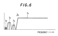
- a luminance signal is converted into an FM signal SY during a recording operation (see Fig. 6). Further, a carrier color signal SC is frequency-converted into a lower band side of the FM luminance signal, and an audio signal is converted into an FM signal SA in a band between the signal SC and the signal SY. Then, a frequency multiplexed signal SF produced from these signals SY, SC, SA and a tracking servo pilot signal SP is recorded on a magnetic tape by way of a rotary magnetic head in such a manner that a 1-field signal SF becomes one inclined magnetic track on this magnetic tape.
- this signal reproducing system may be arranged as shown in, for example, Fig. 7. That is, the frequency multiplexed signal SF is continuously reproduced from the magnetic tape 1 by the rotary magnetic heads 11A and 11B.
- the reproduced signal SF is supplied via the reproducing amplifier 12 to the servo circuit 41, so that the tracking servo control for the heads 11A and 11B with respect to the tracks of the magnetic tape 1 is carried out in response to the pilot signal SP contained in the signal SF.
- the signal SF derived from the amplifier 12 is supplied to the bandpass filter 13 so as to derive the FM luminance signal SY.
- This FM luminance signal SY is supplied to the A/D converter 14 in order to be A/D-converted into, for instance, an 8-bit digital signal for 1 sample, whose sampling frequency is eight times higher than the color subcarrier frequency fSC (approximately 3.58MHz). Then, this 8-bit digital signal SY is supplied to the processing circuit 15 in which such process operations as FM demodulation and deemphasis are carried out. Then, the processed signal SY is supplied to the D/A converter 16 so as to be D/A-converted into the original baseband luminance signal Y which will then be derived from the terminal 17.
- the signal SF derived from the amplifier 12 is supplied to the bandpass filter 21, thereby deriving the color carrier signal SC.
- This color carrier signal SC is supplied to the A/D converter 22 so as to be A/D-converted into, for instance, an 8-bit digital signal SC for 1 sample, having a sampling frequency four times higher than the color subcarrier frequency.
- this 8-bit digital signal SC is supplied to the processing circuit 23 so that such processing operations as APC and eliminations of track crosstalk components are carried out, and this digital signal SC is color-demodulated into the baseband red and blue color difference signals (R-Y) and (B-Y).
- These color difference signal (R-Y) and (B-Y) are supplied via the converting circuit (will be discussed later) 24 to the NTSC encoder 25 in which the color subcarrier frequency is encoded into the color carrier signal SS having the frequency fSC.
- This color carrier signal SS is supplied into the D/A-converter 26 so as to be D/A-converted into the original color carrier signal SS, which will then be derived from the terminal 27.
- both of the luminance signal Y derived from the D/A converter 16 and the color carrier signal SS derived from the D/A converter 26 are supplied to the adding circuit 18, so that the NTSC composite signal is synthesized which will then be derived from the terminal 19.
- the signal SF from the amplifier 12 is furnished to the audio processing circuit 31, so that the original audio signals "L” and “R” are demodulated from the FM audio signal SA contained in this signal SF. These original audio signals are derived from the terminal 32.
- both of the reproduced FM luminance signal SY and color carrier signal SC contain variations in a time axis such as "jitter". Also, the time axis is changed when the VTR signal is reproduced at varied speeds.
- the clock thereof is produced from the horizontal sync signal contained in the reproduced FM luminance signal SY.
- various variations are produced in the sampling phases (namely, phase at time instant when data is obtained) among the luminance signals Y outputted from the processing circuit 15, and the color difference signals (R-Y), (B-Y) outputted from the processing circuits 23, 24.
- the circuit for stabilizing the sampling phases and for aligning the sampling phases of the color difference signals (R-Y) and (B-Y) derived from the processing circuit 23 is the converting circuit 24. That is to say, the converting circuit 24 is to convert the sampling phases of the color difference signals (digital data) derived from the processing circuit 23 into the clock phases of the encoder 25 even when the processing circuit 23 is operated in asynchronism with the encoder 25.
- the signal recording system similarly requires such a converting circuit for stabilizing and aligning the sampling phases in the digital processing circuit for the color carrier signal due to the same jitter reason.
- a conventional time base corrector circuit is disclosed in EP-A-292 108.
- the invention provides a converting circuit as set out in claim 1 and a converting method as set out in claim 5.
- a preferred embodiment of the invention described hereinbelow provides a converting circuit (50) and method for converting first digital data (DIN) synchronized with a first clock (CK) into second digital data (D OUT) synchronized with a second clock (XCK) not synchronized with the first clock (CK), in which 1 (one) time period of the first clock (CK) is divided into N time periods ("N" being larger than or equal to 2), first and second interpolation coefficients (KA, KB) are set with respect to each of the divided time periods, and the second digital data D OUT is produced from data (n+1) within a certain clock period and data (n+2) within another clock period subsequent to said certain clock period among the first digital data (DI), by using the first and second interpolation coefficients (KA, KB) in the divided period where the second clock (XCK) is located, among the first and second interpolation coefficients (KA, KB) set for each of the divided periods.
- the first digital data is converted, in the preferred embodiment, into digital data having a sampling frequency equivalently N times higher than that of the first digital data.
- the data at the second clock position among then are derived as a converted output.
- the sampling phase of the input data (DIN) can be converted.
- the input data DIN is sampled at the clock having, for instance, a frequency four times higher than that of the clock frequency, so that the sampling phase may be equivalently converted.
- this phase difference can be limited to a small range.
- the clock (XCK) passes over the clock (CK), or is delayed from this clock (CK), distortion occurring in the output data (D OUT) can be reduced.
- the bandwidth of the sampling frequency may have margin with respect to that of the input data (DIN). Even when a filter having a lesser number of taps is employed, deterioration in frequency characteristics may be suppressed.
- the preferred embodiment thus provides a converting circuit (and method) for converting a sampling phase of digital data. More specifically, the preferred embodiment provides a converting circuit with a simple structure, whose characteristic is better than that of the above-described previously proposed converting circuit.
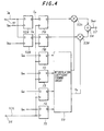
- reference numeral 50 indicates an example of a circuit for converting a sampling phase of digital data.
- This converting circuit 50 corresponds to, for instance, the converting circuit for converting either the color difference signal (R-Y), or the color difference signal (B-Y) in the converting circuit 24 of Fig. 6.
- digital data "DIN" to be converted is supplied via a terminal 51 to D-inputs of D flip-flop circuits 52A and 52B.
- the data DIN for instance, such parallel data is employed that 1 sample is equal to 8 bits. Accordingly, these flip-flop circuits 52A and 52B own 8-bit inputs/outputs, respectively. Also, for instance, as shown in Fig. 2A, it is assumed that 1 sample period (namely, 1 clock period) of the data DIN is a value of " ⁇ ", and also the sampling numbers of the data DIN are n, n+1, n+2, ....
- a clock "CK" is supplied to a terminal 61.
- this clock CK corresponds to such a pulse formed by supplying the horizontal sync (synchronization) signal to the PLL (phase-locked loop).
- this clock CK is synchronized with the data DIN.
- this clock CK is supplied via the terminal 61 to a T flip- flop circuit 62.
- the clock CK is inverted every 1 sampling period " ⁇ ", and also two pulses "Q62" and "Q62! whose phases are opposite to each other are derived. These pulses Q62 and Q62! are supplied to the flip-flop circuits 52A and 52B as clocks thereof.
- even-numbered sample data DA among the data DIN are derived from the flip-flop circuit 52A in a time period equal to the period "2 ⁇ ".
- odd-numbered sample data DB among the data DIN are derived in a time period equal to the period "2 ⁇ , and are delayed from the first-mentioned data DA by a period " ⁇ ".
- the pulse Q62 derived from the flip-flop circuit 62 is supplied to the D input of the D flip-flop circuit 63, and the clock CK from the terminal 61 is supplied to an invertor 63, so that a pulse Q63 whose phase is inverted is produced from this invertor 63, as shown in Fig. 2G.
- This pulse Q63 is supplied as a clock to the flip-flop circuit 64.
- a pulse Q64 is derived from the flip-flop circuit 64, which is inverted at each of the central time instants of the respective samples of the data DIN.
- the pulse Q63 derived from the inverter 63 is supplied to a delay circuit 65, so that as illustrated in Fig. 2I, a pulse Q65 is produced which is delayed by a time period of 1/4 ⁇ from the pulse Q63. Then, this pulse Q65 is supplied to an AND (gate) circuit 66, and also the pulse Q64 from the flip-flop circuit 64 is supplied to this AND circuit 66. As represented in Fig. 2J, a pulse Q66 is derived from this AND circuit 66, which has a rising portion at the central 1/2 ⁇ period of the even-numbered data DA. Then, this pulse Q66 is supplied to an interpolation coefficient forming circuit 69.
- the pulse Q65 from the delay circuit 65 is furnished to an AND circuit 67, and also the pulse Q64 from the flip-flop circuit 64 is supplied to a negative logic input of the AND circuit 67. From this AND circuit 67, as indicated in Fig. 2K, a pulse Q67 is derived which has a rising portion at the central 1/2 ⁇ period of the odd-numbered data DB. Then, this pulse Q67 is supplied to the interpolation forming circuit 69.
- the pulse Q66 from the AND circuit 66 is supplied to a D-input of a D flip-flop circuit 68, and the clock CK from the terminal 61 is furnished to the flip-flop circuit 68 as a clock thereof.
- a pulse Q68 which is inverted at the changing points of the data DA and DB is derived from the flip-flop circuit 68.
- this pulse Q68 is supplied to the interpolation coefficient forming circuit 69.
- the pulse Q63 derived from the inverter 63 is also supplied to this interpolation coefficient forming circuit 69.
- the pulses Q68, Q66, Q67, and Q63 are supplied to the interpolation forming circuit 69.
- a time period obtained when these pulses Q68 to Q63 are combined with each other is equal to a time period "2 ⁇ ".
- the time period "2 ⁇ " of the sample numbers n+1 and n+2 of the data DIN is equally divided by 1/8 every time period of 1/4 ⁇ . These divided time periods are successively defined as time periods T1 to T8.
- interpolation coefficients KA and KB are derived from the interpolation coefficient forming circuit 69, and these interpolation coefficients KA, KB own values which are complementary changed by 1/4 every periods of 1/4 ⁇ within the time periods T1 to T8.
- the data DA and DB from the flip-flop circuits 52A and 52B are supplied to multiplier circuits 53A and 53B, and also the coefficients KA, KB from the interpolation coefficient forming circuit 69 are supplied to the multiplier circuits 53A and 53B, so that these coefficients KA and KB are multiplied with the data DA and DB.
- the data D54 during the respective clock periods ⁇ becomes such data that the ratio of the preceding sample to the data DIN is gradually decreased every 1/4 ⁇ time period, and the ratio of the succeeding sample to the data DIN is gradually increased every 1/4 ⁇ time period. Consequently, for example, as illustrated by a solid line in Fig. 20 (this implies D/A-converted waveform), the data D54 owns such a waveform that the data DIN is linear-interpolated, and is changed every 1/4 ⁇ time period.
- this data D54 is supplied to a D-input of a D flip-flop circuit 55, and further, as shown in Fig. 2p, a clock XCK produced after the sampling phase has been converted is supplied as a clock from a terminal 56 to the flip-flop circuit 55.
- this clock XCK corresponds to a signal having a stable frequency and a stable phase, which has been formed in a crystal oscillator circuit.
- the data Q54 is latched every clock XCK in the flip-flop circuit 55, so that latched data D OUT is derived from the terminal 57.
- this data D OUT must be equal to such data that the sampling phase of the input data DIN is converted into the phase of the clock XCK.
- the sampling phase of the input data DIN may be converted by this converting circuit 50.
- this converting circuit 50 such an equivalent operation is achieved that the input data DIN is sampled at the clock 4 times higher than this input data to convert the sampling phase.
- this phase difference may be limited to a small range.
- the clock XCK passes over the clock CK, or is delayed from the clock CK, distortion occurred in the output data D OUT may be reduced.
- the bandwidth of the sampling frequency may have margin with respect to that of the input data DIN. Even when a filter having a less number of taps is employed, deterioration in the frequency characteristics may be suppressed.
- the data at the time instants of the clock XCK among the data D54 synthesized in the adder circuit 54 is latched in the D flip-flop circuit 55 to obtain the output data D OUT, whereas in the example indicated in Fig. 4, the respective data before being synthesized in the adder circuit are latched to obtain the output data D OUT.
- the data DA and DB derived from the D flip-flop circuits 52A and 52B are supplied to D flip-flop circuits 71A and 71B, and also the clock XCK is furnished to the D flip-flop circuits 71A and 71B as clock inputs thereof.
- the data at the rising time instants of the clock XCK among the data DA and DB are latched by the D flip-flop circuits 71A and 71B during this clock time period.
- These latched data DA and DB are supplied to multiplier circuits 53A and 53B.
- the pulses Q68, Q66, Q67, Q63 are supplied through D flip-flop circuits 72 to 75 to the interpolation coefficient forming circuit 69, and further the clock XCK is supplied to the D flip-flop circuits 72 to 75.
- the coefficients KA and KB at the rising time of the clock XCK, namely the time period within the time periods T11 to T8, where the rising portion of the clock XCK is present, are supplied to the multiplier circuits 53A and 53B during this clock time period.
- the pulses Q68, Q66, Q67, Q63 at the rising time of the clock XCK are latched by the D flip-flop circuits 72 to 75 until the rising portion of the subsequent clock XCK. Then, this latched result is supplied to a phase judging circuit 76.
- the phase judging circuit 76 judges that these pulses Q68, Q66, Q67, Q63 belong to any one of these time periods T1 to T8, and holds the judgment result during the time period of the clock XCK.
- this judgment result is supplied to the interpolation coefficient forming circuit 69 to derive the coefficients KA and KB corresponding to the time period judged from the time periods T1 to T8.
- These derived coefficients KA and KB are supplied to the multiplier circuits 53A and 53B, respectively.
- data D OUT that the sampling phase has been converted at the time instant of the clock XCK is outputted from the adder circuit 54, and the resultant data is derived to the terminal 57.
- the coefficients KA and KB for linear-interpolating the data DA and DB have been formed in the interpolation coefficient circuit 69 in the above description, these coefficients KA and KB may be substituted by interpolation coefficients by other functions. In such a case that the levels of the data DA and DB are not stable during the time periods T4, T5, T8 and T1, the data may be substituted by, for instance, one preceding sample.
- the delay circuit 65 may be constructed of an analog circuit, or a digital circuit by using a counter.
Landscapes
- Engineering & Computer Science (AREA)
- Signal Processing (AREA)
- Multimedia (AREA)
- Physics & Mathematics (AREA)
- Computer Hardware Design (AREA)
- Mathematical Physics (AREA)
- Analogue/Digital Conversion (AREA)
- Signal Processing For Digital Recording And Reproducing (AREA)
- Processing Of Color Television Signals (AREA)
Claims (7)
- Konvertierungsschaltung zum Konvertieren von ersten digitalen Daten (D IN), die mit einem ersten Taktsignal (CK) synchronisiert sind, in zweite digitale Daten (D OUT), die mit einem zweiten Taktsignal (XCK) synchronisiert sind, welches nicht mit dem ersten Taktsignal synchronisiert ist, miteiner Teilerschaltung zum Unterteilen eines Zeitintervalls des ersten Taktsignals in N Zeitintervalle (T1 .... T8), wobei N größer oder gleich 2 ist;einer Koeffizienten-Einstellschaltung (69) zum Einstellen eines ersten (KA) und eines zweiten (KB) Interpolationskoeffizienten bezüglich jedes der unterteilten Zeitintervalle;einer Datenerzeugungsschaltung (52A, 52B, 53A, 53B, 54, 55) zum Erzeugen der zweiten digitalen Daten von Daten in einem bestimmten Taktintervall und von Daten in einem anderen, dem bestimmten Taktintervall anschließenden Taktintervall aus den ersten digitalen Daten durch darauf Anwenden des ersten und des zweiten Interpolationskoeffizienten, die dem unterteilten Intervall entsprechen, in dem das zweite Taktsignal vorliegt, und die unter den ersten und zweiten Interpolationskoeffizienten ausgewählt sind, die für jedes der unterteilten Intervalle eingestellt sind.
- Konvertierungsschaltung nach Anspruch 1,
dadurch gekennzeichnet,daß digitale Daten mit einer Taktfrequenz viermal so groß wie die des Taktsignals basierend auf den Daten in dem bestimmten Intervall und den Daten in dem dem bestimmten Intervall anschließenden Intervall unter den ersten digitalen Daten für jedes der unterteilten Intervalle durch Benutzung des ersten und des zweiten Interpolationskoeffizienten in dem unterteilten Intervall erzeugt werden; unddaß die Daten in dem unterteilten Intervall, in dem das zweite Taktsignal vorliegt, unter den erzeugten digitalen Daten abgeleitet werden, um die zweiten digitalen Daten zu erzeugen. - Konvertierungsschaltung nach Anspruch 1,
dadurch gekennzeichnet,daß der erste und der zweite Interpolationskoeffizient in dem unterteilten Intervall unter den unterteilten Intervallen, in dem das zweite Taktsignal vorliegt, abgeleitet werden; unddaß die zweiten digitalen Daten aus den Daten in dem bestimmten Taktintervall und den Daten in dem dem bestimmten Taktintervall anschließenden Taktintervall unter den ersten digitalen Daten durch Verwendung des abgeleiteten ersten und zweiten Interpolationskoeffizienten erzeugt werden. - Konvertierungsschaltung nach einem der Ansprüche 1, 2 oder 3,
dadurch gekennzeichnet,
daß die Konvertierungsschaltung eine Konvertierungsschaltung einer Abtastphase von derartigen digitalen Daten ist, daß N = 4 gilt. - Verfahren zum Konvertieren von ersten digitalen Daten, die mit einem ersten Taktsignal synchronisiert sind, in zweite digitale Daten, die mit einem zweiten Taktsignal synchronisiert sind, welches nicht mit dem ersten Taktsignal synchronisiert ist, mit den Verfahrensschritten:Unterteilen eines Zeitintervalls des ersten Taktsignals in N Zeitintervalle, wobei N größer oder gleich 2 ist;Einstellen eines ersten und eines zweiten Interpolationskoeffizienten bezüglich jedes der unterteilten Zeitintervalle;Erzeugen der zweiten digitalen Daten von Daten in einem bestimmten Taktintervall und von Daten in einem anderen, dem bestimmten Taktintervall anschließenden Taktintervall aus den ersten digitalen Daten durch darauf Anwenden des ersten und des zweiten Interpolationskoeffizienten, die dem unterteilten Intervall entsprechen, in dem das zweite Taktsignal vorliegt, und die unter den ersten und zweiten Interpolationskoeffizienten ausgewählt sind, die für jedes der unterteilten Intervalle eingestellt sind.
- Konvertierungsverfahren nach Anspruch 5,
dadurch gekennzeichnet,daß digitale Daten mit einer Taktfrequenz viermal so groß wie die des Taktsignals basierend auf den Daten in dem bestimmten Intervall und den Daten in dem dem bestimmten Intervall anschließenden Intervall unter den ersten digitalen Daten für jedes der unterteilten Intervalle durch Benutzung des ersten und des zweiten Interpolationskoeffizienten in dem unterteilten Intervall erzeugt werden; unddaß die Daten in dem unterteilten Intervall, in dem das zweite Taktsignal vorliegt, unter den erzeugten digitalen Daten abgeleitet werden, um die zweiten digitalen Daten zu erzeugen. - Konvertierungsverfahren nach Anspruch 5,
dadurch gekennzeichnet,daß der erste und der zweite Interpolationskoeffizient in dem unterteilten Intervall unter den unterteilten Intervallen, in dem das zweite Taktsignal vorliegt, abgeleitet werden; unddaß die zweiten digitalen Daten aus den Daten in dem bestimmten Taktintervall und den Daten in dem dem bestimmten Taktintervall anschließenden Taktintervall unter den ersten digitalen Daten durch Verwendung des abgeleiteten ersten und zweiten Interpolationskoeffizienten erzeugt werden.
Applications Claiming Priority (3)
| Application Number | Priority Date | Filing Date | Title |
|---|---|---|---|
| JP21210794 | 1994-08-12 | ||
| JP21210794A JP3528868B2 (ja) | 1994-08-12 | 1994-08-12 | デジタルデータのサンプリング位相の変換回路 |
| JP212107/94 | 1994-08-12 |
Publications (3)
| Publication Number | Publication Date |
|---|---|
| EP0699005A2 EP0699005A2 (de) | 1996-02-28 |
| EP0699005A3 EP0699005A3 (de) | 1997-04-16 |
| EP0699005B1 true EP0699005B1 (de) | 2000-03-01 |
Family
ID=16617001
Family Applications (1)
| Application Number | Title | Priority Date | Filing Date |
|---|---|---|---|
| EP95305585A Expired - Lifetime EP0699005B1 (de) | 1994-08-12 | 1995-08-10 | Numerische Datenkonvertierung |
Country Status (5)
| Country | Link |
|---|---|
| US (1) | US5870038A (de) |
| EP (1) | EP0699005B1 (de) |
| JP (1) | JP3528868B2 (de) |
| KR (1) | KR100353098B1 (de) |
| DE (1) | DE69515234T2 (de) |
Families Citing this family (5)
| Publication number | Priority date | Publication date | Assignee | Title |
|---|---|---|---|---|
| KR100264376B1 (ko) * | 1996-04-04 | 2000-08-16 | 가나이 쓰도무 | 디지탈 기록방식의 비디오카메라장치 |
| KR100541053B1 (ko) * | 2003-02-11 | 2006-01-10 | 삼성전자주식회사 | 프로세스들간의 출력 동기가 보정된 다중 프로세스 a/d컨버터 |
| US6809664B1 (en) * | 2003-06-26 | 2004-10-26 | International Business Machines Corporation | Double width data bus, single rate to single width data bus, double rate converter circuit |
| JP2009500997A (ja) * | 2005-07-08 | 2009-01-08 | メド−エル エレクトロメディジニシェ ゲラテ ゲーエムベーハー | Cmos全波整流器 |
| US8248141B2 (en) | 2005-07-08 | 2012-08-21 | Med-El Elekromedizinische Geraete Gmbh | Data and power system based on CMOS bridge |
Family Cites Families (4)
| Publication number | Priority date | Publication date | Assignee | Title |
|---|---|---|---|---|
| US4864387A (en) * | 1987-04-10 | 1989-09-05 | Sony Corporation | PAL video time base corrector inverts color difference signal (V) axis |
| JP2731151B2 (ja) * | 1987-09-18 | 1998-03-25 | 株式会社東芝 | 位相情報検出回路 |
| US5301196A (en) * | 1992-03-16 | 1994-04-05 | International Business Machines Corporation | Half-speed clock recovery and demultiplexer circuit |
| US5774080A (en) * | 1994-12-15 | 1998-06-30 | Analog Devices, Incorporated | Reduced transistor-count data storage and multiplexing system |
-
1994
- 1994-08-12 JP JP21210794A patent/JP3528868B2/ja not_active Expired - Fee Related
-
1995
- 1995-08-09 US US08/513,130 patent/US5870038A/en not_active Expired - Fee Related
- 1995-08-10 DE DE69515234T patent/DE69515234T2/de not_active Expired - Fee Related
- 1995-08-10 EP EP95305585A patent/EP0699005B1/de not_active Expired - Lifetime
- 1995-08-11 KR KR1019950024770A patent/KR100353098B1/ko not_active Expired - Fee Related
Also Published As
| Publication number | Publication date |
|---|---|
| KR100353098B1 (ko) | 2003-01-06 |
| DE69515234T2 (de) | 2000-07-13 |
| US5870038A (en) | 1999-02-09 |
| JP3528868B2 (ja) | 2004-05-24 |
| EP0699005A3 (de) | 1997-04-16 |
| DE69515234D1 (de) | 2000-04-06 |
| EP0699005A2 (de) | 1996-02-28 |
| KR960008791A (ko) | 1996-03-22 |
| JPH0856369A (ja) | 1996-02-27 |
Similar Documents
| Publication | Publication Date | Title |
|---|---|---|
| US4719518A (en) | Magnetic recording apparatus for carrying out recording by selectively using one of two kinds of recording systems | |
| US4668999A (en) | Time base equalizer and corrector (TIBEC) for video tape or disk machines in playback modes | |
| EP0699005B1 (de) | Numerische Datenkonvertierung | |
| US4143396A (en) | Digital chrominance separating and processing system and method | |
| JPS6386980A (ja) | 周期ノイズ除去装置 | |
| US4809084A (en) | Apparatus for processing video signal | |
| JPS63194495A (ja) | 映像信号記録再生装置 | |
| CN100525472C (zh) | 磁带录像机信号处理电路 | |
| US4370672A (en) | Color subcarrier regenerator for slow down processor | |
| JPS60187195A (ja) | 映像信号の記録再生装置 | |
| EP0486300A2 (de) | Verarbeitungssystem für Videosignale | |
| JP2502499B2 (ja) | 映像信号処理装置 | |
| JPH04109782A (ja) | 画像信号処理装置 | |
| JPH0135557B2 (de) | ||
| JP2648041B2 (ja) | 映像信号処理回路 | |
| JPS61184085A (ja) | 映像信号処理方法 | |
| JP2614238B2 (ja) | 記録装置及び再生装置 | |
| JPS61203792A (ja) | 映像信号処理装置 | |
| JPH0250576A (ja) | 映像信号処理装置 | |
| JPH0681329B2 (ja) | 映像信号処理装置 | |
| JPS60224389A (ja) | 映像信号記録方式 | |
| JPH01300794A (ja) | 映像信号処理装置 | |
| JPS627758B2 (de) | ||
| JPS62224190A (ja) | 映像信号記録再生装置 | |
| JPH0666771B2 (ja) | 位相同期回路 |
Legal Events
| Date | Code | Title | Description |
|---|---|---|---|
| PUAI | Public reference made under article 153(3) epc to a published international application that has entered the european phase |
Free format text: ORIGINAL CODE: 0009012 |
|
| AK | Designated contracting states |
Kind code of ref document: A2 Designated state(s): DE FR GB |
|
| PUAL | Search report despatched |
Free format text: ORIGINAL CODE: 0009013 |
|
| AK | Designated contracting states |
Kind code of ref document: A3 Designated state(s): DE FR GB |
|
| 17P | Request for examination filed |
Effective date: 19970904 |
|
| GRAG | Despatch of communication of intention to grant |
Free format text: ORIGINAL CODE: EPIDOS AGRA |
|
| 17Q | First examination report despatched |
Effective date: 19990504 |
|
| GRAG | Despatch of communication of intention to grant |
Free format text: ORIGINAL CODE: EPIDOS AGRA |
|
| GRAH | Despatch of communication of intention to grant a patent |
Free format text: ORIGINAL CODE: EPIDOS IGRA |
|
| GRAH | Despatch of communication of intention to grant a patent |
Free format text: ORIGINAL CODE: EPIDOS IGRA |
|
| GRAA | (expected) grant |
Free format text: ORIGINAL CODE: 0009210 |
|
| AK | Designated contracting states |
Kind code of ref document: B1 Designated state(s): DE FR GB |
|
| REF | Corresponds to: |
Ref document number: 69515234 Country of ref document: DE Date of ref document: 20000406 |
|
| ET | Fr: translation filed | ||
| PLBE | No opposition filed within time limit |
Free format text: ORIGINAL CODE: 0009261 |
|
| STAA | Information on the status of an ep patent application or granted ep patent |
Free format text: STATUS: NO OPPOSITION FILED WITHIN TIME LIMIT |
|
| 26N | No opposition filed | ||
| REG | Reference to a national code |
Ref country code: GB Ref legal event code: IF02 |
|
| PGFP | Annual fee paid to national office [announced via postgrant information from national office to epo] |
Ref country code: DE Payment date: 20050804 Year of fee payment: 11 |
|
| PGFP | Annual fee paid to national office [announced via postgrant information from national office to epo] |
Ref country code: FR Payment date: 20050809 Year of fee payment: 11 |
|
| PGFP | Annual fee paid to national office [announced via postgrant information from national office to epo] |
Ref country code: GB Payment date: 20050810 Year of fee payment: 11 |
|
| PG25 | Lapsed in a contracting state [announced via postgrant information from national office to epo] |
Ref country code: DE Free format text: LAPSE BECAUSE OF NON-PAYMENT OF DUE FEES Effective date: 20070301 |
|
| GBPC | Gb: european patent ceased through non-payment of renewal fee |
Effective date: 20060810 |
|
| REG | Reference to a national code |
Ref country code: FR Ref legal event code: ST Effective date: 20070430 |
|
| PG25 | Lapsed in a contracting state [announced via postgrant information from national office to epo] |
Ref country code: GB Free format text: LAPSE BECAUSE OF NON-PAYMENT OF DUE FEES Effective date: 20060810 |
|
| PG25 | Lapsed in a contracting state [announced via postgrant information from national office to epo] |
Ref country code: FR Free format text: LAPSE BECAUSE OF NON-PAYMENT OF DUE FEES Effective date: 20060831 |