EP0700146A1 - Multiplicateur de tension avec tension de sortie stabilisée lineairement - Google Patents
Multiplicateur de tension avec tension de sortie stabilisée lineairement Download PDFInfo
- Publication number
- EP0700146A1 EP0700146A1 EP94830413A EP94830413A EP0700146A1 EP 0700146 A1 EP0700146 A1 EP 0700146A1 EP 94830413 A EP94830413 A EP 94830413A EP 94830413 A EP94830413 A EP 94830413A EP 0700146 A1 EP0700146 A1 EP 0700146A1
- Authority
- EP
- European Patent Office
- Prior art keywords
- voltage
- capacitor
- switch
- terminal
- output
- Prior art date
- Legal status (The legal status is an assumption and is not a legal conclusion. Google has not performed a legal analysis and makes no representation as to the accuracy of the status listed.)
- Granted
Links
- 239000003990 capacitor Substances 0.000 claims abstract description 44
- 230000006641 stabilisation Effects 0.000 claims abstract description 10
- 230000000295 complement effect Effects 0.000 claims description 6
- 230000010354 integration Effects 0.000 claims description 5
- 238000010586 diagram Methods 0.000 description 6
- 230000033228 biological regulation Effects 0.000 description 3
- 238000011105 stabilization Methods 0.000 description 3
- 230000006870 function Effects 0.000 description 2
- 238000000034 method Methods 0.000 description 2
- 238000010521 absorption reaction Methods 0.000 description 1
- 230000002238 attenuated effect Effects 0.000 description 1
- 230000003247 decreasing effect Effects 0.000 description 1
- 230000003828 downregulation Effects 0.000 description 1
- 230000015654 memory Effects 0.000 description 1
- 230000002123 temporal effect Effects 0.000 description 1
Images


Classifications
-
- H—ELECTRICITY
- H02—GENERATION; CONVERSION OR DISTRIBUTION OF ELECTRIC POWER
- H02M—APPARATUS FOR CONVERSION BETWEEN AC AND AC, BETWEEN AC AND DC, OR BETWEEN DC AND DC, AND FOR USE WITH MAINS OR SIMILAR POWER SUPPLY SYSTEMS; CONVERSION OF DC OR AC INPUT POWER INTO SURGE OUTPUT POWER; CONTROL OR REGULATION THEREOF
- H02M3/00—Conversion of DC power input into DC power output
- H02M3/02—Conversion of DC power input into DC power output without intermediate conversion into AC
- H02M3/04—Conversion of DC power input into DC power output without intermediate conversion into AC by static converters
- H02M3/06—Conversion of DC power input into DC power output without intermediate conversion into AC by static converters using resistors or capacitors, e.g. potential divider
- H02M3/07—Conversion of DC power input into DC power output without intermediate conversion into AC by static converters using resistors or capacitors, e.g. potential divider using capacitors charged and discharged alternately by semiconductor devices with control electrode, e.g. charge pumps
-
- H—ELECTRICITY
- H02—GENERATION; CONVERSION OR DISTRIBUTION OF ELECTRIC POWER
- H02M—APPARATUS FOR CONVERSION BETWEEN AC AND AC, BETWEEN AC AND DC, OR BETWEEN DC AND DC, AND FOR USE WITH MAINS OR SIMILAR POWER SUPPLY SYSTEMS; CONVERSION OF DC OR AC INPUT POWER INTO SURGE OUTPUT POWER; CONTROL OR REGULATION THEREOF
- H02M1/00—Details of apparatus for conversion
- H02M1/0045—Converters combining the concepts of switch-mode regulation and linear regulation, e.g. linear pre-regulator to switching converter, linear and switching converter in parallel, same converter or same transistor operating either in linear or switching mode
Definitions
- the present invention relates to a voltage multiplier or booster having an output voltage stabilisation circuit operating in a linear manner.
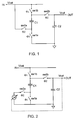
- FIG. 1 An example of a voltage multiplying circuit capable of delivering output currents of considerable size (up to a few tenths of a mA) as in the case of integrated analog circuits for which the power supply voltage must be doubled or tripled for operational reasons is shown in FIG. 1.
- the first capacitor C1 serves to take and transfer electric charges from the input terminal of the multiplier to the output terminal while the second capacitor C2 serves to store these charges.
- the four switches are piloted by means of a first phase signal ⁇ 1 and a second phase signal ⁇ 2 not temporally overlapped.
- a first phase ⁇ 1 the charge transfer capacitor C1 is connected between the power voltage Vbat and a ground and then on the upper plate there develops a voltage equal to Vbat in relation to the lower plate.
- the second phase ⁇ 2 the lower plate is placed at Vbat while the upper plate is connected to the output node on which develops a voltage Vout higher than the voltage Vbat.
- the value of the output voltage Vout would be influenced by the voltage drops on the capacitors and on the switches which depend on the current value, on the process used and on the working temperature.
- the boosted output voltage Vout be kept constant even with changes in the value of the supply voltage Vbat, e.g. in the case of battery-powered systems, because battery voltage can vary even greatly during discharge of same. In these cases it is necessary to stabilise output voltage Vout by means of a special regulation circuit.
- the voltage multiplier described in said patent application is the same type described above and the stabilization circuit is provided by means of a negative regulation loop for the output voltage Vout.
- the regulation loop is achieved by means of an integrator designed to generate a continuous error signal proportional to the difference between the output voltage of the voltage multiplier and a reference voltage.
- This error signal is used to pilot (in a conduction phase of the operation cycle of the voltage multiplying circuit) a transistor acting as a connection switch of the charge transfer capacitor at the power supply voltage controlling its internal resistance and hence the capacitor charge time constant. In this manner it is managed, with rated operation, to keep constant the value of the output voltage of the voltage multiplying circuit.
- a non-linear feedback loop can exhibit considerable "locking time” problems, i.e. reaching the correct output voltage from the moment when the circuit is started, and problems in holding said output voltage after current peaks due to sudden load absorption.
- the technical problem underlying the present invention is to conceive a voltage multiplier or booster for relatively high output currents having structural and functional characteristics allowing output voltage to be stable and virtually independent of the power supply voltage, temperature, the process and, within certain limits, also of the load absorbed current, thereby overcoming the shortcomings indicated above with reference to the known art.
- the lower plate of the capacitor C1 is connected during the phase ⁇ 2 of the control clock cycle to a variable voltage generator depending linearly on the value of the voltage Vout present on the output node OUT of the voltage multiplier.
- FIG.3 An analogous solution from the functional viewpoint is shown in FIG.3 where the lower plate of the capacitor C1 is connected during the phase ⁇ 1 of the control clock cycle to a variable voltage generator depending linearly on the value of the voltage Vout present on the output node OUT of the voltage multiplier.
- a voltage divider which in the example shown consists of the two resistances R1 and R2 when connected in series between the output node OUT of the voltage multiplying circuit and ground supplies an attenuated replica Vx of the output voltage Vout of the multiplying circuit at the inverting input of an operational amplifier OA which, being powered at Vbat could not otherwise support an input voltage higher than Vbat.
- the operational amplifier OA together with the capacitive feedback network RZ-CI constitutes the integrator stage.
- a transfer switch or gate which, in the example shown consists of the pair of MOS transistors M4 and M5 is controlled by the phase signal ⁇ 2 and by its complementary signal and transfers during the phase ⁇ 2 of the control clock cycle the error signal produced by the integrator stage directly on the lower plate of the charge transfer capacitor C1.
- the resistance RZ in series with the integration capacitor CI of the feedback line of the operational amplifier OA has a non-secondary function for the purpose of assuring great stability to the system. Indeed, in the stabilization loop there are two low-frequency poles which tend to severely reduce the margin of stability of the circuit.
- the introduction of a resistance RZ in series with CI causes the creation of a low-frequency zero which compensates for a pole and hence improves the stability of the system.
- a second circuitry solution derived from the circuit of FIG. 4 and shown in FIG. 5 permits decreasing the area occupied by the switching transistors. This solution is particularly suitable when the current absorbed by the load is high (>10mA).
- the integrator comprises an operational amplifier OA whose inverting input is connected to the central node of the voltage divider R1-R2 and through the series of the resistance RZ, the integration capacitor CI and a transfer switch or gate M7-M8 to the output of the amplifier.
- the non-inverting input is connected through a switch M9 to a reference voltage Vrif and by means of another switch M10 to a ground potential.
- the MOS transistors M7 and M8 are piloted by the phase signal ⁇ 2 and by its complementary signal, the transistor M9 is piloted by the phase signal ⁇ 2 and the transistor M10 is piloted by the phase signal ⁇ 1.
- the lower plate of the charge transfer capacitor C1 is forced to the ground potential of the operational amplifier OA since its feedback loop is open and its non-inverting input is connected to ground while the upper plate of the charge transfer capacitor C1 is connected to the power voltage Vbat. In this manner the charge transfer capacitor C1 is charged at the power voltage Vbat.
- the non-inverting input of the operational amplifier OA is brought to the reference voltage Vrif by means of closing of the transistor M9 and simultaneously the feedback loop of the operational amplifier OA is closed.
- the output voltage of the operational amplifier OA reaches a value proportionate to the integral of the error between the reference voltage Vrif and the output voltage Vout*(R1/(R1+R2)) .
- FIG. 6 shows the temporal diagrams of the control phases employed in the circuits of FIGS. 4 and 5 in accordance with two embodiments of the circuit of the present invention.
- phase ⁇ 1 ⁇ is virtually coincident with the phase ⁇ 1sur ⁇ while the phase ⁇ 2 ⁇ is essentially coincident with the phase ⁇ 2sur ⁇ .
- the phases ⁇ 1sur ⁇ and ⁇ 2sur ⁇ are commonly generated by a timing circuit powered with the. output voltage Vout.
- the pilot phases ⁇ 1sur ⁇ and ⁇ 2sur ⁇ are voltage boosted phases.
- circuit in accordance with the present invention allows provision of a voltage multiplier or booster for relatively high output currents whose output voltage is stable and virtually independent of the power supply voltage, temperature and, within certain limits, the current absorbed by the load.
- the initial settling time upon starting of the circuit is very short, i.e. on the order of 500 microseconds as compared with the tens of milliseconds typical of the circuits of the known art.
Landscapes
- Engineering & Computer Science (AREA)
- Power Engineering (AREA)
- Dc-Dc Converters (AREA)
- Semiconductor Integrated Circuits (AREA)
Priority Applications (4)
| Application Number | Priority Date | Filing Date | Title |
|---|---|---|---|
| EP94830413A EP0700146B1 (fr) | 1994-08-31 | 1994-08-31 | Multiplicateur de tension avec tension de sortie stabilisée lineairement |
| DE69424668T DE69424668T2 (de) | 1994-08-31 | 1994-08-31 | Spannungsvervielfacher mit linearstabilisierten Ausgangspannung |
| US08/414,277 US5712777A (en) | 1994-08-31 | 1995-03-31 | Voltage multiplier with linearly stabilized output voltage |
| JP7223518A JPH0898512A (ja) | 1994-08-31 | 1995-08-31 | 出力電圧安定化回路およびそれを用いた電圧増倍器 |
Applications Claiming Priority (1)
| Application Number | Priority Date | Filing Date | Title |
|---|---|---|---|
| EP94830413A EP0700146B1 (fr) | 1994-08-31 | 1994-08-31 | Multiplicateur de tension avec tension de sortie stabilisée lineairement |
Publications (2)
| Publication Number | Publication Date |
|---|---|
| EP0700146A1 true EP0700146A1 (fr) | 1996-03-06 |
| EP0700146B1 EP0700146B1 (fr) | 2000-05-24 |
Family
ID=8218515
Family Applications (1)
| Application Number | Title | Priority Date | Filing Date |
|---|---|---|---|
| EP94830413A Expired - Lifetime EP0700146B1 (fr) | 1994-08-31 | 1994-08-31 | Multiplicateur de tension avec tension de sortie stabilisée lineairement |
Country Status (4)
| Country | Link |
|---|---|
| US (1) | US5712777A (fr) |
| EP (1) | EP0700146B1 (fr) |
| JP (1) | JPH0898512A (fr) |
| DE (1) | DE69424668T2 (fr) |
Cited By (7)
| Publication number | Priority date | Publication date | Assignee | Title |
|---|---|---|---|---|
| WO1998045931A1 (fr) * | 1997-04-10 | 1998-10-15 | Telefonaktiebolaget Lm Ericsson (Publ) | Procede et systeme dans un transformateur cc/cc |
| DE19752985A1 (de) * | 1997-11-28 | 1999-06-02 | Siemens Ag | Halbleiterschaltungsanordnung mit monolithisch integrierten Schaltkreisen und einer Spannungspumpenschaltung |
| WO1999050862A1 (fr) * | 1998-03-30 | 1999-10-07 | Astrazeneca Ab | Circuit d'amplification de tension comprenant un condensateur a capacite parasite reduite |
| EP1202439A3 (fr) * | 2000-10-11 | 2002-11-06 | Texas Instruments Deutschland Gmbh | Convertisseur continu-continu |
| EP1271756A1 (fr) * | 2001-06-20 | 2003-01-02 | Alcatel | Circuit de pompe de charge |
| WO2002039568A3 (fr) * | 2000-10-11 | 2003-01-30 | Tropian Inc | Doubleur de tension |
| EP0952661A3 (fr) * | 1998-04-24 | 2003-08-27 | Infineon Technologies AG | Circuit pour une pompe de charge et régulateur de tension comportant un tel circuit |
Families Citing this family (18)
| Publication number | Priority date | Publication date | Assignee | Title |
|---|---|---|---|---|
| US6125047A (en) * | 1993-12-14 | 2000-09-26 | Seagate Technology, Inc. | Regulated inverting power supply |
| FI101914B (fi) * | 1996-11-08 | 1998-09-15 | Nokia Mobile Phones Ltd | Parannettu menetelmä ja piirijärjestely signaalin käsittelemiseksi |
| FR2778286B1 (fr) * | 1998-04-30 | 2002-04-12 | Sgs Thomson Microelectronics | Circuit convertisseur de tension |
| KR100275743B1 (ko) * | 1998-09-08 | 2001-01-15 | 윤종용 | 승압회로 및 그의 승압방법 |
| TW504887B (en) * | 1998-10-20 | 2002-10-01 | Hitachi Eng Co Ltd | Voltage booster circuit apparatus and control method therefor |
| US6778347B2 (en) | 2000-11-20 | 2004-08-17 | Seagate Technology Llc | Load balancing circuit for a dual polarity power supply with single polarity voltage regulation |
| KR100374644B1 (ko) * | 2001-01-27 | 2003-03-03 | 삼성전자주식회사 | 승압 전압의 조절이 가능한 전압 승압 회로 |
| DE10336090A1 (de) * | 2003-08-06 | 2005-03-10 | Infineon Technologies Ag | Ladungspumpenregelkreis |
| US20050075809A1 (en) * | 2003-09-18 | 2005-04-07 | Ewc Controls Incorporated | Apparatus and method for detecting, filtering and conditioning AC voltage signals |
| DE102004060969A1 (de) * | 2004-12-17 | 2006-07-13 | Infineon Technologies Ag | Integrierte Ladungspumpe |
| WO2010039046A2 (fr) * | 2008-10-01 | 2010-04-08 | Restech Limited | Circuit et procédé de couplage d'énergie électrique à une charge inductive à résonnance |
| CA2771935C (fr) * | 2009-08-25 | 2018-06-12 | Charles Francis Neugebauer | Pompe de charge regulee a haut rendement |
| JP5087670B2 (ja) * | 2010-11-01 | 2012-12-05 | 株式会社東芝 | 電圧発生回路 |
| US9438062B2 (en) * | 2012-10-12 | 2016-09-06 | Samsung Electronics Co., Ltd | Wireless electric power receiver for wirelessly regulating electric power using switch |
| CN103501111B (zh) * | 2013-10-08 | 2015-09-23 | 北京控制工程研究所 | 一种低噪声、高稳定度红外偏置电源 |
| CN107274920B (zh) * | 2016-04-08 | 2020-05-08 | 中芯国际集成电路制造(上海)有限公司 | 用于存储器的电压维持电路、存储器及电子设备 |
| US10790741B2 (en) | 2018-09-24 | 2020-09-29 | Psemi Corporation | Pole compensation in reconfigurable power converter |
| TWI713302B (zh) * | 2019-01-04 | 2020-12-11 | 周重甫 | 具功率回授之音頻放大器架構及方法 |
Citations (1)
| Publication number | Priority date | Publication date | Assignee | Title |
|---|---|---|---|---|
| EP0540948A2 (fr) * | 1991-11-07 | 1993-05-12 | Motorola, Inc. | Pompe de charge régulée et procédé de commande |
Family Cites Families (11)
| Publication number | Priority date | Publication date | Assignee | Title |
|---|---|---|---|---|
| US4636930A (en) * | 1985-10-01 | 1987-01-13 | Maxim Integrated Products, Inc. | Integrated dual charge pump power supply and RS-232 transmitter/receiver |
| US4807104A (en) * | 1988-04-15 | 1989-02-21 | Motorola, Inc. | Voltage multiplying and inverting charge pump |
| GB2245112A (en) * | 1990-06-13 | 1991-12-18 | Philips Electronic Associated | Dc/dc voltage multiplier. |
| US5051881A (en) * | 1990-07-05 | 1991-09-24 | Motorola, Inc. | Voltage multiplier |
| US5132895A (en) * | 1990-12-11 | 1992-07-21 | Motorola, Inc. | Variable charge pumping DC-to-DC converter |
| US5111375A (en) * | 1990-12-20 | 1992-05-05 | Texas Instruments Incorporated | Charge pump |
| JPH04222455A (ja) * | 1990-12-20 | 1992-08-12 | Nec Corp | インタフェース回路 |
| JPH05268763A (ja) * | 1992-03-17 | 1993-10-15 | Nec Corp | Dc/dcコンバータ回路およびそれを用いたrs−232インタフェース回路 |
| US5306954A (en) * | 1992-06-04 | 1994-04-26 | Sipex Corporation | Charge pump with symmetrical +V and -V outputs |
| US5262934A (en) * | 1992-06-23 | 1993-11-16 | Analogic Corporation | Bipolar voltage doubler circuit |
| US5493543A (en) * | 1994-11-07 | 1996-02-20 | Timex Corporation | Capacitive charge pump driver circuit for piezoelectric alarm |
-
1994
- 1994-08-31 DE DE69424668T patent/DE69424668T2/de not_active Expired - Fee Related
- 1994-08-31 EP EP94830413A patent/EP0700146B1/fr not_active Expired - Lifetime
-
1995
- 1995-03-31 US US08/414,277 patent/US5712777A/en not_active Expired - Lifetime
- 1995-08-31 JP JP7223518A patent/JPH0898512A/ja active Pending
Patent Citations (1)
| Publication number | Priority date | Publication date | Assignee | Title |
|---|---|---|---|---|
| EP0540948A2 (fr) * | 1991-11-07 | 1993-05-12 | Motorola, Inc. | Pompe de charge régulée et procédé de commande |
Cited By (10)
| Publication number | Priority date | Publication date | Assignee | Title |
|---|---|---|---|---|
| WO1998045931A1 (fr) * | 1997-04-10 | 1998-10-15 | Telefonaktiebolaget Lm Ericsson (Publ) | Procede et systeme dans un transformateur cc/cc |
| US5939866A (en) * | 1997-04-10 | 1999-08-17 | Telefonaktiebolaget L M Ericsson | Preregulated DC-to-DC converter |
| DE19752985A1 (de) * | 1997-11-28 | 1999-06-02 | Siemens Ag | Halbleiterschaltungsanordnung mit monolithisch integrierten Schaltkreisen und einer Spannungspumpenschaltung |
| WO1999050862A1 (fr) * | 1998-03-30 | 1999-10-07 | Astrazeneca Ab | Circuit d'amplification de tension comprenant un condensateur a capacite parasite reduite |
| EP0952661A3 (fr) * | 1998-04-24 | 2003-08-27 | Infineon Technologies AG | Circuit pour une pompe de charge et régulateur de tension comportant un tel circuit |
| EP1202439A3 (fr) * | 2000-10-11 | 2002-11-06 | Texas Instruments Deutschland Gmbh | Convertisseur continu-continu |
| WO2002039568A3 (fr) * | 2000-10-11 | 2003-01-30 | Tropian Inc | Doubleur de tension |
| US6522192B1 (en) | 2000-10-11 | 2003-02-18 | Tropian Inc. | Boost doubler circuit |
| EP1271756A1 (fr) * | 2001-06-20 | 2003-01-02 | Alcatel | Circuit de pompe de charge |
| US6717829B2 (en) | 2001-06-20 | 2004-04-06 | Alcatel | Charge pump device with reduced ripple and spurious low frequency electromagnetic signals |
Also Published As
| Publication number | Publication date |
|---|---|
| EP0700146B1 (fr) | 2000-05-24 |
| US5712777A (en) | 1998-01-27 |
| JPH0898512A (ja) | 1996-04-12 |
| DE69424668D1 (de) | 2000-06-29 |
| DE69424668T2 (de) | 2001-01-25 |
Similar Documents
| Publication | Publication Date | Title |
|---|---|---|
| EP0700146B1 (fr) | Multiplicateur de tension avec tension de sortie stabilisée lineairement | |
| US5754417A (en) | Linearly regulated voltage multiplier | |
| EP0631369A1 (fr) | Multiplicateur de tension avec courant de sortie elevé et tension de sortie stabilisée | |
| US6791306B2 (en) | Synthetic ripple regulator | |
| US4868908A (en) | Power supply down-conversion, regulation and low battery detection system | |
| US4952864A (en) | Power supply down-conversion, regulation and low battery detection system | |
| US7362083B2 (en) | DC-DC converter with modulator circuit having a feed forward structure | |
| US5247239A (en) | Dual dc/dc voltage converter power system | |
| US20080088179A1 (en) | Switching Power Supply And Electronic Apparatus Employing The Same | |
| US20060049815A1 (en) | Current feed-through adaptive voltage position control for a voltage regulator | |
| KR100561945B1 (ko) | 벅 부스트 스위칭 조정기 | |
| KR20060109977A (ko) | 세그먼트된 스위칭을 이용한 dc/dc 컨버터를 조정하기위한 디지털 루프 | |
| EP1655825A2 (fr) | Etalonnage du decalage de la tension pour un circuit amplificateur intégré | |
| TWI387189B (zh) | 直流對直流轉換器及其方法 | |
| EP0498553A2 (fr) | Méthode de commande adaptive pour des convertisseurs de puissance | |
| CN113114184A (zh) | 功率级和电流监视器输出信号产生电路 | |
| US12334811B2 (en) | Closed loop stability ramp implementation for Constant On-Time buck converter | |
| US5079453A (en) | Slope compensation circuit for stabilizing current mode converters | |
| JP2704518B2 (ja) | 電源回路 | |
| EP0793333A1 (fr) | Pompe à charge | |
| JP2018516524A (ja) | 改善されたトラッキング | |
| CN111010023B (zh) | 开关模式功率转换器 | |
| US7145381B2 (en) | Apparatus for controlling a boosted voltage and method of controlling a boosted voltage | |
| EP0766162A2 (fr) | Circuit pour améliorer la réponse aux transitoires de charges dans des alimentations | |
| US10985656B2 (en) | Systems and methods for providing intelligent constant on-time control |
Legal Events
| Date | Code | Title | Description |
|---|---|---|---|
| PUAI | Public reference made under article 153(3) epc to a published international application that has entered the european phase |
Free format text: ORIGINAL CODE: 0009012 |
|
| AK | Designated contracting states |
Kind code of ref document: A1 Designated state(s): DE FR GB IT |
|
| 17P | Request for examination filed |
Effective date: 19960828 |
|
| 17Q | First examination report despatched |
Effective date: 19970918 |
|
| RAP3 | Party data changed (applicant data changed or rights of an application transferred) |
Owner name: STMICROELECTRONICS S.R.L. |
|
| GRAG | Despatch of communication of intention to grant |
Free format text: ORIGINAL CODE: EPIDOS AGRA |
|
| GRAG | Despatch of communication of intention to grant |
Free format text: ORIGINAL CODE: EPIDOS AGRA |
|
| GRAH | Despatch of communication of intention to grant a patent |
Free format text: ORIGINAL CODE: EPIDOS IGRA |
|
| GRAH | Despatch of communication of intention to grant a patent |
Free format text: ORIGINAL CODE: EPIDOS IGRA |
|
| GRAA | (expected) grant |
Free format text: ORIGINAL CODE: 0009210 |
|
| AK | Designated contracting states |
Kind code of ref document: B1 Designated state(s): DE FR GB IT |
|
| ITF | It: translation for a ep patent filed | ||
| REF | Corresponds to: |
Ref document number: 69424668 Country of ref document: DE Date of ref document: 20000629 |
|
| ET | Fr: translation filed | ||
| PLBE | No opposition filed within time limit |
Free format text: ORIGINAL CODE: 0009261 |
|
| STAA | Information on the status of an ep patent application or granted ep patent |
Free format text: STATUS: NO OPPOSITION FILED WITHIN TIME LIMIT |
|
| 26N | No opposition filed | ||
| REG | Reference to a national code |
Ref country code: GB Ref legal event code: IF02 |
|
| PGFP | Annual fee paid to national office [announced via postgrant information from national office to epo] |
Ref country code: DE Payment date: 20030808 Year of fee payment: 10 |
|
| PG25 | Lapsed in a contracting state [announced via postgrant information from national office to epo] |
Ref country code: DE Free format text: LAPSE BECAUSE OF NON-PAYMENT OF DUE FEES Effective date: 20050301 |
|
| PG25 | Lapsed in a contracting state [announced via postgrant information from national office to epo] |
Ref country code: IT Free format text: LAPSE BECAUSE OF NON-PAYMENT OF DUE FEES;WARNING: LAPSES OF ITALIAN PATENTS WITH EFFECTIVE DATE BEFORE 2007 MAY HAVE OCCURRED AT ANY TIME BEFORE 2007. THE CORRECT EFFECTIVE DATE MAY BE DIFFERENT FROM THE ONE RECORDED. Effective date: 20050831 |
|
| PGFP | Annual fee paid to national office [announced via postgrant information from national office to epo] |
Ref country code: FR Payment date: 20130820 Year of fee payment: 20 Ref country code: GB Payment date: 20130725 Year of fee payment: 20 |
|
| REG | Reference to a national code |
Ref country code: GB Ref legal event code: PE20 Expiry date: 20140830 |
|
| PG25 | Lapsed in a contracting state [announced via postgrant information from national office to epo] |
Ref country code: GB Free format text: LAPSE BECAUSE OF EXPIRATION OF PROTECTION Effective date: 20140830 |