EP0700187A2 - Verfahren und Vorrichtung zum Vermittlen von Zellen - Google Patents
Verfahren und Vorrichtung zum Vermittlen von Zellen Download PDFInfo
- Publication number
- EP0700187A2 EP0700187A2 EP19950113382 EP95113382A EP0700187A2 EP 0700187 A2 EP0700187 A2 EP 0700187A2 EP 19950113382 EP19950113382 EP 19950113382 EP 95113382 A EP95113382 A EP 95113382A EP 0700187 A2 EP0700187 A2 EP 0700187A2
- Authority
- EP
- European Patent Office
- Prior art keywords
- cell
- buffer
- access
- read
- switching apparatus
- Prior art date
- Legal status (The legal status is an assumption and is not a legal conclusion. Google has not performed a legal analysis and makes no representation as to the accuracy of the status listed.)
- Granted
Links
Images
















Classifications
-
- H—ELECTRICITY
- H04—ELECTRIC COMMUNICATION TECHNIQUE
- H04L—TRANSMISSION OF DIGITAL INFORMATION, e.g. TELEGRAPHIC COMMUNICATION
- H04L12/00—Data switching networks
- H04L12/54—Store-and-forward switching systems
- H04L12/56—Packet switching systems
- H04L12/5601—Transfer mode dependent, e.g. ATM
-
- H—ELECTRICITY
- H04—ELECTRIC COMMUNICATION TECHNIQUE
- H04L—TRANSMISSION OF DIGITAL INFORMATION, e.g. TELEGRAPHIC COMMUNICATION
- H04L49/00—Packet switching elements
- H04L49/10—Packet switching elements characterised by the switching fabric construction
- H04L49/104—Asynchronous transfer mode [ATM] switching fabrics
- H04L49/105—ATM switching elements
- H04L49/106—ATM switching elements using space switching, e.g. crossbar or matrix
-
- H—ELECTRICITY
- H04—ELECTRIC COMMUNICATION TECHNIQUE
- H04L—TRANSMISSION OF DIGITAL INFORMATION, e.g. TELEGRAPHIC COMMUNICATION
- H04L49/00—Packet switching elements
- H04L49/10—Packet switching elements characterised by the switching fabric construction
- H04L49/104—Asynchronous transfer mode [ATM] switching fabrics
- H04L49/105—ATM switching elements
- H04L49/108—ATM switching elements using shared central buffer
-
- H—ELECTRICITY
- H04—ELECTRIC COMMUNICATION TECHNIQUE
- H04L—TRANSMISSION OF DIGITAL INFORMATION, e.g. TELEGRAPHIC COMMUNICATION
- H04L12/00—Data switching networks
- H04L12/54—Store-and-forward switching systems
- H04L12/56—Packet switching systems
- H04L12/5601—Transfer mode dependent, e.g. ATM
- H04L2012/5678—Traffic aspects, e.g. arbitration, load balancing, smoothing, buffer management
- H04L2012/5679—Arbitration or scheduling
-
- H—ELECTRICITY
- H04—ELECTRIC COMMUNICATION TECHNIQUE
- H04L—TRANSMISSION OF DIGITAL INFORMATION, e.g. TELEGRAPHIC COMMUNICATION
- H04L12/00—Data switching networks
- H04L12/54—Store-and-forward switching systems
- H04L12/56—Packet switching systems
- H04L12/5601—Transfer mode dependent, e.g. ATM
- H04L2012/5678—Traffic aspects, e.g. arbitration, load balancing, smoothing, buffer management
- H04L2012/5681—Buffer or queue management
Definitions
- This invention relates to a cell switching apparatus or cell switching system which switches a cell, in which various types of multi media information such as speech, data, image and so forth are transmitted, at a high speed.
- ATM Asynchronous Transfer Mode
- consecutive signals such as a communication line signal and speech, and bursty signal such as data and motion video are all divided into a fixed length of signal.
- a header to indicate the destination information is then added to the fixed length of signal and thus a packet is composed.
- the information is transferred in the packet.
- a synchronization with a terminal and a network like a frame synchronization is not required and a speed at the terminal and the network is independent. Therefore, it is possible to handle ATM communications with any types of terminals.
- packets arrive randomly at the high speed packet switch, a large number of packets may rush to one destination at a time. As a result, queueing of packets would be advantageous in order to prevent the loss of the information.
- This article relates to the high speed packet switch in the ATM communication system which effectively multiplexes and transmits line switching data and packet switching data.
- a conventional data queue unit is included in a controller 160.
- Fig. 29 is a block diagram showing the example.
- a packet multiplexing circuit 130 multiplexes the input packets.
- a shared buffer memory 140 can write the data in the indicated address and read out data with an indicated address without relating to the writing order by indicating the address.
- a packet demultiplexing circuit 150 demultiplexes read out packets.
- the controller 160 controls the packet switching.
- memory operation speed is lower than gate operation speed. In this example, however, when the switch scale becomes large or the accommodated line speed becomes higher, the memory needs to operate faster.
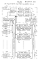
- Fig. 30 is a block diagram showing a conventional cell switching apparatus shown in Japanese Published and Unexamined Patent Hei 4-211548.
- a cell is composed of a header and a payload part.
- the header includes its channel or path number as the destination information.
- Header processing circuits 10a1 to 10a n are provided to each of the incoming lines 11 to 1 n .
- the header processing circuits 10a1 to 10a n detect the outgoing lines 21 to 2 m as its destination according to the header of a cell arriving at the incoming lines 11 to 1 n .
- the stored cell can be read out from the buffer memories 111 to 11 p with an indicated address without relating to the writing order.
- a plurality of cells can be stored in the whole buffer memories 111 to 11 p .
- Memory controllers 121 to 12 p are provided to each of the buffer memories 111 to 11 p .
- the memory controllers 121 to 12 p pool empty addresses by using the FIFO-type memory, for instance, and give the read addresses or write addresses to the corresponding buffer memories 111 to 11 p .
- An incoming line space switch 13 selectively connects the header processing circuits 10a1 to 10a n to appropriate buffer memories 111 to 11 p .
- An outgoing line space switch 14 selectively connects the buffer memories 111 to 11 p to appropriate outgoing lines 21 to 2 m .
- Outgoing line speed adjustment buffers 231 to 23 m are provided to each of the outgoing lines 21 to 2 m .
- the outgoing line speed adjustment buffers 231 to 23 m transmit the read out cells to the corresponding outgoing lines 21 to 2 m .
- a buffer controller 15 has a writing buffer selective circuit 16, an address switching circuit 17, address queues 181 to 18 m and a read out buffer selective circuit 19.
- the buffer controller 15 controls the switching of the incoming line space switch 13 and selects buffers 111 to 11 p in which the cell is written.
- the outgoing line space switch 14 is controlled in order that the cells are transmitted to the outgoing lines 21 to 2 m indicated in their headers.
- the cells are then written in the associated outgoing line speed adjustment buffers 231 to 23 m .
- the cells are next read out at the outgoing-line speed to be transmitted to the associated outgoing lines 21 to 2 m .
- the writing buffer selective circuit 16 receives the outgoing line number of the cell detected by the header processing circuits 10a1 to 10a n associated with the incoming lines 11 to 1 n . In order to select buffer memories 111 to 11 p for storing the cell and to connect the selected buffer memory to the header processing circuits 10a1 to 10a n , the writing buffer selective circuit 16 controls the switching of the incoming line space switch 13.
- An address switching circuit 17 sorts the arriving cells with reference to the outgoing line numbers detected by the buffer selective circuit 16.
- the write addresses in the buffer memories 111 to 11 p in which the cells are written are received from the memory controllers 121 to 12 p associated with the buffer memories 111 to 11 p . Then, the write addresses are written into address queues which will be mentioned later.
- the address queues 181 to 18 m are composed of the FIFO type memories and provided corresponding to each outgoing line 21 to 2 m .
- the write address on the buffer memories 111 to 11 p is written by the address switching circuit 17 in the arriving order.
- the buffer memories 111 to 11 p the cells whose destinations are the outgoing lines 21 to 2 n are stored.
- the read out buffer selective circuit 19 chooses the cell to be read out from the buffer memories 111 to 11 p with reference to the address queues 181 to 18 m .
- the read out buffer selective circuit 19 reads out the addresses from the address queues 181 to 18 m , and sends them to the memory controllers 121 to 12 p which are associated with the buffer memories 111 to 11 p .
- the read out buffer selective circuit 19 controls the switching of the outgoing line space switch 14 which connects the buffer memories 111 to 11 p to the associated outgoing lines 21 to 2 m .
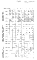
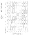
- Figs. 31 to 33 are timing charts showing an example of each element.
- the chart shows a flow of control in a case where the number of incoming lines 11 to 1 n , n is four and the number of outgoing lines 21 to 2 m , is four as well and the number of buffer memories 111 to 11 p , p is 10.
- the cell handled here has a fixed length and comes randomly. Before arriving at the incoming lines 11 to 1 n , cell input phase is adjusted, namely the cells arriving at all the lines have the same phase.
- FIGs. 31-33 show one example of the cell input to the incoming lines 11 to 14.
- (E) to (N) show one example of the stored cells in the buffer memories 111 to 1110.
- (O) to (R) show one example of cells to be transmitted from the outgoing lines 21 to 24.
- all the circuits are synchronized and the input and output of one cell can be done in one time slot.
- the header processing circuits 10a1 to 10a4 which are associated with each incoming lines 11 to 14 detect the outgoing line number from the headers of the incoming cells.
- the writing buffer selective circuit 16 in the buffer controller 15 directs the incoming line space switch 13 to connect the incoming lines 11 to 14 where the cell arrived to the buffer memories 111 to 1110 which are selected to store the cells, respectively, with reference to the header processing circuits 10a1 to 10a4.
- the number of the buffer memories is insufficient when it equals to the number of the incoming lines 11 to 14.
- having as many buffer memories as possible can simplify the control.
- buffer memories 111 to 1110 are selected in order, and the arriving cells are being written. Namely, the buffer memories 111, 112, 113, ⁇ 1110 are selected in regular order and the arriving cells are being written.
- F1 cell the first cell of a signal f (Hereinafter, the first cell of the signal f is referred to as F1 cell. Other cells which will be described are referred to in the same way.), is received from the incoming line 11.
- G1 cell of a signal g is received from the incoming line 12 and an I1 cell of a signal i is input from the incoming line 14.
- the header part of each cell has an outgoing line number of the destination. i.e., F1 cell has O1 to indicate the outgoing line 21, G1 cell has O4 to indicate the outgoing line 24 and I1 cell ha O3 to indicate the outgoinh line 23.
- the incoming line space switch 13 connects the incoming line 11 to the buffer memory 111, the incoming line 12 to the buffer memory 112, and the incoming line 14 to the buffer memory 113, respectively. Accordingly, in the time slot 2, these cells are stored at the address indicated by the memory controllers 121 to 123 in the buffer memories 111 to 113.
- the write address of each of the buffer memories 111 to 113 are transmitted to the address switching circuit 17.
- the write address is selected among the addresses which the memory controllers 121 to 123 manage as empty addresses.
- the address switching circuit 17 sorts each incoming cell according to the destination output lines with reference to the writing buffer selective circuit 16. The address switching circuit 17 then writes the write address of the buffer memory 111 on the address queue 181, the write address of the buffer memory 112 on the address queue 184 and the write address of the buffer memory 113 at the tail of the address queue 183, respectively.
- the read out buffer selective circuit 19 extracts the address stored in the address queues 181 to 184 and sends it to the memory controllers 121 to 123 associated with the buffer memories 111 to 113. Meanwhile, the read out buffer selective circuit 19 directs the outgoing space switch 14 to connect the buffer memories 111 to 113 to the outgoing lines 21, 23 and 24, respectively.
- the outgoing space switch 14 connects the buffer memory 111 to the outgoing line 21, the buffer memory 112 to the outgoing line 24, the buffer memory 113 to the outgoing line 23, respectively.
- Each of the memory controllers 121 to 123 transmits the received address to the associated buffer memories 11 to 113 as the read address. After that, the address is managed as an empty address.
- the cell read out from each of the buffer memories 111 to 113 are output to the destinations indicated by each header, i.e., the outgoing lines 21, 24, and 23.
- the destination outgoing lines of the input cell were all different.
- the cells input in the time slot 2 however have the identical destination outgoing line.
- An F2 cell, a G2 cell and an H1 cell input in the time slot 2 are written on the buffer memories 114, 115, and 116, respectively.
- Each of the headers of these three cells has O4 to indicate the outgoing line 24.
- the output priority of the outgoing cells is given in numerical order of the incoming line number and the queuing of the cell is carried out according to the priority.
- time slots 4, 5, and 6 the F2, the G2, and the H1 cells are read out in the order of the buffer memories 114, 115, 116 and transferred to the outgoing lines 34 based on the output priority.
- the switching of the cell is executed according to this procedure.
- an I2 cell and an H6 cell are stored in the buffer memory 113.
- each destination is different from each other.
- the destination is the outgoing line 22 and in case of the H6 cell, the outgoing line 23. If they are read out at the same speed of the outgoing line speed of the outgoing lines 21 to 24, they cannot be extracted simultaneously because both of them are stored in a single buffer memory, i.e. , the buffer memory 113.
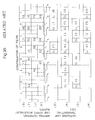
- Figs. 34 to 35 are timing charts showing extended parts of time slots 6 to 13 in Figs. 31 to 33.
- Figs. 34 to 35 there is shown a case that the read out of the buffer memories 111 to 1110 is performed at a three times of outgoing line speed.
- (E) to (N) show an example of stored cells
- (S) to (V) show a writing state of the cell to the outgoing line speed adjustment buffers 231 to 234.
- (O) to (R) show an example of cell output from the outgoing lines 21 to 24.
- each of the I2 cell and the H6 cell in the buffer memory 113 has its own destination.
- up to three cells can be read out from each of the buffer memories 111 to 1110 in the same time slot.
- the read out speed of the buffer memories 111 to 1110 is assumed to be three times of the outgoing line speed.
- the read out speed can be r times of the outgoing line speed, which is more than two times and less than the number of outgoing lines.
- a dual-port memory can be used as each of the buffer memories 111 to 1110.
- a single-port memory operable at more than a double speed is also useful.
- the number of cells to be read out from the same buffer memory, in one time slot exceeds the number r, it is possible to avoid all the collision when only the r number of cells are extracted by giving the priority corresponding to the outgoing lines 21 to 2 m .
- the priority should be updated at each time according to a predefined method or randomly. In this way, waiting of cells is not happening even though the plurality of cells are in the same queue and the output cell collision can be prevented.
- Fig. 36 is a block diagram showing a configuration of a conventional cell switching apparatus. The same signs are attached to the elements equivalent or corresponding to those of the cell switching apparatus according to the related art 2 and the explanation will be omitted.
- incoming-line speed-adjustment buffers 241 to 24 n are provided associated with each of the incoming lines 11 to 1 n .
- the cell transmitted from the associated header processing circuits 10a1 to 10a n is stored in incoming-line speed-adjustment buffers 241 to 24 n .
- the buffer controller 15 has the writing buffer selective circuit 16, the address switching circuit 17, the address queues 181 to 18 m , and the read out buffer selective circuit 19.
- the buffer controller 15 controls the outgoing line space switch 14 and transmits the cell to the outgoing lines 21 to 2 m indicated at the header of the cell in an appropriate order.
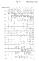
- Figs. 37 to 38 are timing charts showing the timing point of the signals of each element.
- the number of incoming lines 11 to 1 n , n and the number of outgoing lines 21 to 2 m , m are four, respectively and the number of the buffer memories 111 to 11 p , p is ten.
- the (A) to (R) are equivalent to those in Figs. 31 to 33, respectively.
- each of the buffer memories 111 to 11 p is two cells.
- the cell treated here arrives at random in a fixed length. Before coming to the incoming lines 11 to 1 n , the cell input phase is adjusted and the cell arriving at all the lines is assumed to be supplied with the same phase.
- the header processing circuits 101 to 104 associated with each of the incoming lines 11 to 14 detect the outgoing line number from the header and writes the cell in the associated incoming-line speed-adjustment buffers 241 to 244.
- the writing buffer selective circuit 16 in the buffer controller 15 directs the incoming line space switch 13 to connect the incoming line speed adjustment buffers 241 to 244 with the buffer memories 111 to 1110 selected to store the cell.
- the read out speed of the incoming-line speed-adjustment buffers 241 to 244, i.e., the writing speed of the buffer memories 111 to 1110 are assumed to be twice of the incoming line speed of the incoming lines 11 to 14. In one time slot, two cells can be written in the same buffer memory.
- buffer memories 111, 112, 113, etc10 are selected in this order and the arrived cells are being consecutively written.
- the buffer memory is ignored and the cell is written in the next buffer memory.
- the write speed of the buffer memories 111 to 1110 is set to be twice of the incoming speed. Accordingly, in a case where there occurs a cell discard in one buffer memories 111 to 1110, the writing of plural cells (two cells) in one time slot is allowed so as to lower the chance of cell discard.
- the cell discard is prevented by writing two cells, the F10 cell and the H10 cell in the buffer memory 116. There is shown a state that the writing of these three cells is finished in (J), (K) of Fig. 38 surrounded by the actual line.
- the write speed to the buffer memories 111 to 1110 is assumed to be twice of the incoming line speed.
- the incoming line speed can be w times. W is more than two and less than the number of incoming lines.
- a dual-port memory can be used.
- a single-port memory operable more than a double speed is also useful.
- the SBM shared buffer memory
- This invention solves the foregoing problems to provide the cell switching apparatus which increases the number of incoming lines and the number of outgoing lines without increasing the access speed of the buffer memory.
- the cell switching apparatus By using the cell switching apparatus, it is an object of this invention to provide the cell switching system which has a large scale of switch and can change the scale of the switch based on a building block basis according to the applicating system.
- a cell switching apparatus may include: a plurality of incoming lines for receiving a cell having data and a header that includes destination information; a plurality of outgoing lines, the cell being transmitted from a selected outgoing line of the plurality of outgoing lines according to the destination indicated by the header, during a predefined one cell time; a plurality of header processing circuits, connected to each of the incoming lines, for selecting the selected outgoing line according to the destination information from the header of the cell input from the incoming line; a plurality of buffer memories, the cell being written to a selected buffer memory of the plurality of buffer memories by indicating an address, and which is possible to read out the cell, without relating to a writing order of any other cells stored in the selected buffer memory, by indicating the address; an incoming line space switch for selectively connecting the header processing circuits to the buffer memories; an outgoing line space switch for selectively connecting the buffer memories to the outgoing lines; and, a buffer controller for controlling the incoming line space switch and selecting the selected buffer memory
- a cell switching system may include: a plurality of cell switching apparatuses, arranged in parallel, and a plurality of input lines respectively connected to the incoming lines of each of the plurality of cell switching apparatuses.
- a cell switching method for a cell switching apparatus may receive and transmit cells during a predefined one cell time, divide the predetermined cell time into a plurality of access intervals, and may read out and write one cell during one of the plurality of access intervals, the method may include the steps of:
- a method for performing a plurality of read accesses and a plurality of write accesses to a plurality of buffer memories during a predefined cell time so that a read access to one buffer memory of the plurality of buffer memories does not occur simultaneously with a write access to the one buffer memory may include the steps of: dividing the predefined cell time into a plurality of access times so that each of the plurality of buffer memories may be accessed during each of the plurality of access times; performing one first read access to one of the plurality of buffer memories and at least one write access to at least one other of the plurality of buffer memories during a first access time of the plurality of access times; performing one second read access to one of the plurality of buffer memories during a second access time of the plurality of access times; and when any of the plurality of write accesses remain after the first access time, performing at least one of the remaining write accesses to at least one other of the plurality of buffer memories during the second access time.
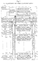
- Fig. 1 shows a view of one embodiment of a cell switching apparatus related to this invention.
- the identical signs are attached to the elements equivalent or corresponding to those of the cell switching apparatus according to the related arts and the explanation will be omitted.
- outgoing-line speed-adjustment buffers 231 to 23 m are provided to each outgoing line.
- the outgoing-line speed-adjustment buffers 231 to 23 m are connected to appropriate buffer memories according to an outgoing line space switch 14.
- the outgoing-line speed-adjustment buffers 231 to 23 m store the cell read out at a speed of more than r times (more than twice) of outgoing line speed from the buffer memory.
- the outgoing line speed adjustment buffers 231 to 23 m transmits the stored cell to the associated outgoing line according to the outgoing line speed.
- the incoming-line speed-adjustment buffers 241 to 24 n are provided to each incoming line.
- the incoming-line speed-adjustment buffers 241 to 24 n store the cell output from the associated header processing circuit.
- the incoming-line speed-adjustment buffers 241 to 24 n read out the stored cell at w times (twice, for example) of the incoming line speed and transfers the cell to an appropriate buffer connected by the incoming line space switch 13.
- An access controller 100 has a writing buffer selective circuit 16, a read-out-buffer selective circuit 19, and a schedule controller 101.
- the access controller 100 controls the writing buffer selective circuit 16 and the read out buffer selective circuit 19 by using the scheduling controller 101.
- Fig. 2 is a block diagram illustrating one embodiment of the schedule controller 101.
- the schedule controller has a scheduler 102 and a score table 103.
- the schedule controller 101 receives the information of the writing buffer to write the cell coming from the writing buffer selective circuit 16 (hereinafter, items in such information are referred to as, W1, W2, W3, (2003)).
- the schedule controller 101 receives the information of the read out buffer to read out the cell coming from the read-out-buffer selective circuit 19 (hereinafter, items in such information are referred to as, R1, R2, R3, .).
- the scheduler 102 makes a schedule based on these input information of the writing buffer and the read out buffer using the score table 103.
- the schedule controller 101 informs the writing buffer selective circuit 16 of the buffer to which the cell is to be written.
- the schedule controller 101 informs the read out buffer selective circuit 19 of the buffer to read out the cell.
- Fig. 3 is a view of one example of the score table 103.
- p the number of buffer memories
- the score table 103 is configured according to a matrix of (the number of buffer memories p) X (the number of divisions in one-cell time x). Namely, the score table 103 is composed of a field of p columns and m rows.
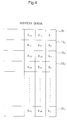
- Fig. 4 shows one example of address queues 181 to 18 m .
- the number of outgoing lines is eight.
- the information on each head of the address queues is the address information to read out the cell to be transmitted to each of the outgoing lines.
- the schedule controller 101 allocates the information R1 to R8 in order in each row, as shown in Fig. 3.
- R1 is the address of the cell to be transmitted to the outgoing line 21 and the address is contained in the memory buffer 4, for instance, as shown in the first row of Fig.
- R1 is allocated on the fourth column of the first row.
- R2 is the address information of the cell to be transmitted to the outgoing line 22.
- R2 is allocated on the fifth column of the second row.
- the information items R3 to R8 are allocated to each row of each column.
- the schedule controller 101 performs the scheduling to write the arriving cell. For example, as shown in Fig. 3, the schedule controller 101 schedules the writing information in the field except for the one where either of the R1 to R8 has been already allocated. In Fig. 3, it is possible to allocate the writing information W1 to W32. Fig. 3 does not imply that the 32 writings of the information, from the W1 to the W32, are always scheduled but that the writings here can be scheduled up to 32 at its maximum, for this example. Thus, the scheduler 102 schedules the access in order that the writing and the read out should not be overlapped.
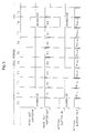
- Fig. 5 is a timing chart of a signal input or output to the schedule controller 101.
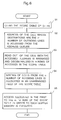
- Fig. 6 is a flow-chart showing the operation of a scheduler 102.
- the schedule controller 101 receives the information of the read out buffer (R1, R2, R3%) and the writing buffer (W1, W2, W3%) from the writing buffer selective circuit 16 and the read-out-buffer selective circuit 19, respectively.
- This input is performed at the final stage of each of the one-cell time.
- the input is performed at an interval of T0.
- the schedular performs scheduling based on the flow-chart as shown in Fig. 6.
- the value of each field of the score table shown in p columns and m rows is initialized with zero or space.
- the address information R1 to R8 of the cell for the m number of outgoing lines derived from the address queues is obtained.
- the obtained address information R1 to R8 are distributed and arranged in order in each row in the score table.
- the writing information of the cell coming to the writing buffer selective circuit 16 (W1, W2, W3 ...) is allocated on the unarranged field of the score table.
- the allocated accesses in the first to the m th row of the score table for each buffer memory are launched orderly row by row at each access interval to the writing buffer selective circuit 16 and the read-out-buffer selective circuit 19.
- the operation at S5 is executed in access intervals T1 to T8 as shown in Fig. 5.
- the information R1 to R8 is sent in order in each interval of T1 to T8.
- the writing-buffer selective circuit 16 in each interval of T1 to T8, the writing information W1 to W32 is transmitted at each row in order.
- the access interval of T1 as shown in Fig. 3, the writing of the cell is performed for the buffer memories #1 to #3 and #5.
- the read out of the cell is performed for the buffer memory #4.
- one-cell time is divided into a plurality of access intervals and the access is performed simultaneously for a plurality of buffer memories in one access interval.
- the schedular 102 performs the scheduling by using the score board 103 in order that the read out and writing should not be overlapped for a single buffer memory.
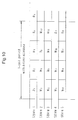
- Fig. 7 shows a general form of the score table 103 as shown in Fig. 3.
- the cell switching apparatus can perform the cell switching wherein the maximum number of incoming lines is 32 and the number of outgoing lines is 8. Namely, the number of incoming lines is excessively high, compared with the number of outgoing lines. Therefore, the schedule controller 101 performs the scheduling of the read out and writing of the cell by using the score table 103 and it is thus possible to realize the cell switching unit in a case where the number of incoming lines is excessively large compared with the conventional cell switching apparatus. By combining a plurality of cell switching apparatus as a whole unit, it comes to be able to configure a large scale cell switching system. Such a cell switching system will be described later.
- the R1 to R8 need to correspond to the outgoing lines.
- the scheduler 102 therefore reads out only one cell at its maximum for a single outgoing line in one-cell time.
- the W1 and W2 shown in Fig. 7 are the writing information of the cell coming from the incoming line 11 and the incoming line 12, and it may be indicated that the cells should be stored in the buffer memory 111 according to the writing buffer selective circuit 16.
- the W1 and W2 may be allocated not on the same row but on the different rows.
- the scheduler 102 thus detects the contents of the writing information of the cell and allocates the information on the score table 103.
- Fig. 8 shows one example when all of the fields of the score table 103 are not filled. There is shown that the access is not performed to some buffer memories in some access intervals. Fig. 8 shows a case where all the arrived cells to the incoming lines cannot be written on either of the buffer memories. When the arriving cell can not be written in any of the buffer memory, the cell is discarded.
- Fig. 9 shows a case where the one-cell time is divided by the larger number than the number of outgoing lines.
- the one-cell time is divided into (m + 2).
- Two access intervals on the left are assumed to be the intervals dedicated to the writing operations.
- M number of the other access intervals are assumed to be the intervals dedicated to the read-out operations.
- the scheduler 102 allocates the information W1 to W n to write the cells in advance from the writing-buffer selective circuit 16 on the intervals dedicated to the writing operations.
- the information R1 to R m to read out the cells from a read-out-buffer selective circuit 19 are allocated on the other intervals dedicated to the read out operations.
- the writing and read out of the cells is guaranteed.
- the minimum number of the intervals dedicated to the writing is only the quotient of (n + p) (when it is not divisible, the quotient of (n + p) + 1).
- the writing-buffer selective circuit 16 selects the buffer memory cyclicly in order, the buffer memory to write the cell is surely selected in order. Therefore, as shown in Fig. 9, the W1 to W n are arranged in order.
- the (n + p) + 1 number of access intervals are provided. As shown in Fig.
- the cells are not necessarily output for all the outgoing lines.
- more than five cells are read out from a single buffer memory, for instance, four access intervals are not sufficient. Consequently, the read out of the cell should be waited for the next cell time.
- Fig. 10 there is shown a case where the read out operations of the R1 to R5 occur for one buffer memory.
- the R1 to R4 can be allocated to each access interval and the R5 is allocated to the next cell time.
- the read out of the cell for all the outgoing lines is not guaranteed for one-cell time, it is possible to perform the effective access for more than two buffer memories in the single access interval by performing the access of the read out or writing.
- the buffer memory preferably offers the access speed which can perform the read out or writing of the cell in each access interval into which one-cell time is divided. Accordingly, it is possible to obtain the cell switching apparatus which increases the number of incoming lines without increasing the access speed of the buffer memory.
- the number of incoming lines can be increased not only because one-cell time is divided into a plurality of access intervals but also because the scheduling is performed so as to access to a plurality of buffer memories in one access interval.
- time for transmitting one cell is divided into a plurality of access intervals and the access operations such as the read out or writing are simultaneously performed.
- step S10 is added between S3 and S4 of the flow-chart as shown in Fig. 6.
- step S10 the contents of the score table in which the read out of the cell is already allocated at S3, is transmitted to the writing-buffer selective circuit 16.
- Fig. 12 is a flow-chart showing the operation of the writing-buffer selective circuit 16 to which the contents of the score table is transmitted.
- S11 with reference to the received contents of the score table, unarranged fields of the score table are detected.
- the buffer memory in which the arriving cell is written is determined for the detected unarranged fields.
- the determined buffer memory is transferred to the schedule controller 101.
- the schedule controller 101 executes the processes at S4 and S5 as shown in Fig. 11.
- the buffer memory is selected in advance in the writing-buffer selective circuit 16 so as to correspond to the unarranged field. Accordingly, the process of allocating the writing of the cell dose not overlap the operations of read out R1 to R m .
- the writing-buffer selective circuit 16 refers to empty fields of the score table and arranges the writing buffer memory of the arriving cell. It is therefore possible that the score table can be filled efficiently with the read out and writing operations.
- Fig. 13 shows a conceptional view of another embodiment of the cell switching apparatus related to this invention.
- the buffer memory has a plurality of ports. Specifically in Fig. 13, the buffer memory has a write port and a read port.
- the buffer memory in Fig. 1 is a single port memory. If the buffer memory has the single port, when the buffer memory performs writing, the read out cannot be performed. When the buffer memory performs the read out, the writing can not be performed. Accordingly, the scheduler 102 exclusively controlled a single buffer memory by using the score table 103 in order that the read out and writing should not overlap. However, as shown in Fig. 13, when the buffer memory has two ports, the read out and writing can be simultaneously performed.
- Figs. 14A and 14B show an example of the score tables when the buffer memory shown in Fig. 13 is utilized.
- a reading score table 13a and a writing score table 13b are provided.
- the reading score table information R1 to R m to read out the cell from the buffer memory are arranged orderly in each row. The fields except for the ones in which the R1 to R m are allocated remain empty.
- the writing score table 13b schedules the writing information coming from the writing-buffer selective circuit 16. Since the writing score table is dedicated to the writing, unlike the preceding Embodiment 1, the R1 to R m are not allocated in advance. Therefore, the scheduler 102 can allocate the writing information of the cell at the optional position for the writing score table 13b.
- the maximum number is (p x m).
- the write port shown in Fig. 13 writes the arriving cells in the buffer memory according to the schedule of the writing score table as shown in Fig. 14B.
- the read port performs the read out of the cell according to the schedule of the reading score table 13a shown in Fig. 14A.
- the access can be performed in parallel because the write port and the read port can operate independently.
- the writing from the write port and the read out from the read port do not come to be the same address. Because the read out is performed from the address in which the cell is recorded in advance, whereas the writing is performed for the address in which the cell is not written yet. The management of these addresses is performed according to the memory controllers 121 to 12 p and the buffer controller 15.
- Fig. 15 shows a view in a case where the buffer memory according to the embodiment has a plurality of ports.
- the buffer memory 11a has a write port and a read/write port. Accordingly, for the buffer memory 11a, it is possible to write two cells simultaneously by using both of the write port and the read/write port.
- the buffer memory 11b has a read/write port and a read port. Therefore, it is possible to read out two cells simultaneously from the buffer memory 11b by using the read/write port and the read port.
- the buffer memory 11c has two read/write ports. Then, for the buffer memory 11c, the simultaneous writing or read out of the two cells can be implemented. Thus, by providing a plurality of input and output ports for the buffer memory, it is possible to read out and write a plurality of cells without increasing the access speed of the buffer memory.
- a score table shown in Fig. 16A is available. That is, as a score table for the buffer memory 11a, a read/write score table as shown in Embodiment 1 and the writing score table as shown in Fig. 14B are utilized.
- the read/write score table corresponds to the read/write ports, while the writing score table corresponds to the write port.
- the read/write score table and the read score table are used for the buffer memory 11b.
- the read/write score table corresponds to the read write ports of the buffer memory llb and the read score table corresponds to the read port.
- read/write score table is provided for each of the read/write ports, in the buffer memory 11e.
- the buffer memory is composed of the dual port memory.
- the buffer memory is composed of three ports or four ports.
- the scheduler 102 schedules the access to the memory by providing three or four score tables corresponding to each port as shown in Figs. 16A, 16B, or 16C.
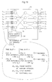
- Figs. 17A and 17B show configuration examples of the incoming line space switch 13 (or, outgoing line space switch 14).
- Figs. 17A and 17B show cases where the incoming line space switch 13 is composed of a bus.
- incoming line space switch (and outgoing line space switch) with a simplified configuration will be implemented.
- Fig. 17A shows a case of a centralized bus configuration
- Fig. 17B shows a case of a decentralized bus configuration.
- Fig. 18 shows another example of the incoming line space switch 13 (and the outgoing line space switch 14).
- Fig. 18 there is shown a case where a cross point switch is used. By using the cross point switch, it is possible that the cell is written independently in the buffer memory at a different timing among the incoming lines.
- Fig. 19 shows another example of the incoming line space switch.
- Fig. 19 there is shown a case where a Banyan switch is used.
- the Banyan switch By using the Banyan switch, the high-speed operation can be implemented.
- the sort network like a Batcher network can be added to the front stage of the Banyan switch.
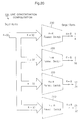
- Fig. 20 is a conceptional view when a large-scale cell switching system is configured by using the above-stated cell switching apparatus.
- a plurality of cell switching apparatuses 200 is provided.
- four cell switching apparatuses 200 are arranged in parallel.
- Fig. 21 shows a relationship table between the maximum number of incoming lines calculated from the number of outgoing lines and the number of buffer memories. In the condition that the number of outgoing lines is fixed to 8, if the number of buffer memories p is changed, the maximum number of incoming lines n is changed as shown in Fig. 21.
- An example shown in Fig. 20 shows a case where four cell switching apparatuses are arranged.
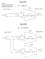
- Figs. 22A, 22B, and 23 show the minimum configuration, the second configuration and the third configuration, respectively. In Figs. 22A, 22B and 23, one, two or three cell switching apparatuses are arranged respectively.
- Each of the cell switching apparatuses 200 utilized in this configuration are totally the same. By arranging a plurality of the same ones, the cell switching systems of different scales, such as 8 x 8, 16 x 16, 24 x 24, and 32 x 32, can be realized.
- the cell switching system whose number of incoming lines equals to the number of outgoing lines. As shown in Fig. 24, it is possible to configure the system whose number of incoming lines is different from the number of outgoing lines by arranging a plurality of cell switching apparatuses 200.
- the arriving cells are not necessarily transmitted to the outgoing lines in the cell switching apparatus.
- the first cell switching apparatus 200 all the cells are coming from the 32 number of incoming lines. However, only the cell switching of the cell whose destinations are the first to the eighth outgoing lines is implemented. Accordingly, only the cells for the first to eighth outgoing lines are selected among the arrived cells. Then, the other cells, i.e., the cells for the ninth to the thirty-second outgoing lines are discarded in the first cell switching apparatus 200.
- the second cell switching apparatus only the cells for the ninth to the sixteenth outgoing lines are selectively switched. Then, the cell whose destinations are the first to the eighth and the seventeenth to the thirty second outgoing lines are discarded in the second cell switching apparatus. Such process of discarding is executed in the header processing circuit or the writing-buffer selective circuit.
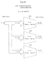
- Figs. 25 to 28 there is shown a explanation of the buffer size evaluation of line concentration type of shared multi buffer ATM switch.
- F the number of the unit switches (also called as the funnel switches)
- m the number of outgoing lines
- the configuration of the 32 x 32 ATM switch is as shown in Fig. 25.
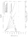
- Fig. 26 shows characteristics of the cell loss probability.
- Fig. 26 shows a relationship between the number of buffers and the cell loss probability. As F decreases, the cell loss probability is proved to be improved according to the effect of sharing the buffer.
- Fig. 27 shows an example of a total buffer size required to attain the cell loss probability 10 ⁇ 5.
- the total buffer size are shown for each of the unit switch.
- the value of F approaches to 1, the amount of buffers to be dedicated in the unit switch excessively increases. Therefore, when it is difficult to configure the shared buffer by a single unit switch with respect to the amount of buffer, it is possible to configure the ATM switch by arranging a plurality of small unit switches such as 32 x 16 or 32 x 8 ATM switches. Accordingly, it is possible for ATM switch to keep the sharing effect of buffers and excel in the extensibility.
Landscapes
- Engineering & Computer Science (AREA)
- Computer Networks & Wireless Communication (AREA)
- Signal Processing (AREA)
- Physics & Mathematics (AREA)
- Mathematical Physics (AREA)
- Data Exchanges In Wide-Area Networks (AREA)
Applications Claiming Priority (3)
| Application Number | Priority Date | Filing Date | Title |
|---|---|---|---|
| JP21024094A JP3269273B2 (ja) | 1994-09-02 | 1994-09-02 | セル交換装置及びセル交換システム |
| JP210240/94 | 1994-09-02 | ||
| JP21024094 | 1994-09-02 |
Publications (3)
| Publication Number | Publication Date |
|---|---|
| EP0700187A2 true EP0700187A2 (de) | 1996-03-06 |
| EP0700187A3 EP0700187A3 (de) | 1999-11-10 |
| EP0700187B1 EP0700187B1 (de) | 2005-12-21 |
Family
ID=16586109
Family Applications (1)
| Application Number | Title | Priority Date | Filing Date |
|---|---|---|---|
| EP95113382A Expired - Lifetime EP0700187B1 (de) | 1994-09-02 | 1995-08-25 | Verfahren und Vorrichtung zum Vermittlen von Zellen |
Country Status (5)
| Country | Link |
|---|---|
| US (1) | US5619495A (de) |
| EP (1) | EP0700187B1 (de) |
| JP (1) | JP3269273B2 (de) |
| CA (1) | CA2156642A1 (de) |
| DE (1) | DE69534698T2 (de) |
Cited By (6)
| Publication number | Priority date | Publication date | Assignee | Title |
|---|---|---|---|---|
| WO1998002013A1 (en) * | 1996-07-09 | 1998-01-15 | International Business Machines Corporation | Switching device, method and apparatus |
| FR2771573A1 (fr) * | 1997-11-27 | 1999-05-28 | Alsthom Cge Alcatel | Element de commutation de paquets a memoires tampons |
| WO2001017178A1 (en) * | 1999-08-31 | 2001-03-08 | Mosaid Technologies Incorporated | Method and apparatus for an interleaved non-blocking packet buffer |
| EP0947078A4 (de) * | 1996-12-16 | 2001-08-29 | Juniper Networks | Schnelle vermittlungsvorrichtung |
| EP1011229A3 (de) * | 1998-12-14 | 2004-04-28 | Lucent Technologies Inc. | RAM Basiertes Mehrtoriges Querverbindungssystem |
| DE19824799B4 (de) * | 1997-06-11 | 2005-01-27 | Samsung Electronics Co., Ltd., Suwon | Eine ATM-Vermittlung und ein Verfahren zur Bestimmung von Pufferschwellwerten |
Families Citing this family (13)
| Publication number | Priority date | Publication date | Assignee | Title |
|---|---|---|---|---|
| FR2736737B1 (fr) * | 1995-07-12 | 1997-08-14 | Alcatel Nv | Dispositif de gestion de relations entre des objets |
| US6046982A (en) * | 1997-03-18 | 2000-04-04 | Cabletron Systems, Inc. | Method and apparatus for reducing data loss in data transfer devices |
| US6563837B2 (en) | 1998-02-10 | 2003-05-13 | Enterasys Networks, Inc. | Method and apparatus for providing work-conserving properties in a non-blocking switch with limited speedup independent of switch size |
| US6865154B1 (en) | 1998-01-12 | 2005-03-08 | Enterasys Networks, Inc. | Method and apparatus for providing bandwidth and delay guarantees in combined input-output buffered crossbar switches that implement work-conserving arbitration algorithms |
| US6112251A (en) | 1998-01-13 | 2000-08-29 | Cabletron Systems, Inc. | Virtual local network for sending multicast transmissions to trunk stations |
| US6469987B1 (en) | 1998-01-13 | 2002-10-22 | Enterasys Networks, Inc. | Virtual local area network with trunk stations |
| US6301224B1 (en) | 1998-01-13 | 2001-10-09 | Enterasys Networks, Inc. | Network switch with panic mode |
| US6526052B1 (en) | 1998-12-23 | 2003-02-25 | Enterasys Networks, Inc. | Virtual local area networks having rules of precedence |
| US6822966B2 (en) | 1999-03-01 | 2004-11-23 | Enterasys Networks, Inc. | Allocating buffers for data transmission in a network communication device |
| JP3628204B2 (ja) * | 1999-03-10 | 2005-03-09 | 沖電気工業株式会社 | 帯域管理回路 |
| US6973092B1 (en) * | 2000-07-28 | 2005-12-06 | Marconi Intellectual Property (Ringfence), Inc. | Dynamic queue utilization |
| US7082127B1 (en) * | 2000-07-28 | 2006-07-25 | Marconi Intellectual Property (Ringfence), Inc. | Synchronous dynamic register updating across a distributed system |
| US7260104B2 (en) * | 2001-12-19 | 2007-08-21 | Computer Network Technology Corporation | Deferred queuing in a buffered switch |
Family Cites Families (10)
| Publication number | Priority date | Publication date | Assignee | Title |
|---|---|---|---|---|
| US4630258A (en) * | 1984-10-18 | 1986-12-16 | Hughes Aircraft Company | Packet switched multiport memory NXM switch node and processing method |
| JPS6364439A (ja) * | 1986-09-04 | 1988-03-22 | Nippon Telegr & Teleph Corp <Ntt> | 共通メモリ管理方式 |
| JPH073977B2 (ja) * | 1986-09-10 | 1995-01-18 | 日本電信電話株式会社 | パケツト交換方式 |
| JP2852053B2 (ja) * | 1988-08-15 | 1999-01-27 | 株式会社日立製作所 | パケット交換装置 |
| JP2695916B2 (ja) * | 1989-05-18 | 1998-01-14 | 株式会社東芝 | セルスイッチ |
| DE69032498T2 (de) * | 1989-10-23 | 1999-03-04 | Mitsubishi Denki K.K., Tokio/Tokyo | Zellenvermittlungseinrichtung |
| JPH03205937A (ja) * | 1990-01-05 | 1991-09-09 | Hitachi Ltd | パケット交換機の流量制御装置および制御方法 |
| JPH05199574A (ja) * | 1992-01-20 | 1993-08-06 | Nippon Telegr & Teleph Corp <Ntt> | Atmクロスコネクトスイッチ回路 |
| JPH066370A (ja) * | 1992-06-18 | 1994-01-14 | Hitachi Ltd | パケットスイッチングシステム |
| JPH06120973A (ja) * | 1992-10-06 | 1994-04-28 | Nippon Telegr & Teleph Corp <Ntt> | Atmクロスコネクト回路 |
-
1994
- 1994-09-02 JP JP21024094A patent/JP3269273B2/ja not_active Expired - Fee Related
-
1995
- 1995-08-21 US US08/517,169 patent/US5619495A/en not_active Expired - Fee Related
- 1995-08-22 CA CA 2156642 patent/CA2156642A1/en not_active Abandoned
- 1995-08-25 DE DE1995634698 patent/DE69534698T2/de not_active Expired - Fee Related
- 1995-08-25 EP EP95113382A patent/EP0700187B1/de not_active Expired - Lifetime
Non-Patent Citations (1)
| Title |
|---|
| None |
Cited By (11)
| Publication number | Priority date | Publication date | Assignee | Title |
|---|---|---|---|---|
| WO1998002013A1 (en) * | 1996-07-09 | 1998-01-15 | International Business Machines Corporation | Switching device, method and apparatus |
| EP0947078A4 (de) * | 1996-12-16 | 2001-08-29 | Juniper Networks | Schnelle vermittlungsvorrichtung |
| DE19824799B4 (de) * | 1997-06-11 | 2005-01-27 | Samsung Electronics Co., Ltd., Suwon | Eine ATM-Vermittlung und ein Verfahren zur Bestimmung von Pufferschwellwerten |
| FR2771573A1 (fr) * | 1997-11-27 | 1999-05-28 | Alsthom Cge Alcatel | Element de commutation de paquets a memoires tampons |
| EP0920157A1 (de) * | 1997-11-27 | 1999-06-02 | Alcatel | Verwaltungseinrichtung eines gemeinsamen Pufferspeichers |
| US6728256B1 (en) | 1997-11-27 | 2004-04-27 | Alcatel | Shared buffer control device |
| EP1011229A3 (de) * | 1998-12-14 | 2004-04-28 | Lucent Technologies Inc. | RAM Basiertes Mehrtoriges Querverbindungssystem |
| WO2001017178A1 (en) * | 1999-08-31 | 2001-03-08 | Mosaid Technologies Incorporated | Method and apparatus for an interleaved non-blocking packet buffer |
| GB2371443A (en) * | 1999-08-31 | 2002-07-24 | Mosaid Technologies Inc | Method and apparatus for an interleaved non-blocking packet buffer |
| GB2371443B (en) * | 1999-08-31 | 2004-02-11 | Mosaid Technologies Inc | Method and apparatus for an interleaved non-blocking packet buffer |
| US6711170B1 (en) | 1999-08-31 | 2004-03-23 | Mosaid Technologies, Inc. | Method and apparatus for an interleaved non-blocking packet buffer |
Also Published As
| Publication number | Publication date |
|---|---|
| EP0700187A3 (de) | 1999-11-10 |
| US5619495A (en) | 1997-04-08 |
| JPH0879271A (ja) | 1996-03-22 |
| DE69534698D1 (de) | 2006-01-26 |
| CA2156642A1 (en) | 1996-03-03 |
| EP0700187B1 (de) | 2005-12-21 |
| JP3269273B2 (ja) | 2002-03-25 |
| DE69534698T2 (de) | 2006-09-28 |
Similar Documents
| Publication | Publication Date | Title |
|---|---|---|
| EP0700187B1 (de) | Verfahren und Vorrichtung zum Vermittlen von Zellen | |
| US5991295A (en) | Digital switch | |
| CA2112528C (en) | Packet switching system for forwarding packets from input buffers using idle/busy status of output buffers | |
| EP0606322B1 (de) | Atm-breitbandkoppelfeldeinrichtung mit gepufferten eingängen | |
| US4926416A (en) | Method and facilities for hybrid packet switching | |
| US6876629B2 (en) | Rate-controlled multi-class high-capacity packet switch | |
| CA2049182C (en) | Traffic shaping method and circuit | |
| US5996019A (en) | Network link access scheduling using a plurality of prioritized lists containing queue identifiers | |
| EP0858718B1 (de) | Verbesserungen in oder sich beziehend auf einer atm-vermittlungsstelle | |
| US4788679A (en) | Packet switch with variable data transfer rate links | |
| US5896380A (en) | Multi-core ATM switch with cells in the core from an inlet for an outlet being aligned | |
| US6611527B1 (en) | Packet switching apparatus with a common buffer | |
| US6757791B1 (en) | Method and apparatus for reordering packet data units in storage queues for reading and writing memory | |
| US20040151197A1 (en) | Priority queue architecture for supporting per flow queuing and multiple ports | |
| US5649217A (en) | Switching system having control circuit and plural buffer memories for data exchange in asynchronous transfer mode | |
| EP0828403B1 (de) | Verbesserungen in oder sich beziehend auf eine ATM-Vermittlungsstelle | |
| IL124011A (en) | Atm switch | |
| WO1999051000A1 (en) | Ampic dram system in a telecommunication switch | |
| US6061358A (en) | Data communication system utilizing a scalable, non-blocking, high bandwidth central memory controller and method | |
| JPH11266272A (ja) | 共用バッファ制御装置 | |
| US6046982A (en) | Method and apparatus for reducing data loss in data transfer devices | |
| US6493315B1 (en) | ATM switch for routing different cell types | |
| US5463622A (en) | Control unit for the common memory of an ATM node | |
| EP0870415B1 (de) | Vermittlungseinrichtung | |
| US20070140232A1 (en) | Self-steering Clos switch |
Legal Events
| Date | Code | Title | Description |
|---|---|---|---|
| PUAI | Public reference made under article 153(3) epc to a published international application that has entered the european phase |
Free format text: ORIGINAL CODE: 0009012 |
|
| AK | Designated contracting states |
Kind code of ref document: A2 Designated state(s): DE FR GB SE |
|
| PUAL | Search report despatched |
Free format text: ORIGINAL CODE: 0009013 |
|
| AK | Designated contracting states |
Kind code of ref document: A3 Designated state(s): DE FR GB SE |
|
| 17P | Request for examination filed |
Effective date: 19991027 |
|
| 17Q | First examination report despatched |
Effective date: 20040330 |
|
| GRAP | Despatch of communication of intention to grant a patent |
Free format text: ORIGINAL CODE: EPIDOSNIGR1 |
|
| GRAS | Grant fee paid |
Free format text: ORIGINAL CODE: EPIDOSNIGR3 |
|
| GRAA | (expected) grant |
Free format text: ORIGINAL CODE: 0009210 |
|
| AK | Designated contracting states |
Kind code of ref document: B1 Designated state(s): DE FR GB SE |
|
| REG | Reference to a national code |
Ref country code: GB Ref legal event code: FG4D |
|
| REF | Corresponds to: |
Ref document number: 69534698 Country of ref document: DE Date of ref document: 20060126 Kind code of ref document: P |
|
| PG25 | Lapsed in a contracting state [announced via postgrant information from national office to epo] |
Ref country code: SE Free format text: LAPSE BECAUSE OF FAILURE TO SUBMIT A TRANSLATION OF THE DESCRIPTION OR TO PAY THE FEE WITHIN THE PRESCRIBED TIME-LIMIT Effective date: 20060321 |
|
| RAP2 | Party data changed (patent owner data changed or rights of a patent transferred) |
Owner name: MITSUBISHI DENKI KABUSHIKI KAISHA |
|
| ET | Fr: translation filed | ||
| PLBE | No opposition filed within time limit |
Free format text: ORIGINAL CODE: 0009261 |
|
| STAA | Information on the status of an ep patent application or granted ep patent |
Free format text: STATUS: NO OPPOSITION FILED WITHIN TIME LIMIT |
|
| 26N | No opposition filed |
Effective date: 20060922 |
|
| PGFP | Annual fee paid to national office [announced via postgrant information from national office to epo] |
Ref country code: DE Payment date: 20070823 Year of fee payment: 13 |
|
| PGFP | Annual fee paid to national office [announced via postgrant information from national office to epo] |
Ref country code: GB Payment date: 20070822 Year of fee payment: 13 |
|
| PGFP | Annual fee paid to national office [announced via postgrant information from national office to epo] |
Ref country code: FR Payment date: 20070808 Year of fee payment: 13 |
|
| GBPC | Gb: european patent ceased through non-payment of renewal fee |
Effective date: 20080825 |
|
| REG | Reference to a national code |
Ref country code: FR Ref legal event code: ST Effective date: 20090430 |
|
| PG25 | Lapsed in a contracting state [announced via postgrant information from national office to epo] |
Ref country code: FR Free format text: LAPSE BECAUSE OF NON-PAYMENT OF DUE FEES Effective date: 20080901 Ref country code: DE Free format text: LAPSE BECAUSE OF NON-PAYMENT OF DUE FEES Effective date: 20090303 |
|
| PG25 | Lapsed in a contracting state [announced via postgrant information from national office to epo] |
Ref country code: GB Free format text: LAPSE BECAUSE OF NON-PAYMENT OF DUE FEES Effective date: 20080825 |