EP0701298A2 - Connecteur de montage en surface à faible inductance pout interconnecter de dispositifs de circuits et méthode d'utilisation - Google Patents
Connecteur de montage en surface à faible inductance pout interconnecter de dispositifs de circuits et méthode d'utilisation Download PDFInfo
- Publication number
- EP0701298A2 EP0701298A2 EP95306063A EP95306063A EP0701298A2 EP 0701298 A2 EP0701298 A2 EP 0701298A2 EP 95306063 A EP95306063 A EP 95306063A EP 95306063 A EP95306063 A EP 95306063A EP 0701298 A2 EP0701298 A2 EP 0701298A2
- Authority
- EP
- European Patent Office
- Prior art keywords
- circuit device
- connector
- connectors
- circuit
- mounting pads
- Prior art date
- Legal status (The legal status is an assumption and is not a legal conclusion. Google has not performed a legal analysis and makes no representation as to the accuracy of the status listed.)
- Granted
Links
Images

Classifications
-
- H—ELECTRICITY
- H01—ELECTRIC ELEMENTS
- H01R—ELECTRICALLY-CONDUCTIVE CONNECTIONS; STRUCTURAL ASSOCIATIONS OF A PLURALITY OF MUTUALLY-INSULATED ELECTRICAL CONNECTING ELEMENTS; COUPLING DEVICES; CURRENT COLLECTORS
- H01R12/00—Structural associations of a plurality of mutually-insulated electrical connecting elements, specially adapted for printed circuits, e.g. printed circuit boards [PCB], flat or ribbon cables, or like generally planar structures, e.g. terminal strips, terminal blocks; Coupling devices specially adapted for printed circuits, flat or ribbon cables, or like generally planar structures; Terminals specially adapted for contact with, or insertion into, printed circuits, flat or ribbon cables, or like generally planar structures
- H01R12/50—Fixed connections
- H01R12/51—Fixed connections for rigid printed circuits or like structures
- H01R12/55—Fixed connections for rigid printed circuits or like structures characterised by the terminals
- H01R12/57—Fixed connections for rigid printed circuits or like structures characterised by the terminals surface mounting terminals
-
- H—ELECTRICITY
- H05—ELECTRIC TECHNIQUES NOT OTHERWISE PROVIDED FOR
- H05K—PRINTED CIRCUITS; CASINGS OR CONSTRUCTIONAL DETAILS OF ELECTRIC APPARATUS; MANUFACTURE OF ASSEMBLAGES OF ELECTRICAL COMPONENTS
- H05K3/00—Apparatus or processes for manufacturing printed circuits
- H05K3/36—Assembling printed circuits with other printed circuits
-
- H—ELECTRICITY
- H01—ELECTRIC ELEMENTS
- H01R—ELECTRICALLY-CONDUCTIVE CONNECTIONS; STRUCTURAL ASSOCIATIONS OF A PLURALITY OF MUTUALLY-INSULATED ELECTRICAL CONNECTING ELEMENTS; COUPLING DEVICES; CURRENT COLLECTORS
- H01R12/00—Structural associations of a plurality of mutually-insulated electrical connecting elements, specially adapted for printed circuits, e.g. printed circuit boards [PCB], flat or ribbon cables, or like generally planar structures, e.g. terminal strips, terminal blocks; Coupling devices specially adapted for printed circuits, flat or ribbon cables, or like generally planar structures; Terminals specially adapted for contact with, or insertion into, printed circuits, flat or ribbon cables, or like generally planar structures
- H01R12/70—Coupling devices
- H01R12/71—Coupling devices for rigid printing circuits or like structures
- H01R12/712—Coupling devices for rigid printing circuits or like structures co-operating with the surface of the printed circuit or with a coupling device exclusively provided on the surface of the printed circuit
- H01R12/714—Coupling devices for rigid printing circuits or like structures co-operating with the surface of the printed circuit or with a coupling device exclusively provided on the surface of the printed circuit with contacts abutting directly the printed circuit; Button contacts therefore provided on the printed circuit
-
- H—ELECTRICITY
- H05—ELECTRIC TECHNIQUES NOT OTHERWISE PROVIDED FOR
- H05K—PRINTED CIRCUITS; CASINGS OR CONSTRUCTIONAL DETAILS OF ELECTRIC APPARATUS; MANUFACTURE OF ASSEMBLAGES OF ELECTRICAL COMPONENTS
- H05K3/00—Apparatus or processes for manufacturing printed circuits
- H05K3/36—Assembling printed circuits with other printed circuits
- H05K3/368—Assembling printed circuits with other printed circuits parallel to each other
-
- H—ELECTRICITY
- H05—ELECTRIC TECHNIQUES NOT OTHERWISE PROVIDED FOR
- H05K—PRINTED CIRCUITS; CASINGS OR CONSTRUCTIONAL DETAILS OF ELECTRIC APPARATUS; MANUFACTURE OF ASSEMBLAGES OF ELECTRICAL COMPONENTS
- H05K1/00—Printed circuits
- H05K1/02—Details
- H05K1/14—Structural association of two or more printed circuits
- H05K1/141—One or more single auxiliary printed circuits mounted on a main printed circuit, e.g. modules, adapters
-
- H—ELECTRICITY
- H05—ELECTRIC TECHNIQUES NOT OTHERWISE PROVIDED FOR
- H05K—PRINTED CIRCUITS; CASINGS OR CONSTRUCTIONAL DETAILS OF ELECTRIC APPARATUS; MANUFACTURE OF ASSEMBLAGES OF ELECTRICAL COMPONENTS
- H05K2201/00—Indexing scheme relating to printed circuits covered by H05K1/00
- H05K2201/10—Details of components or other objects attached to or integrated in a printed circuit board
- H05K2201/10227—Other objects, e.g. metallic pieces
- H05K2201/1031—Surface mounted metallic connector elements
-
- H—ELECTRICITY
- H05—ELECTRIC TECHNIQUES NOT OTHERWISE PROVIDED FOR
- H05K—PRINTED CIRCUITS; CASINGS OR CONSTRUCTIONAL DETAILS OF ELECTRIC APPARATUS; MANUFACTURE OF ASSEMBLAGES OF ELECTRICAL COMPONENTS
- H05K2201/00—Indexing scheme relating to printed circuits covered by H05K1/00
- H05K2201/10—Details of components or other objects attached to or integrated in a printed circuit board
- H05K2201/10613—Details of electrical connections of non-printed components, e.g. special leads
- H05K2201/10742—Details of leads
- H05K2201/1075—Shape details
- H05K2201/1084—Notched leads
-
- H—ELECTRICITY
- H05—ELECTRIC TECHNIQUES NOT OTHERWISE PROVIDED FOR
- H05K—PRINTED CIRCUITS; CASINGS OR CONSTRUCTIONAL DETAILS OF ELECTRIC APPARATUS; MANUFACTURE OF ASSEMBLAGES OF ELECTRICAL COMPONENTS
- H05K3/00—Apparatus or processes for manufacturing printed circuits
- H05K3/30—Assembling printed circuits with electric components, e.g. with resistors
- H05K3/32—Assembling printed circuits with electric components, e.g. with resistors electrically connecting electric components or wires to printed circuits
- H05K3/34—Assembling printed circuits with electric components, e.g. with resistors electrically connecting electric components or wires to printed circuits by soldering
- H05K3/341—Surface mounted components
- H05K3/3421—Leaded components
- H05K3/3426—Leaded components characterised by the leads
-
- Y—GENERAL TAGGING OF NEW TECHNOLOGICAL DEVELOPMENTS; GENERAL TAGGING OF CROSS-SECTIONAL TECHNOLOGIES SPANNING OVER SEVERAL SECTIONS OF THE IPC; TECHNICAL SUBJECTS COVERED BY FORMER USPC CROSS-REFERENCE ART COLLECTIONS [XRACs] AND DIGESTS
- Y02—TECHNOLOGIES OR APPLICATIONS FOR MITIGATION OR ADAPTATION AGAINST CLIMATE CHANGE
- Y02P—CLIMATE CHANGE MITIGATION TECHNOLOGIES IN THE PRODUCTION OR PROCESSING OF GOODS
- Y02P70/00—Climate change mitigation technologies in the production process for final industrial or consumer products
- Y02P70/50—Manufacturing or production processes characterised by the final manufactured product
Definitions
- This invention relates to devices for interconnecting circuit devices such as IC packages to circuit boards, circuit boards to circuit boards or substrates and substrates to substrates. Specifically, the invention relates to low inductance surface-mount connectors having advantageous qualities of compactness, low interconnection inductance and mechanical compliance.
- the connectors can be surface mounted by pick-and-place techniques.
- FIG. 1 is a perspective view of a novel low inductance surface-mount connector comprising a metallic rectangular parallelepiped 10 which is hollow along the dimension A (the length).
- the connector advantageously has one or more slots 11 in planes transverse to the length A, the slots extending over three of the four sidewalls. The remaining sidewall 12 is unslotted to hold the connector together.
- the parallelepiped is hollow along its x-axis (length, A), and the slots 11 are in the y-z plane.
- the mounting surfaces are chosen such that the two sidewalls that are perpendicular to the plane of the circuit devices are both slotted.
- the mounting surfaces are the opposite sidewalls in the x-y plane, such as sidewalls 12. The connector thus provides electrical connectivity in the z-direction.
- the connector height B is advantageously chosen to be greater than the height of the tallest component on the interconnect side of the circuit devices to be interconnected so that contact between the two circuit devices is only through the connectors.
- B is larger in height than the tallest component by about 0.010'' to 0.015''.
- a minimum metal thickness t is selected on the basis of mechanical device stability and manufacturability.
- t selected on these bases meets the compliance requirements in the y-direction.
- typical metal thicknesses are in the range 0.005'' to 0.020''.
- the metal is plated with a thin layer (typically 0.0002") of copper or nickel, followed by solder to enhance solderability.
- the number n of equally spaced slots 11, and hence the length A is determined by the maximum inductance requirement.
- the device provides 2 (n+1) conductive regions 13 which are electrically parallel conductive paths in the z-direction, each with width a and thickness t.
- a ⁇ B For placement stability, a further restriction on A is A ⁇ B.
- the device of FIG. 1 is shown without a seam. It can be conveniently fabricated from an extruded rectangular metal tube by cutting slots in the tubing and cutting off the ends to desired length A.
- the inductance associated with the connector is a function of the parameters B, C, t, s, a and n. With the first five parameters determined primarily from mechanical considerations, n (and thus A) can be varied to meet the inductive requirements. In general, the inductance monotonically decreases with increasing n.
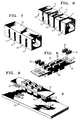
- FIG. 8 is a perspective view showing surface mount connectors 10 being mounted on a first circuit device 51.
- the circuit device 51 comprises a substrate or circuit board 52, one or more circuit components 53 and one or more mounting pads 54 for receiving connectors 10.
- both connectors 10 and pads 54 are pre-coated with solder.
- the height of connectors 10 is greater than the height of any circuit component 53.
- the connectors can then be placed on the pads by standard pick-and-place techniques and can be soldered to the pads in a conventional solder reflow step.
- the next step shown in FIG. 9 is to mount the first circuit device 51 onto a second circuit device 60.
- Device 60 can also comprise a package or substrate or circuit board 61 and is preferably the larger area circuit device of the two.
- circuit device 60 is provided with solder pads 62 appropriate in size and distribution for receiving the connectors mounted on circuit device 51.
- the pads 62 are preferably pre-coated with solder, and circuit device 51 can be applied on device 60 using pick-and-place techniques with connectors 10 in registration with pads 62.
- the two circuit devices can then be interconnected by solder reflow. The result is an interconnected composite device having advantageous qualities of compactness, low interconnection inductance and mechanical compliance with respect to thermal mismatch.
- the principles of the invention were used to design and fabricate devices to meet the requirements of a specific application.
- the height of the tallest component on the interconnected side of the board was H c ⁇ 0.050''.
- the mechanical requirement was compliance under solder reflow and high operating temperatures, in spite of the large TCE mismatch.
- the electrical requirement was a maximum inductance per interconnect of 0.150 nH.
- a very small interconnect footprint was necessary: the size of the FR4 board was approximately 0.5'' ⁇ 2.0'', and much of the interconnect-side area was needed for other components.
- a 0.030'' (B/a ⁇ 2).
- N and hence the device length A, was then determined by exact inductance calculations, using the method described earlier, on the basis of the minimum N necessary to meet the inductance requirement of L ⁇ 0.150nH.
- the device length A was 0.110''in each case.
- the device footprint was 0.110'' ⁇
- Connectors with the above dimensions were fabricated from rectangular metallic strips with etched slots.
- the base metals were (i) brass, (ii) a commercial phosphor-bronze alloy, C 51000, comprising 95% Cu and 5% Sn.
- Strip thicknesses were 0.008'' and 0.007''.
- the 0.008'' parts (brass) were plated with 0.0001'' thick Ni.
- the 0.007" parts (phosphor-bronze) were plates with 0.0001" Ni, followed by 0.0002" solder.
- a two-step tool and die arrangement was used in a hand press to form the strips into devices, as shown in FIG. 2, with the required dimensions.
- test boards were made out of FR4 (0.030'' thick) and 96% Al2O3 (0.050'' thick).
- the FR4 boards each 3.2'' long and 0.6'' wide, were of two types, "x" and "y", depending on the pattern of solder pads on the interconnect side. These solder pads measured 0.125'' ⁇ 0.075'', to accommodate the connectors.
- the x-type boards designed for testing compliance in the device x-direction, had a pad pattern consisting of two rows of 7 pads each. The pads were oriented such that the device x-direction would be parallel to the board length.
- the center-to-center distance between pads was 0.500" along the board length, and 0.425" along the board width.
- the y-type boards designed for testing compliance in the device y-direction, had a pad pattern identical to the x-types, except that the pad orientation was perpendicular, i.e., the device y-direction was parallel to the board length.
- the pad center-to-center distance was again 0.500'' along the board length, and 0.375'' along the board width.
- the alumina (Al2O3) boards, each 3.73'' long, and 2.00'' wide, were also made in "x" and "y" types, each type having a pad pattern identical to the corresponding FR4 board. Note that the test boards were designed to test either x- or y-direction compliance over a maximum interconnect-to-interconnect distance of 3.00''.
- the exemplary connector device provides a true surface mountable 0.062" long interconnect between two boards or packages that:
- PGAs pin grid arrays
- J leads Two exemplary prior art approaches to meeting the application requirements are pin grid arrays (PGAs) and compliant J leads.
- PGAs Commonly used to provide interconnect between ceramic (Al2O3) packages and FR4 boards, PGAs comprise pins brazed in an area array onto the package. The package is then thru-hole mounted onto the FR4 board, or mounted into a multi-hole socket. The pins are typically 0.018" in diameter, and 0.100'' long. Typical x- and y-pitch in the array is 0.100''. Multiple pins are connected in parallel to provide the required low inductance per I/O for a particular application.
- J leads are a relatively recent approach to providing compliant interconnects in which the first-board to second-board connection is surface mountable.
- U.S. Patent 4,605,278. It comprises "J" shaped leads, 0.018'' ⁇ 0.007" in cross-section, each with a solderable clip for attachment to the edge of the first board. At least 0.062" of the edges of both top and bottom sides of the board are taken up for attachment. These leads can be placed on 0.50" centers.
Landscapes
- Engineering & Computer Science (AREA)
- Manufacturing & Machinery (AREA)
- Microelectronics & Electronic Packaging (AREA)
- Coupling Device And Connection With Printed Circuit (AREA)
- Multi-Conductor Connections (AREA)
- Combinations Of Printed Boards (AREA)
Applications Claiming Priority (2)
| Application Number | Priority Date | Filing Date | Title |
|---|---|---|---|
| US302559 | 1994-09-08 | ||
| US08/302,559 US5588848A (en) | 1994-09-08 | 1994-09-08 | Low inductance surface-mount connectors for interconnecting circuit devices and method for using same |
Publications (3)
| Publication Number | Publication Date |
|---|---|
| EP0701298A2 true EP0701298A2 (fr) | 1996-03-13 |
| EP0701298A3 EP0701298A3 (fr) | 1997-05-02 |
| EP0701298B1 EP0701298B1 (fr) | 2000-03-22 |
Family
ID=23168264
Family Applications (1)
| Application Number | Title | Priority Date | Filing Date |
|---|---|---|---|
| EP95306063A Expired - Lifetime EP0701298B1 (fr) | 1994-09-08 | 1995-08-30 | Connecteur de montage en surface à faible inductance pout interconnecter de dispositifs de circuits et méthode d'utilisation |
Country Status (8)
| Country | Link |
|---|---|
| US (1) | US5588848A (fr) |
| EP (1) | EP0701298B1 (fr) |
| JP (1) | JP3168242B2 (fr) |
| KR (1) | KR960013144A (fr) |
| AU (1) | AU682622B2 (fr) |
| CA (1) | CA2155257C (fr) |
| DE (1) | DE69515764T2 (fr) |
| TW (1) | TW271014B (fr) |
Cited By (3)
| Publication number | Priority date | Publication date | Assignee | Title |
|---|---|---|---|---|
| US6146155A (en) * | 1997-09-16 | 2000-11-14 | 3M Innovative Properties Company | Recyclable locater device for board mounted connectors |
| DE10003696A1 (de) * | 2000-01-28 | 2001-08-09 | Eupec Gmbh & Co Kg | Abnahmeeinrichtung für elektrischen Strom |
| CN110875530A (zh) * | 2018-08-31 | 2020-03-10 | 日本航空电子工业株式会社 | 焊接部件 |
Families Citing this family (25)
| Publication number | Priority date | Publication date | Assignee | Title |
|---|---|---|---|---|
| JPH11186688A (ja) * | 1997-10-14 | 1999-07-09 | Murata Mfg Co Ltd | ハイブリッドicおよびそれを用いた電子装置 |
| US6175500B1 (en) * | 1998-09-22 | 2001-01-16 | Lucent Technologies Inc. | Surface mount thermal connections |
| US6189203B1 (en) | 1999-04-08 | 2001-02-20 | Lucent Technologies Inc. | Method of manufacturing a surface mountable power supply module |
| US6310301B1 (en) | 1999-04-08 | 2001-10-30 | Randy T. Heinrich | Inter-substrate conductive mount for a circuit board, circuit board and power magnetic device employing the same |
| US6503088B2 (en) * | 2000-12-15 | 2003-01-07 | Di/Dt, Inc. | I-channel surface-mount connector with extended flanges |
| US6750396B2 (en) * | 2000-12-15 | 2004-06-15 | Di/Dt, Inc. | I-channel surface-mount connector |
| DE10215985A1 (de) * | 2002-04-11 | 2003-11-06 | Siemens Ag | Hochstrom-Kontaktelement zur Befestigung an einer Leiterplattenanordnung und Verwendung eines Hochstrom-Kontaktelements |
| US6786736B2 (en) | 2002-08-23 | 2004-09-07 | Artesyn Technologies, Inc. | Surface mount interconnect and device including same |
| US20040048498A1 (en) * | 2002-09-06 | 2004-03-11 | Hong Huang | Metallic surface mount technology power connector |
| US7065351B2 (en) | 2003-01-30 | 2006-06-20 | Qualcomm Incorporated | Event-triggered data collection |
| US7123928B2 (en) * | 2003-07-21 | 2006-10-17 | Qualcomm Incorporated | Method and apparatus for creating and using a base station almanac for position determination |
| DE10333566A1 (de) * | 2003-07-23 | 2005-02-10 | eupec Europäische Gesellschaft für Leistungshalbleiter mbH | Verbindungsanordnung |
| WO2005106523A1 (fr) | 2004-04-02 | 2005-11-10 | Qualcomm Incorporated | Procedes et appareils destines a des systemes de determination de position assistes par balises |
| US20050277313A1 (en) * | 2004-06-09 | 2005-12-15 | Aldrin Pangilinan | Surface mountable pin assembly for a printed circuit board |
| US20060046525A1 (en) * | 2004-08-27 | 2006-03-02 | Allan Mark | Printed circuit board type connector using surface mount and through hole technologies |
| JP4676855B2 (ja) * | 2005-10-03 | 2011-04-27 | ローム株式会社 | ハイブリッド集積回路装置とその製造方法 |
| US7740066B2 (en) * | 2008-01-25 | 2010-06-22 | Halliburton Energy Services, Inc. | Additives for high alumina cements and associated methods |
| US8478228B2 (en) | 2008-10-20 | 2013-07-02 | Qualcomm Incorporated | Mobile receiver with location services capability |
| US8600297B2 (en) | 2009-07-28 | 2013-12-03 | Qualcomm Incorporated | Method and system for femto cell self-timing and self-locating |
| USD648959S1 (en) * | 2010-10-25 | 2011-11-22 | Design Force Ab | Display and sales unit |
| USD697786S1 (en) * | 2012-10-27 | 2014-01-21 | Joel McMahon | Desktop display cord holder |
| USD749292S1 (en) * | 2014-10-14 | 2016-02-16 | Time And Oak, Inc. | Beverage flavoring element |
| USD747582S1 (en) * | 2015-05-01 | 2016-01-12 | Ronald Kenneth Weller | Seat belt cleaner |
| JP6542573B2 (ja) * | 2015-05-11 | 2019-07-10 | フジコン株式会社 | 基板端子 |
| JP6572820B2 (ja) * | 2016-04-25 | 2019-09-11 | 富士通株式会社 | 電源供給構造 |
Family Cites Families (6)
| Publication number | Priority date | Publication date | Assignee | Title |
|---|---|---|---|---|
| FR2192437B1 (fr) * | 1972-07-10 | 1974-10-25 | Radiotechnique Compelec | |
| US4605278A (en) * | 1985-05-24 | 1986-08-12 | North American Specialties Corporation | Solder-bearing leads |
| US4629267A (en) * | 1984-10-12 | 1986-12-16 | Gte Communication Systems Corporation | Circuit terminating device |
| JPS6427293A (en) * | 1987-07-22 | 1989-01-30 | Fujitsu Ltd | Method of mount chip component |
| US4915652A (en) * | 1989-06-12 | 1990-04-10 | Thomas & Betts Corporation | Shielded electrical connector |
| US5256086A (en) * | 1992-12-04 | 1993-10-26 | Molex Incorporated | Electrical connector shield and method of fabricating same |
-
1994
- 1994-09-08 US US08/302,559 patent/US5588848A/en not_active Expired - Lifetime
-
1995
- 1995-01-24 TW TW084100617A patent/TW271014B/zh active
- 1995-08-03 CA CA002155257A patent/CA2155257C/fr not_active Expired - Fee Related
- 1995-08-30 DE DE69515764T patent/DE69515764T2/de not_active Expired - Fee Related
- 1995-08-30 EP EP95306063A patent/EP0701298B1/fr not_active Expired - Lifetime
- 1995-09-01 AU AU30404/95A patent/AU682622B2/en not_active Ceased
- 1995-09-05 KR KR1019950028929A patent/KR960013144A/ko not_active Abandoned
- 1995-09-07 JP JP25453895A patent/JP3168242B2/ja not_active Expired - Fee Related
Cited By (5)
| Publication number | Priority date | Publication date | Assignee | Title |
|---|---|---|---|---|
| US6146155A (en) * | 1997-09-16 | 2000-11-14 | 3M Innovative Properties Company | Recyclable locater device for board mounted connectors |
| DE10003696A1 (de) * | 2000-01-28 | 2001-08-09 | Eupec Gmbh & Co Kg | Abnahmeeinrichtung für elektrischen Strom |
| EP1120860A3 (fr) * | 2000-01-28 | 2003-04-09 | eupec GmbH, Europäische Gesellschaft für Leistungshalbleiter mbH & Co.KG | Socle pour courant électrique |
| CN110875530A (zh) * | 2018-08-31 | 2020-03-10 | 日本航空电子工业株式会社 | 焊接部件 |
| CN110875530B (zh) * | 2018-08-31 | 2021-04-20 | 日本航空电子工业株式会社 | 焊接部件 |
Also Published As
| Publication number | Publication date |
|---|---|
| AU3040495A (en) | 1996-03-21 |
| EP0701298A3 (fr) | 1997-05-02 |
| JPH08195234A (ja) | 1996-07-30 |
| KR960013144A (ko) | 1996-04-20 |
| DE69515764D1 (de) | 2000-04-27 |
| JP3168242B2 (ja) | 2001-05-21 |
| TW271014B (en) | 1996-02-21 |
| US5588848A (en) | 1996-12-31 |
| EP0701298B1 (fr) | 2000-03-22 |
| AU682622B2 (en) | 1997-10-09 |
| DE69515764T2 (de) | 2000-08-31 |
| CA2155257A1 (fr) | 1996-03-09 |
| CA2155257C (fr) | 1999-12-21 |
Similar Documents
| Publication | Publication Date | Title |
|---|---|---|
| EP0701298B1 (fr) | Connecteur de montage en surface à faible inductance pout interconnecter de dispositifs de circuits et méthode d'utilisation | |
| EP1342294B1 (fr) | Connecteur en i pour montage en surface | |
| US4620761A (en) | High density chip socket | |
| EP0237808A2 (fr) | Plaquettes multicouches interposable pour alimenter des modules à puces à fort courant | |
| EP0575806A2 (fr) | Empaquetage pour puces à circuit intégrés | |
| EP0717471A2 (fr) | Connecteur à haute densité et courants élevés du type plot de contact à plot de contact, comprenant des contacts à ressort | |
| US6765805B2 (en) | Circuit component | |
| EP1446993B1 (fr) | Connecteur monte en surface presentant un canal en i et des rebords allonges et methode d'interconnexion de circuits imprimes | |
| US6692269B2 (en) | Circuit module with universal connectivity | |
| US6815614B1 (en) | Arrangement for co-planar vertical surface mounting of subassemblies on a mother board | |
| US6984156B2 (en) | Connector for surface mounting subassemblies vertically on a mother board and assemblies comprising the same | |
| JPH11135217A (ja) | Icソケット | |
| WO1991005369A1 (fr) | Dissipateur thermique pour dispositifs semi-conducteurs | |
| JP2697656B2 (ja) | チップ部品立体実装用ソケット | |
| JP2004259746A (ja) | 表面実装用基板及びアンテナ装置 | |
| JPH0562065U (ja) | ハイブリットicの実装構造 | |
| JPH0669623A (ja) | 表面実装構造およびそのための部品 |
Legal Events
| Date | Code | Title | Description |
|---|---|---|---|
| PUAI | Public reference made under article 153(3) epc to a published international application that has entered the european phase |
Free format text: ORIGINAL CODE: 0009012 |
|
| AK | Designated contracting states |
Kind code of ref document: A2 Designated state(s): DE FR GB |
|
| RIN1 | Information on inventor provided before grant (corrected) |
Inventor name: ROY, APURBA Inventor name: SHEWMAKE, STEVEN AUBREY Inventor name: LAW, RONALD LEAVITT |
|
| PUAL | Search report despatched |
Free format text: ORIGINAL CODE: 0009013 |
|
| AK | Designated contracting states |
Kind code of ref document: A3 Designated state(s): DE FR GB |
|
| 17P | Request for examination filed |
Effective date: 19971016 |
|
| 17Q | First examination report despatched |
Effective date: 19980826 |
|
| GRAG | Despatch of communication of intention to grant |
Free format text: ORIGINAL CODE: EPIDOS AGRA |
|
| GRAG | Despatch of communication of intention to grant |
Free format text: ORIGINAL CODE: EPIDOS AGRA |
|
| GRAH | Despatch of communication of intention to grant a patent |
Free format text: ORIGINAL CODE: EPIDOS IGRA |
|
| GRAH | Despatch of communication of intention to grant a patent |
Free format text: ORIGINAL CODE: EPIDOS IGRA |
|
| GRAA | (expected) grant |
Free format text: ORIGINAL CODE: 0009210 |
|
| RIN1 | Information on inventor provided before grant (corrected) |
Inventor name: ROY, APURBA Inventor name: SHEWMAKE, STEVEN AUBREY Inventor name: LAW, RONALD LEAVITT |
|
| AK | Designated contracting states |
Kind code of ref document: B1 Designated state(s): DE FR GB |
|
| RIC1 | Information provided on ipc code assigned before grant |
Free format text: 7H 01R 12/04 A, 7H 01R 9/05 B, 7H 05K 3/36 B |
|
| REF | Corresponds to: |
Ref document number: 69515764 Country of ref document: DE Date of ref document: 20000427 |
|
| ET | Fr: translation filed | ||
| PGFP | Annual fee paid to national office [announced via postgrant information from national office to epo] |
Ref country code: FR Payment date: 20000624 Year of fee payment: 6 |
|
| PGFP | Annual fee paid to national office [announced via postgrant information from national office to epo] |
Ref country code: GB Payment date: 20000801 Year of fee payment: 6 |
|
| PGFP | Annual fee paid to national office [announced via postgrant information from national office to epo] |
Ref country code: DE Payment date: 20000929 Year of fee payment: 6 |
|
| PLBE | No opposition filed within time limit |
Free format text: ORIGINAL CODE: 0009261 |
|
| STAA | Information on the status of an ep patent application or granted ep patent |
Free format text: STATUS: NO OPPOSITION FILED WITHIN TIME LIMIT |
|
| 26N | No opposition filed | ||
| PG25 | Lapsed in a contracting state [announced via postgrant information from national office to epo] |
Ref country code: GB Free format text: LAPSE BECAUSE OF NON-PAYMENT OF DUE FEES Effective date: 20010830 |
|
| PG25 | Lapsed in a contracting state [announced via postgrant information from national office to epo] |
Ref country code: FR Free format text: LAPSE BECAUSE OF NON-PAYMENT OF DUE FEES Effective date: 20020430 |
|
| PG25 | Lapsed in a contracting state [announced via postgrant information from national office to epo] |
Ref country code: DE Free format text: LAPSE BECAUSE OF NON-PAYMENT OF DUE FEES Effective date: 20020501 |
|
| REG | Reference to a national code |
Ref country code: FR Ref legal event code: ST |