EP0702101A2 - MBE System and semiconductor device fabricated using same - Google Patents
MBE System and semiconductor device fabricated using same Download PDFInfo
- Publication number
- EP0702101A2 EP0702101A2 EP95114404A EP95114404A EP0702101A2 EP 0702101 A2 EP0702101 A2 EP 0702101A2 EP 95114404 A EP95114404 A EP 95114404A EP 95114404 A EP95114404 A EP 95114404A EP 0702101 A2 EP0702101 A2 EP 0702101A2
- Authority
- EP
- European Patent Office
- Prior art keywords
- chamber
- layer
- compound semiconductor
- layers
- semiconductor device
- Prior art date
- Legal status (The legal status is an assumption and is not a legal conclusion. Google has not performed a legal analysis and makes no representation as to the accuracy of the status listed.)
- Withdrawn
Links
Images

Classifications
-
- H—ELECTRICITY
- H10—SEMICONDUCTOR DEVICES; ELECTRIC SOLID-STATE DEVICES NOT OTHERWISE PROVIDED FOR
- H10H—INORGANIC LIGHT-EMITTING SEMICONDUCTOR DEVICES HAVING POTENTIAL BARRIERS
- H10H20/00—Individual inorganic light-emitting semiconductor devices having potential barriers, e.g. light-emitting diodes [LED]
- H10H20/01—Manufacture or treatment
- H10H20/011—Manufacture or treatment of bodies, e.g. forming semiconductor layers
- H10H20/012—Manufacture or treatment of bodies, e.g. forming semiconductor layers having light-emitting regions comprising only Group II-IV materials
-
- H—ELECTRICITY
- H10—SEMICONDUCTOR DEVICES; ELECTRIC SOLID-STATE DEVICES NOT OTHERWISE PROVIDED FOR
- H10P—GENERIC PROCESSES OR APPARATUS FOR THE MANUFACTURE OR TREATMENT OF DEVICES COVERED BY CLASS H10
- H10P14/00—Formation of materials, e.g. in the shape of layers or pillars
- H10P14/20—Formation of materials, e.g. in the shape of layers or pillars of semiconductor materials
- H10P14/29—Formation of materials, e.g. in the shape of layers or pillars of semiconductor materials characterised by the substrates
- H10P14/2901—Materials
- H10P14/2907—Materials being Group IIIA-VA materials
- H10P14/2911—Arsenides
-
- H—ELECTRICITY
- H10—SEMICONDUCTOR DEVICES; ELECTRIC SOLID-STATE DEVICES NOT OTHERWISE PROVIDED FOR
- H10P—GENERIC PROCESSES OR APPARATUS FOR THE MANUFACTURE OR TREATMENT OF DEVICES COVERED BY CLASS H10
- H10P14/00—Formation of materials, e.g. in the shape of layers or pillars
- H10P14/20—Formation of materials, e.g. in the shape of layers or pillars of semiconductor materials
- H10P14/32—Formation of materials, e.g. in the shape of layers or pillars of semiconductor materials characterised by intermediate layers between substrates and deposited layers
- H10P14/3202—Materials thereof
- H10P14/3214—Materials thereof being Group IIIA-VA semiconductors
- H10P14/3221—Arsenides
-
- H—ELECTRICITY
- H10—SEMICONDUCTOR DEVICES; ELECTRIC SOLID-STATE DEVICES NOT OTHERWISE PROVIDED FOR
- H10P—GENERIC PROCESSES OR APPARATUS FOR THE MANUFACTURE OR TREATMENT OF DEVICES COVERED BY CLASS H10
- H10P14/00—Formation of materials, e.g. in the shape of layers or pillars
- H10P14/20—Formation of materials, e.g. in the shape of layers or pillars of semiconductor materials
- H10P14/32—Formation of materials, e.g. in the shape of layers or pillars of semiconductor materials characterised by intermediate layers between substrates and deposited layers
- H10P14/3202—Materials thereof
- H10P14/3224—Materials thereof being Group IIB-VIA semiconductors
- H10P14/3228—Sulfides
-
- H—ELECTRICITY
- H10—SEMICONDUCTOR DEVICES; ELECTRIC SOLID-STATE DEVICES NOT OTHERWISE PROVIDED FOR
- H10P—GENERIC PROCESSES OR APPARATUS FOR THE MANUFACTURE OR TREATMENT OF DEVICES COVERED BY CLASS H10
- H10P14/00—Formation of materials, e.g. in the shape of layers or pillars
- H10P14/20—Formation of materials, e.g. in the shape of layers or pillars of semiconductor materials
- H10P14/32—Formation of materials, e.g. in the shape of layers or pillars of semiconductor materials characterised by intermediate layers between substrates and deposited layers
- H10P14/3202—Materials thereof
- H10P14/3224—Materials thereof being Group IIB-VIA semiconductors
- H10P14/3231—Selenides
-
- H—ELECTRICITY
- H10—SEMICONDUCTOR DEVICES; ELECTRIC SOLID-STATE DEVICES NOT OTHERWISE PROVIDED FOR
- H10P—GENERIC PROCESSES OR APPARATUS FOR THE MANUFACTURE OR TREATMENT OF DEVICES COVERED BY CLASS H10
- H10P14/00—Formation of materials, e.g. in the shape of layers or pillars
- H10P14/20—Formation of materials, e.g. in the shape of layers or pillars of semiconductor materials
- H10P14/34—Deposited materials, e.g. layers
- H10P14/3402—Deposited materials, e.g. layers characterised by the chemical composition
- H10P14/3424—Deposited materials, e.g. layers characterised by the chemical composition being Group IIB-VIA materials
- H10P14/3432—Tellurides
-
- C—CHEMISTRY; METALLURGY
- C30—CRYSTAL GROWTH
- C30B—SINGLE-CRYSTAL GROWTH; UNIDIRECTIONAL SOLIDIFICATION OF EUTECTIC MATERIAL OR UNIDIRECTIONAL DEMIXING OF EUTECTOID MATERIAL; REFINING BY ZONE-MELTING OF MATERIAL; PRODUCTION OF A HOMOGENEOUS POLYCRYSTALLINE MATERIAL WITH DEFINED STRUCTURE; SINGLE CRYSTALS OR HOMOGENEOUS POLYCRYSTALLINE MATERIAL WITH DEFINED STRUCTURE; AFTER-TREATMENT OF SINGLE CRYSTALS OR A HOMOGENEOUS POLYCRYSTALLINE MATERIAL WITH DEFINED STRUCTURE; APPARATUS THEREFOR
- C30B23/00—Single-crystal growth by condensing evaporated or sublimed materials
- C30B23/02—Epitaxial-layer growth
-
- C—CHEMISTRY; METALLURGY
- C30—CRYSTAL GROWTH
- C30B—SINGLE-CRYSTAL GROWTH; UNIDIRECTIONAL SOLIDIFICATION OF EUTECTIC MATERIAL OR UNIDIRECTIONAL DEMIXING OF EUTECTOID MATERIAL; REFINING BY ZONE-MELTING OF MATERIAL; PRODUCTION OF A HOMOGENEOUS POLYCRYSTALLINE MATERIAL WITH DEFINED STRUCTURE; SINGLE CRYSTALS OR HOMOGENEOUS POLYCRYSTALLINE MATERIAL WITH DEFINED STRUCTURE; AFTER-TREATMENT OF SINGLE CRYSTALS OR A HOMOGENEOUS POLYCRYSTALLINE MATERIAL WITH DEFINED STRUCTURE; APPARATUS THEREFOR
- C30B29/00—Single crystals or homogeneous polycrystalline material with defined structure characterised by the material or by their shape
- C30B29/10—Inorganic compounds or compositions
- C30B29/46—Sulfur-, selenium- or tellurium-containing compounds
- C30B29/48—AIIBVI compounds wherein A is Zn, Cd or Hg, and B is S, Se or Te
Definitions
- the present invention relates to a molecular beam epitaxy (MBE) system capable of forming II-VI column compound semiconductor layers and also to a method of fabricating an optical semiconductor device, using this MBE system.
- MBE molecular beam epitaxy
- II-V column compound semiconductors consisting of zinc selenide (ZnSe) or the like are applied to optical semiconductor devices such as laser diodes emitting blue-green light and light-emitting diodes.
- This optical semiconductor device which uses an ohmic contact made of ZnTe layer and emits blue-green light is shown in Fig. 3.
- This optical semiconductor device, 100 is a semiconductor laser.
- this device uses a substrate 110 made from gallium arsenide (GaAs).
- GaAs gallium arsenide
- a buffer layer of GaAs 121 is formed on the substrate 110.
- II-V column compound semiconductor layers 120 are formed on the buffer layer 121.
- This is described below.
- a buffer layer 122 of ZnSe and an n-type cladding layer 123 consisting, for example, of zinc magnesium sulfur selenide (ZnMgSSe) are successively formed over the GaAs buffer layer 121.
- a p-type guiding layer 126 consisting of ZnSSe are stacked.
- a p-type cladding layer 127 made from zinc magnesium sulfur selenide (ZnMgSSe:N) and a p-type layer 128 made from ZnSSe are successively formed over the p-type guiding layer 126.
- a contact layer 129 consisting, for example, of a multilayer film of ZnSe/ZnTe and having a superlattice structure and a cap layer 130 made from ZnTe are successively formed over the p-type layer 128. That is, the contact layer 129 and the cap layer 130 cooperate to form a p-type ohmic layer.
- the II-V column compound semiconductor layers 120 are constituted.
- the above-described II-V column compound semiconductor layers 120 have been formed by MBE (molecular beam epitaxy) using an MBE system, for example.
- MBE molecular beam epitaxy
- the constituent elements of the II-V column compound semiconductor layers 120 are evaporated in an ultra-high vacuum and epitaxially grown on the substrate 110, thus forming the layers 121-130.
- Te tellurium
- Te is an element having a high vapor pressure and thus stagnant in nature. Therefore, where the substrate placed inside the chamber of the MBE system is isolated by a shutter from a Te cell connected with the chamber, if the temperature of the Te cell is elevated to a level at which growth is possible, then Te goes to the substrate through an unstraight route. For this reason, when the p-type cladding layer under the contact layer containing ZnTe is grown, Te is mixed into the p-type cladding layer. As a result, the hole concentration in the p-type cladding layer decreases. In consequence, the crystallinity deteriorates.
- the hole concentration in the p-type cladding layer consisting of ZnMgSSe is about 3 ⁇ 1017 cm ⁇ 3
- the hole concentration drops to about 1 ⁇ 1017 cm ⁇ 3.
- recombination center due to Te in the n-type cladding layer is observed with photoluminescence (PL) at 77 K.
- the fundamental emission characteristics are affected severely. For instance, the operation current or the threshold current of the formed optical semiconductor device increases, and the intensity of the emitted light decreases.
- MBE molecular beam epitaxy
- an MBE system comprising a plurality of chambers including at least a first chamber and a second chamber.
- the first chamber is used to form II-V column compound semiconductor layers not containing Te.
- the second chamber is employed to form II-V column compound semiconductor layers containing at least Te.
- Another MBE system has a chamber to which a plurality of cells are connected.
- the cells contain at least one cell for evaporating Te.
- a gate valve or gate valves are mounted in the cell or cells for evaporating the Te and located on the side of the chamber.
- a method of fabricating an optical semiconductor device according to the invention is a method of fabricating an optical semiconductor device by stacking II-V column compound semiconductor layers. II-V column compound semiconductor layers containing at least Te are formed, using any one of the MBE systems described above.
- the MBE system forming a first embodiment of the invention comprises a first chamber for forming II-V column compound semiconductor layers not containing Te and a second chamber for forming II-V column compound semiconductor layers containing at least Te. Therefore, the II-V column compound semiconductor layers not containing Te and the II-V column compound semiconductor layers containing Te are formed in their respective chambers. Consequently, Te is not mixed into the II-V column compound semiconductor layers not containing Te.
- a gate valve or gate valves are mounted in the cell or cells for evaporating Te and located on the side of a chamber. Therefore, if the gate valve is closed, the ambient in the cell or cells is completely isolated from the ambient inside the chamber. As a result, when the gate valve is closed, Te supplied into the cell or cells is completely confined in the cells and does not enter the chamber. When the gate valve is opened, the ambient in the cell or cells is placed in communication with the ambient inside the chamber. Consequently, when the compound semiconductor layers not containing Te are formed, Te is not mixed into these layers.
- II-V column compound semiconductor layers containing Te are formed by using any one of the MBE systems described above without mixing Te into the other layers not containing Te.
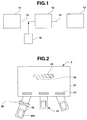
- Fig. 1 is a schematic block diagram showing the configuration of a first embodiment of the present invention.
- an MBE system 1 comprises a plurality of chambers including at least a chamber 11, a first chamber 12, and a second chamber 13.
- the chamber 11 is used to epitaxially grow III-V column compound semiconductor layers such as GaAs.
- the first chamber 12 is used to epitaxially grow II-V column compound semiconductor layers not containing Te, such as ZnSe, ZnMgSSe, ZnSSe, and ZnCdSe.
- the second chamber 13 is employed to epitaxially grow II-V column compound semiconductor layers containing at least Te such as ZnTe.
- the first chamber 12 is placed in the center.
- the chamber 11 and the second chamber 13 are connected to the first chamber.
- a chamber 16 for introducing a substrate is connected to an interconnection path 14 between the chamber 11 and the first chamber 12.
- gate valves (not shown) are mounted respectively in the interconnection path 14 and in an interconnection path 15 between the first chamber 12 and the second chamber 13 to hermetically isolate the chambers from each other.
- III-V column compound semiconductor layers are formed in their dedicated chamber 11.
- II-V column compound semiconductor layers not containing Te are formed in their dedicated first chamber 12.
- Compound semiconductor layers containing at least Te are formed in their dedicated second chamber 13. Therefore, Te is prevented from being mixed into the III-V column compound semiconductor layers or into the II-V column compound semiconductor layers not containing Te. Consequently, II-V column compound semiconductor layers which do not contain Te and have p-type and n-type layers of improved crystallinity can be formed.
- II-V column compound semiconductor layers having p-type ohmic characteristics can be formed.
- an optical semiconductor device having lower operation current, lower oscillation current, and higher emission intensity (i.e., having improved fundamental emission characteristics) compared with the prior art device can be realized.
- a substrate 110 of GaAs is supplied from the substrate-introducing chamber 16 into the chamber 11.
- the substrate 110 is heat-treated in the chamber 11.
- a buffer layer 121 of GaAs is epitaxially grown on the substrate 110.
- the buffer layer 121 is formed to a film thickness of about 0.3 ⁇ m, for example.
- the substrate 110 is moved into the first chamber 12 via the interconnection path 14. Thereafter, the II-V column compound semiconductor layers 120 not containing Te (i.e., from a buffer layer 122 to a p-type cladding layer 128) are epitaxially grown within the first chamber 12.
- the buffer layer 122 of ZnSe, an n-type cladding layer 123 of ZnMgSSe, an n-type guiding layer 124 of ZnSSe, an active layer 125 of ZnCdSe, a p-type guiding layer 126 of ZnSSe, a p-type cladding layer 127 of ZnMgSSe, and the p-type layer 128 of ZnSSe are successively epitaxially grown over the buffer layer 121.
- the film thickness of the buffer layer 122 is about 200 ⁇ .
- the film thickness of the n-type cladding layer 123 is about 0.8 ⁇ m.
- the film thickness of the n-type guiding layer 124 is about 600 ⁇ .
- the film thickness of the active layer 125 is about 60 ⁇ .
- the film thickness of the p-type guiding layer 126 is about 600 ⁇ .
- the film thicknesses of the p-type cladding layer 127 and p-type layer 128 are about 0.6 ⁇ m.
- n-type cladding layer 123 and of the n-type guiding layer 124 are doped with chlorine (Cl), for example.
- Cl chlorine
- N nitrogen
- the substrate 110 is moved into the second chamber 13 through the interconnection path 15.
- the contact layer 129 consisting of a multilayer film of ZnSe/ZnTe and the cap layer 130 of ZnTe are successively grown.
- the contact layer 129 is formed to a film thickness of about 150 ⁇ , for example.
- the cap layer 130 is grown to a film thickness of about 700 ⁇ .
- the contact layer 129 containing Te and the cap layer 130 are formed in the second chamber 13 which is used only for formation of II-V column compound semiconductor layers containing at least Te.
- the II-V column compound semiconductor layers 120 excluding the contact layer 129 and the cap layer 130 can be formed without mixing Te into those layers.
- the p-type cladding layer 127 and p-type layer 128 have hole concentrations not decreased and improved crystallinity.
- the n-type cladding layer 123 has good crystallinity.
- the contact layer 129 and the cap layer 130 formed in the second chamber 13 can be formed so as to contain Te and so p-type ohmic characteristics can be obtained.
- a semiconductor device whose fundamental light emission characteristics such as operation current, threshold current, and emission intensity are improved and which has improved life characteristics can be fabricated.
- FIG. 2 A second embodiment of the present invention is next described by referring to the schematic view of Fig. 2.
- this MBE system 2 has a chamber 21 used for fabrication of a II-V column compound semiconductor.
- a plurality of cells 24 are connected to the chamber.
- a holder 22 for holding a substrate 30 is mounted inside the chamber 21.
- Shutters 23 which can be opened and closed are mounted between their respective cells 24 and the holder 22.
- the plural cells 24 are provided for epitaxially grown constituent elements, respectively. These cells 24 include at least one cell 24a (hereinafter referred to as the cell used only for Te) for evaporating Te. A constituent element put in a crucible 25, for example, is supplied into each cell 24.
- a gate valve 26 which is a feature of the present invention is mounted in the cell 24a used only for Te and located on the side of the chamber 21.
- a chamber (not shown) for formation of III-V column compound semiconductors is connected with the chamber 21 used for formation of II-V column compound semiconductors.
- the gate valve 26 When the gate valve 26 is opened, the ambient inside the cell 24a used only for Te is placed in communication with the ambient inside the chamber 21. Therefore, when the gate valve 26 is opened, Te supplied into the cell 24a used only for Te enters the chamber 21. At this time, if the substrate 30 is held in the holder 22, a beam of Te reaches the surface of the substrate 30. Also, when the gate valve 26 is open, the crucible 25 supplied into the cell 24a used only for Te can be moved into that portion of the cell 24a used only for Te which is located on the side of the chamber 21.
- Te is prevented from being mixed into II-V column compound semiconductor layers not containing Te when they are formed. Also, p-type ohmic characteristics consisting of II-V column compound semiconductor layers containing Te can be formed.
- II-V column compound semiconductor layers which have p-type and n-type layers of improved crystallinity and which contain no Te can be formed. Therefore, an optical semiconductor device whose fundamental light emission characteristics have been improved and which has improved life characteristics can be fabricated.
- optical semiconductor device fabrication method using the above-described MBE system 2 is employed to fabricate a semiconductor laser emitting blue-green light as the optical semiconductor device described in connection with Fig. 3.
- a substrate 110 of GaAs is supplied into a chamber used for formation of III-V column compound semiconductors.
- the substrate 110 is heat-treated in this chamber.
- a buffer layer 121 of GaAs is epitaxially grown on the substrate 110.
- the substrate 110 is moved into the chamber 21 which is used for formation of II-V column compound semiconductors.
- the gate valve 26 mounted in the cell 24a used only for Te is closed.
- Te supplied into the cell 24a used only for Te is isolated.
- the II-V column compound semiconductor layers 120 are epitaxially grown from the buffer layer 122 not containing Te to the p-type cladding layer 128 in the chamber 21.
- the gate valve 26 is opened. Also, the crucible 25 holding Te is moved into a position close to the positions of the other crucibles 25 supplied into the other cells 24.
- the contact layer 129 consisting of a multilayer film of ZnSe/ZnTe and the cap layer 130 of ZnTe are successively epitaxially grown on the p-type layer 128.
- the II-V column compound semiconductor layers 120 are epitaxially grown from the buffer layer 122 not containing Te to the p-type layer 128.
- these layers can be formed from the buffer layer 122 to the p-type layer 128 without mixing Te into them.
- the p-type cladding layer 127, p-type layer 128 and n-type cladding layer 123 having improved crystallinity are obtained.
- the contact layer 129 and the cap layer 130 are formed.
- the contact layer 129 and the cap layer 130 are grown so as to contain Te.
- these layers 129 and 130 have p-type ohmic characteristics.
- an optical semiconductor device whose fundamental light emission characteristics have been improved and which has improved life characteristics can be fabricated.
- a semiconductor laser has been described as an example of optical semiconductor device. It is to be noted that the invention is not limited to this.
- a second chamber used only for formation of compound semiconductor layers containing at least Te is provided independent of a first chamber. Therefore, III-V column compound semiconductor layers and II-V column compound semiconductor layers not containing Te can be formed without mixing Te into them. Consequently, II-V column compound semiconductor layers having p-type layers whose hole concentration is prevented from decreasing and which have improved crystallinity can be formed, the II-V column compound semiconductor layers containing no Te. Furthermore, in the second chamber, II-V column compound semiconductor layers having p-type ohmic characteristics can be formed.
- a gate valve is mounted in a cell for evaporating Te and located on the side of the chamber, unlike other cells. Therefore, II-V column compound semiconductor layers not containing Te can be formed without mixing Te into them by opening and closing the gate valve. Alternatively, II-V column compound semiconductor layers containing Te can be formed.
- II-V column compound semiconductor layers containing Te can be formed without mixing Te into other layers. Therefore, an optical semiconductor device in which the hole concentrations of the other p-type layers not containing Te are prevented from decreasing and in which the crystallinity of n-type layers are not deteriorated can be manufactured.
- an optical semiconductor device having lower operation current, lower threshold current, higher emission intensity, and improved life characteristics compared with the prior art device can be realized.
Landscapes
- Chemical & Material Sciences (AREA)
- Engineering & Computer Science (AREA)
- Crystallography & Structural Chemistry (AREA)
- Materials Engineering (AREA)
- Metallurgy (AREA)
- Organic Chemistry (AREA)
- Inorganic Chemistry (AREA)
- Physical Deposition Of Substances That Are Components Of Semiconductor Devices (AREA)
- Semiconductor Lasers (AREA)
- Led Devices (AREA)
Abstract
Description
- The present invention relates to a molecular beam epitaxy (MBE) system capable of forming II-VI column compound semiconductor layers and also to a method of fabricating an optical semiconductor device, using this MBE system.
- II-V column compound semiconductors consisting of zinc selenide (ZnSe) or the like are applied to optical semiconductor devices such as laser diodes emitting blue-green light and light-emitting diodes.
- Where a semiconductor device is fabricated, using these II-V column compound semiconductors, the issue of ohmic contacts to p-type layer is still a subject, because it is difficult to obtain a high acceptor concentration. On the other hand, high p-type conductivity is obtained from zinc tellurium (ZnTe) more easily than from various other II-V column compound semiconductors. Consequently, the use of ZnTe is essential for formation of the above-described ohmic contact.
- An example of the optical semiconductor device which uses an ohmic contact made of ZnTe layer and emits blue-green light is shown in Fig. 3. This optical semiconductor device, 100, is a semiconductor laser. For example, this device uses a
substrate 110 made from gallium arsenide (GaAs). A buffer layer of GaAs 121 is formed on thesubstrate 110. II-V columncompound semiconductor layers 120 are formed on thebuffer layer 121. One example of this is described below. - Specifically, a
buffer layer 122 of ZnSe and an n-type cladding layer 123 consisting, for example, of zinc magnesium sulfur selenide (ZnMgSSe) are successively formed over theGaAs buffer layer 121. Furthermore, an n-type guidinglayer 124 made from zinc sulfur selenide (ZnSSe), anactive layer 125 consisting, for example, of zinc cadmium selenide (ZnCdSe), and a p-type guidinglayer 126 consisting of ZnSSe are stacked. - A p-
type cladding layer 127 made from zinc magnesium sulfur selenide (ZnMgSSe:N) and a p-type layer 128 made from ZnSSe are successively formed over the p-type guidinglayer 126. - A
contact layer 129 consisting, for example, of a multilayer film of ZnSe/ZnTe and having a superlattice structure and acap layer 130 made from ZnTe are successively formed over the p-type layer 128. That is, thecontact layer 129 and thecap layer 130 cooperate to form a p-type ohmic layer. Thus, the II-V columncompound semiconductor layers 120 are constituted. - Heretofore, the above-described II-V column
compound semiconductor layers 120 have been formed by MBE (molecular beam epitaxy) using an MBE system, for example. In the MBE process, the constituent elements of the II-V columncompound semiconductor layers 120 are evaporated in an ultra-high vacuum and epitaxially grown on thesubstrate 110, thus forming the layers 121-130. - However, tellurium (Te) is an element having a high vapor pressure and thus stagnant in nature. Therefore, where the substrate placed inside the chamber of the MBE system is isolated by a shutter from a Te cell connected with the chamber, if the temperature of the Te cell is elevated to a level at which growth is possible, then Te goes to the substrate through an unstraight route. For this reason, when the p-type cladding layer under the contact layer containing ZnTe is grown, Te is mixed into the p-type cladding layer. As a result, the hole concentration in the p-type cladding layer decreases. In consequence, the crystallinity deteriorates.
- For example, when the hole concentration in the p-type cladding layer consisting of ZnMgSSe is about 3 × 10¹⁷ cm⁻³, if about 2% Te is mixed into the selenium (Se) in the p-type cladding layer, then the hole concentration drops to about 1 × 10¹⁷ cm⁻³. Also, recombination center due to Te in the n-type cladding layer is observed with photoluminescence (PL) at 77 K.
- As a result, the fundamental emission characteristics are affected severely. For instance, the operation current or the threshold current of the formed optical semiconductor device increases, and the intensity of the emitted light decreases.
- It is an object of the invention to provide an MBE (molecular beam epitaxy) system and optical semiconductor device fabrication method capable of forming II-V column compound semiconductor layers having a p-type layer for the ohmic contact without mixing Te into other layers.
- The above-described object is achieved by an MBE system according to the present invention, the MBE system comprising a plurality of chambers including at least a first chamber and a second chamber. The first chamber is used to form II-V column compound semiconductor layers not containing Te. The second chamber is employed to form II-V column compound semiconductor layers containing at least Te.
- Another MBE system according to the invention has a chamber to which a plurality of cells are connected. The cells contain at least one cell for evaporating Te. In this system, a gate valve or gate valves are mounted in the cell or cells for evaporating the Te and located on the side of the chamber.
- A method of fabricating an optical semiconductor device according to the invention is a method of fabricating an optical semiconductor device by stacking II-V column compound semiconductor layers. II-V column compound semiconductor layers containing at least Te are formed, using any one of the MBE systems described above.
- The MBE system forming a first embodiment of the invention comprises a first chamber for forming II-V column compound semiconductor layers not containing Te and a second chamber for forming II-V column compound semiconductor layers containing at least Te. Therefore, the II-V column compound semiconductor layers not containing Te and the II-V column compound semiconductor layers containing Te are formed in their respective chambers. Consequently, Te is not mixed into the II-V column compound semiconductor layers not containing Te.
- In another embodiment of the invention, a gate valve or gate valves are mounted in the cell or cells for evaporating Te and located on the side of a chamber. Therefore, if the gate valve is closed, the ambient in the cell or cells is completely isolated from the ambient inside the chamber. As a result, when the gate valve is closed, Te supplied into the cell or cells is completely confined in the cells and does not enter the chamber. When the gate valve is opened, the ambient in the cell or cells is placed in communication with the ambient inside the chamber. Consequently, when the compound semiconductor layers not containing Te are formed, Te is not mixed into these layers.
- In a further embodiment of the invention, II-V column compound semiconductor layers containing Te are formed by using any one of the MBE systems described above without mixing Te into the other layers not containing Te.
-
- Fig. 1 is a block diagram of an MBE system forming a first embodiment of the invention;
- Fig. 2 is a side elevation partially in cross section of an MBE system forming a second embodiment of the invention; and
- Fig. 3 is a cross-sectional view of an optical semiconductor device fabricated, using an MBE system forming a third embodiment of the invention.
- The preferred embodiments of the present invention are hereinafter described in detail with reference to the accompanying drawings.
- Fig. 1 is a schematic block diagram showing the configuration of a first embodiment of the present invention. As shown, an MBE system 1 comprises a plurality of chambers including at least a
chamber 11, afirst chamber 12, and asecond chamber 13. - The
chamber 11 is used to epitaxially grow III-V column compound semiconductor layers such as GaAs. Thefirst chamber 12 is used to epitaxially grow II-V column compound semiconductor layers not containing Te, such as ZnSe, ZnMgSSe, ZnSSe, and ZnCdSe. Thesecond chamber 13 is employed to epitaxially grow II-V column compound semiconductor layers containing at least Te such as ZnTe. - In this example, the
first chamber 12 is placed in the center. Thechamber 11 and thesecond chamber 13 are connected to the first chamber. Achamber 16 for introducing a substrate is connected to aninterconnection path 14 between thechamber 11 and thefirst chamber 12. For example, gate valves (not shown) are mounted respectively in theinterconnection path 14 and in aninterconnection path 15 between thefirst chamber 12 and thesecond chamber 13 to hermetically isolate the chambers from each other. - In the above-described MBE system 1, III-V column compound semiconductor layers are formed in their
dedicated chamber 11. II-V column compound semiconductor layers not containing Te are formed in their dedicatedfirst chamber 12. Compound semiconductor layers containing at least Te are formed in their dedicatedsecond chamber 13. Therefore, Te is prevented from being mixed into the III-V column compound semiconductor layers or into the II-V column compound semiconductor layers not containing Te. Consequently, II-V column compound semiconductor layers which do not contain Te and have p-type and n-type layers of improved crystallinity can be formed. - Moreover, in the
second chamber 13, II-V column compound semiconductor layers having p-type ohmic characteristics can be formed. - Accordingly, if the MBE system 1 is used, an optical semiconductor device having lower operation current, lower oscillation current, and higher emission intensity (i.e., having improved fundamental emission characteristics) compared with the prior art device can be realized.
- The case in which the present optical semiconductor device fabrication method uses the above-described MBE system 1 is now described as an example. In this case, the semiconductor laser emitting blue-green light as already described in connection with Fig. 3 is fabricated as the optical semiconductor device.
- First, a
substrate 110 of GaAs is supplied from the substrate-introducingchamber 16 into thechamber 11. Thesubstrate 110 is heat-treated in thechamber 11. Then, abuffer layer 121 of GaAs is epitaxially grown on thesubstrate 110. At this time, thebuffer layer 121 is formed to a film thickness of about 0.3 µm, for example. - Then, the
substrate 110 is moved into thefirst chamber 12 via theinterconnection path 14. Thereafter, the II-V column compound semiconductor layers 120 not containing Te (i.e., from abuffer layer 122 to a p-type cladding layer 128) are epitaxially grown within thefirst chamber 12. - More specifically, the
buffer layer 122 of ZnSe, an n-type cladding layer 123 of ZnMgSSe, an n-type guiding layer 124 of ZnSSe, anactive layer 125 of ZnCdSe, a p-type guiding layer 126 of ZnSSe, a p-type cladding layer 127 of ZnMgSSe, and the p-type layer 128 of ZnSSe are successively epitaxially grown over thebuffer layer 121. - At this time, these layers 122-128 are so grown that the following film thicknesses are obtained. The film thickness of the
buffer layer 122 is about 200 Å. The film thickness of the n-type cladding layer 123 is about 0.8 µm. The film thickness of the n-type guiding layer 124 is about 600 Å. The film thickness of theactive layer 125 is about 60 Å. The film thickness of the p-type guiding layer 126 is about 600 Å. The film thicknesses of the p-type cladding layer 127 and p-type layer 128 are about 0.6 µm. Simultaneously with epitaxial growth of the n-type cladding layer 123 and of the n-type guiding layer 124, they are doped with chlorine (Cl), for example. Also, simultaneously with epitaxial growth of the p-type guiding layer 126 and of the p-type cladding layer 127 and p-type layer 128, they are doped with nitrogen (N), for example. - Then, the
substrate 110 is moved into thesecond chamber 13 through theinterconnection path 15. In thesecond chamber 12, thecontact layer 129 consisting of a multilayer film of ZnSe/ZnTe and thecap layer 130 of ZnTe are successively grown. At this time, thecontact layer 129 is formed to a film thickness of about 150 Å, for example. Thecap layer 130 is grown to a film thickness of about 700 Å. - In this method, the
contact layer 129 containing Te and thecap layer 130 are formed in thesecond chamber 13 which is used only for formation of II-V column compound semiconductor layers containing at least Te. For this reason, the II-V column compound semiconductor layers 120 excluding thecontact layer 129 and thecap layer 130 can be formed without mixing Te into those layers. As a result, the p-type cladding layer 127 and p-type layer 128 have hole concentrations not decreased and improved crystallinity. Also, the n-type cladding layer 123 has good crystallinity. - Furthermore, the
contact layer 129 and thecap layer 130 formed in thesecond chamber 13 can be formed so as to contain Te and so p-type ohmic characteristics can be obtained. - Accordingly, in the above example, a semiconductor device whose fundamental light emission characteristics such as operation current, threshold current, and emission intensity are improved and which has improved life characteristics can be fabricated.
- A second embodiment of the present invention is next described by referring to the schematic view of Fig. 2. As shown, this
MBE system 2 has achamber 21 used for fabrication of a II-V column compound semiconductor. A plurality ofcells 24 are connected to the chamber. Aholder 22 for holding asubstrate 30 is mounted inside thechamber 21.Shutters 23 which can be opened and closed are mounted between theirrespective cells 24 and theholder 22. - The
plural cells 24 are provided for epitaxially grown constituent elements, respectively. Thesecells 24 include at least onecell 24a (hereinafter referred to as the cell used only for Te) for evaporating Te. A constituent element put in acrucible 25, for example, is supplied into eachcell 24. - A
gate valve 26 which is a feature of the present invention is mounted in thecell 24a used only for Te and located on the side of thechamber 21. In this example, a chamber (not shown) for formation of III-V column compound semiconductors is connected with thechamber 21 used for formation of II-V column compound semiconductors. - In this
MBE system 2 constructed in this way, when thegate valve 26 is closed, the ambient inside thecell 24a used only for Te is completely isolated from the ambient inside thechamber 21. As a result, when thegate valve 26 is closed, Te supplied into thecell 24a used only for Te is completely confined within thecell 24a used only for Te. Therefore, the Te does not enter thechamber 21. - When the
gate valve 26 is opened, the ambient inside thecell 24a used only for Te is placed in communication with the ambient inside thechamber 21. Therefore, when thegate valve 26 is opened, Te supplied into thecell 24a used only for Te enters thechamber 21. At this time, if thesubstrate 30 is held in theholder 22, a beam of Te reaches the surface of thesubstrate 30. Also, when thegate valve 26 is open, thecrucible 25 supplied into thecell 24a used only for Te can be moved into that portion of thecell 24a used only for Te which is located on the side of thechamber 21. - Accordingly, in the
MBE system 2 of this example, Te is prevented from being mixed into II-V column compound semiconductor layers not containing Te when they are formed. Also, p-type ohmic characteristics consisting of II-V column compound semiconductor layers containing Te can be formed. - Consequently, II-V column compound semiconductor layers which have p-type and n-type layers of improved crystallinity and which contain no Te can be formed. Therefore, an optical semiconductor device whose fundamental light emission characteristics have been improved and which has improved life characteristics can be fabricated.
- A third embodiment is described now. In this embodiment, the optical semiconductor device fabrication method using the above-described
MBE system 2 is employed to fabricate a semiconductor laser emitting blue-green light as the optical semiconductor device described in connection with Fig. 3. - First, a
substrate 110 of GaAs is supplied into a chamber used for formation of III-V column compound semiconductors. Thesubstrate 110 is heat-treated in this chamber. Then, abuffer layer 121 of GaAs is epitaxially grown on thesubstrate 110. - Then, the
substrate 110 is moved into thechamber 21 which is used for formation of II-V column compound semiconductors. At this time, thegate valve 26 mounted in thecell 24a used only for Te is closed. As a result, Te supplied into thecell 24a used only for Te is isolated. Subsequently, the II-V column compound semiconductor layers 120 are epitaxially grown from thebuffer layer 122 not containing Te to the p-type cladding layer 128 in thechamber 21. - Immediately after the end of the growth of the p-
type layer 128, thegate valve 26 is opened. Also, thecrucible 25 holding Te is moved into a position close to the positions of theother crucibles 25 supplied into theother cells 24. Thecontact layer 129 consisting of a multilayer film of ZnSe/ZnTe and thecap layer 130 of ZnTe are successively epitaxially grown on the p-type layer 128. - In this method, when the
gate valve 26 which is mounted in thecell 24a used only for Te and located on the side of thechamber 21 is closed, the II-V column compound semiconductor layers 120 are epitaxially grown from thebuffer layer 122 not containing Te to the p-type layer 128. As a result, these layers can be formed from thebuffer layer 122 to the p-type layer 128 without mixing Te into them. In consequence, the p-type cladding layer 127, p-type layer 128 and n-type cladding layer 123 having improved crystallinity are obtained. - When the
gate valve 26 is open, thecontact layer 129 and thecap layer 130 are formed. The result is that thecontact layer 129 and thecap layer 130 are grown so as to contain Te. Hence, theselayers - Accordingly, in the above example, an optical semiconductor device whose fundamental light emission characteristics have been improved and which has improved life characteristics can be fabricated. In the example described above, a semiconductor laser has been described as an example of optical semiconductor device. It is to be noted that the invention is not limited to this.
- As described thus far, in the first embodiment of the invention, a second chamber used only for formation of compound semiconductor layers containing at least Te is provided independent of a first chamber. Therefore, III-V column compound semiconductor layers and II-V column compound semiconductor layers not containing Te can be formed without mixing Te into them. Consequently, II-V column compound semiconductor layers having p-type layers whose hole concentration is prevented from decreasing and which have improved crystallinity can be formed, the II-V column compound semiconductor layers containing no Te. Furthermore, in the second chamber, II-V column compound semiconductor layers having p-type ohmic characteristics can be formed.
- In the second embodiment of the invention, a gate valve is mounted in a cell for evaporating Te and located on the side of the chamber, unlike other cells. Therefore, II-V column compound semiconductor layers not containing Te can be formed without mixing Te into them by opening and closing the gate valve. Alternatively, II-V column compound semiconductor layers containing Te can be formed.
- In the third embodiment of the invention, II-V column compound semiconductor layers containing Te can be formed without mixing Te into other layers. Therefore, an optical semiconductor device in which the hole concentrations of the other p-type layers not containing Te are prevented from decreasing and in which the crystallinity of n-type layers are not deteriorated can be manufactured.
- Accordingly, an optical semiconductor device having lower operation current, lower threshold current, higher emission intensity, and improved life characteristics compared with the prior art device can be realized.
Claims (7)
- A molecular beam epitaxy system comprising:
a first chamber for forming layers of semiconductors of II-V column compounds not containing tellurium; and
a second chamber for forming layers of semiconductors of II-V column compounds containing at least tellurium. - A molecular beam epitaxy system having a chamber to which a plurality of cells are connected, said cells containing at least one cell for evaporating tellurium, said system comprising:
a gate valve mounted in said cell for evaporating tellurium and located on a side of said chamber. - A molecular beam epitaxy system comprising:
a first chamber for forming layers of semiconductors of II-V column compounds not containing tellurium;
a second chamber for forming layers of semiconductors of II-V column compounds containing at least tellurium;
a plurality of cells connected to said second chamber; and
a gate valve mounted in said cell for evaporating tellurium and located on a side of said second chamber. - A method of fabricating an optical semiconductor device having laminated II-V column compound semiconductor layers, comprising the step of:
forming the II-V column compound semiconductor layers containing at least tellurium, using the system of claim 1 or 2. - A method of fabricating an optical semiconductor device as set forth in claim 4, wherein said II-V column compound semiconductor layers form a multilayer film of ZnSe and ZnTe.
- A method of fabricating an optical semiconductor device as set forth in claim 5, wherein said ZnSe and ZnTe form contact layers and said ZnTe forms a cap layer, and wherein said optical semiconductor device forms a laser emitting blue light.
- A method of fabricating an optical semiconductor device acting as a laser emitting blue light as set forth in claim 6, wherein II-V column compound semiconductor layers are formed from a buffer layer not containing Te to a cladding layer while closing said gate valve, and wherein said contact layer and said cap layer are formed while opening said gate valve.
Applications Claiming Priority (2)
| Application Number | Priority Date | Filing Date | Title |
|---|---|---|---|
| JP24693594A JPH0888175A (en) | 1994-09-14 | 1994-09-14 | Molecular beam epitaxial growth apparatus and optical semiconductor device manufacturing method |
| JP246935/94 | 1994-09-14 |
Publications (2)
| Publication Number | Publication Date |
|---|---|
| EP0702101A2 true EP0702101A2 (en) | 1996-03-20 |
| EP0702101A3 EP0702101A3 (en) | 1996-09-18 |
Family
ID=17155942
Family Applications (1)
| Application Number | Title | Priority Date | Filing Date |
|---|---|---|---|
| EP95114404A Withdrawn EP0702101A3 (en) | 1994-09-14 | 1995-09-13 | MBE system and semiconductor device manufactured using this system |
Country Status (6)
| Country | Link |
|---|---|
| US (1) | US5989339A (en) |
| EP (1) | EP0702101A3 (en) |
| JP (1) | JPH0888175A (en) |
| KR (1) | KR960012304A (en) |
| MY (1) | MY116369A (en) |
| SG (1) | SG49976A1 (en) |
Cited By (8)
| Publication number | Priority date | Publication date | Assignee | Title |
|---|---|---|---|---|
| WO1999003144A1 (en) * | 1997-07-08 | 1999-01-21 | Osram Opto Semiconductors Gmbh & Co. Ohg | Method for producing a ii-vi semi-conducting component |
| EP1054082A1 (en) * | 1999-05-21 | 2000-11-22 | Stanley Electric Co., Ltd. | P-type group II-VI compound semiconductor crystals, growth method for such crystals, and semiconductor device made of such crystals |
| WO2002064852A1 (en) * | 2001-02-09 | 2002-08-22 | Motorola, Inc. | Apparatus for fabricating semiconductor structures |
| WO2004070900A1 (en) * | 2003-01-27 | 2004-08-19 | Finisar Corporation | System and methods using migration enhanced epitaxy for flattening active layers and the mechanical stabilization of quantum wells associated with vertical cavity surface emitting lasers |
| US7167495B2 (en) | 1998-12-21 | 2007-01-23 | Finisar Corporation | Use of GaAs extended barrier layers between active regions containing nitrogen and AlGaAs confining layers |
| US7257143B2 (en) | 1998-12-21 | 2007-08-14 | Finisar Corporation | Multicomponent barrier layers in quantum well active regions to enhance confinement and speed |
| US7286585B2 (en) | 1998-12-21 | 2007-10-23 | Finisar Corporation | Low temperature grown layers with migration enhanced epitaxy adjacent to an InGaAsN(Sb) based active region |
| US7435660B2 (en) | 1998-12-21 | 2008-10-14 | Finisar Corporation | Migration enhanced epitaxy fabrication of active regions having quantum wells |
Families Citing this family (5)
| Publication number | Priority date | Publication date | Assignee | Title |
|---|---|---|---|---|
| KR100265592B1 (en) * | 1997-06-20 | 2000-11-01 | 김영환 | Internal address generator |
| DE19824222A1 (en) * | 1998-05-29 | 1999-12-02 | Lite On Electronics Inc | Transparent window layer for light emitting diode |
| US6368983B1 (en) * | 1999-04-09 | 2002-04-09 | Raytheon Company | Multi-layer wafer fabrication |
| GB2470190B (en) | 2009-05-11 | 2011-07-13 | Nexeon Ltd | A binder for lithium ion rechargeable battery cells |
| US9853292B2 (en) * | 2009-05-11 | 2017-12-26 | Nexeon Limited | Electrode composition for a secondary battery cell |
Family Cites Families (7)
| Publication number | Priority date | Publication date | Assignee | Title |
|---|---|---|---|---|
| US4681773A (en) * | 1981-03-27 | 1987-07-21 | American Telephone And Telegraph Company At&T Bell Laboratories | Apparatus for simultaneous molecular beam deposition on a plurality of substrates |
| JPS5895695A (en) * | 1981-11-30 | 1983-06-07 | Fujitsu Ltd | Crystal growing apparatus with molecular beam |
| JPS63148617A (en) * | 1986-12-12 | 1988-06-21 | Hitachi Ltd | Molecular beam epitaxy apparatus |
| JPH0647515B2 (en) * | 1988-12-08 | 1994-06-22 | シャープ株式会社 | Compound semiconductor epitaxial growth method |
| WO1994015369A1 (en) * | 1992-12-22 | 1994-07-07 | Research Corporation Technologies, Inc. | Group ii-vi compound semiconductor light emitting devices and an ohmic contact therefor |
| JP2772607B2 (en) * | 1993-03-18 | 1998-07-02 | 国際電信電話株式会社 | Method and apparatus for producing nitrogen-doped II-VI compound semiconductor thin film |
| US5492080A (en) * | 1993-12-27 | 1996-02-20 | Matsushita Electric Industrial Co., Ltd. | Crystal-growth method and semiconductor device production method using the crystal-growth method |
-
1994
- 1994-09-14 JP JP24693594A patent/JPH0888175A/en active Pending
-
1995
- 1995-09-08 SG SG1996010666A patent/SG49976A1/en unknown
- 1995-09-12 MY MYPI95002693A patent/MY116369A/en unknown
- 1995-09-12 KR KR1019950029598A patent/KR960012304A/en not_active Withdrawn
- 1995-09-13 EP EP95114404A patent/EP0702101A3/en not_active Withdrawn
- 1995-09-13 US US08/527,456 patent/US5989339A/en not_active Expired - Lifetime
Non-Patent Citations (1)
| Title |
|---|
| None |
Cited By (11)
| Publication number | Priority date | Publication date | Assignee | Title |
|---|---|---|---|---|
| WO1999003144A1 (en) * | 1997-07-08 | 1999-01-21 | Osram Opto Semiconductors Gmbh & Co. Ohg | Method for producing a ii-vi semi-conducting component |
| US6399473B1 (en) | 1997-07-08 | 2002-06-04 | Osram Opto Semiconductors Gmbh & Co. Ohg | Method of producing a II-VI semiconductor component containing selenium and/or sulrfur |
| US7167495B2 (en) | 1998-12-21 | 2007-01-23 | Finisar Corporation | Use of GaAs extended barrier layers between active regions containing nitrogen and AlGaAs confining layers |
| US7257143B2 (en) | 1998-12-21 | 2007-08-14 | Finisar Corporation | Multicomponent barrier layers in quantum well active regions to enhance confinement and speed |
| US7286585B2 (en) | 1998-12-21 | 2007-10-23 | Finisar Corporation | Low temperature grown layers with migration enhanced epitaxy adjacent to an InGaAsN(Sb) based active region |
| US7378680B2 (en) | 1998-12-21 | 2008-05-27 | Finisar Corporation | Migration enhanced epitaxy fabrication of quantum wells |
| US7435660B2 (en) | 1998-12-21 | 2008-10-14 | Finisar Corporation | Migration enhanced epitaxy fabrication of active regions having quantum wells |
| EP1054082A1 (en) * | 1999-05-21 | 2000-11-22 | Stanley Electric Co., Ltd. | P-type group II-VI compound semiconductor crystals, growth method for such crystals, and semiconductor device made of such crystals |
| US6407405B1 (en) | 1999-05-21 | 2002-06-18 | Stanley Electric Co., Ltd. | p-Type group II-VI compound semiconductor crystals growth method for such crystals, and semiconductor device made of such crystals |
| WO2002064852A1 (en) * | 2001-02-09 | 2002-08-22 | Motorola, Inc. | Apparatus for fabricating semiconductor structures |
| WO2004070900A1 (en) * | 2003-01-27 | 2004-08-19 | Finisar Corporation | System and methods using migration enhanced epitaxy for flattening active layers and the mechanical stabilization of quantum wells associated with vertical cavity surface emitting lasers |
Also Published As
| Publication number | Publication date |
|---|---|
| JPH0888175A (en) | 1996-04-02 |
| MY116369A (en) | 2004-01-31 |
| SG49976A1 (en) | 1998-06-15 |
| EP0702101A3 (en) | 1996-09-18 |
| US5989339A (en) | 1999-11-23 |
| KR960012304A (en) | 1996-04-20 |
Similar Documents
| Publication | Publication Date | Title |
|---|---|---|
| Ishibashi | II–VI blue-green light emitters | |
| US5751021A (en) | Semiconductor light-emitting device | |
| CN1321488C (en) | laser diode | |
| US5818072A (en) | Integrated heterostructure of group II-VI semiconductor materials including epitaxial ohmic contact and method of fabricating same | |
| US5646419A (en) | n-type wide bandgap semiconductors grown on a p-type layer to form hole injection pn heterojunctions and methods of fabricating the same | |
| US4639275A (en) | Forming disordered layer by controlled diffusion in heterojunction III-V semiconductor | |
| US5291507A (en) | Blue-green laser diode | |
| EP1189290A1 (en) | Semiconductor device having ZnO based oxide semiconductor layer and method of manufacturing the same | |
| US5989339A (en) | MBE system and semiconductor device fabricated, using same | |
| US5508522A (en) | Method for producing a group II-VI compound semiconductor thin film and a group II-VI compound semiconductor device | |
| US6090637A (en) | Fabrication of II-VI semiconductor device with BeTe buffer layer | |
| US7449720B2 (en) | Epitaxial wafer for semiconductor light-emitting devices, and semiconductor light-emitting device | |
| EP1016175B1 (en) | Be-CONTAINING II-VI BLUE-GREEN LASER DIODES | |
| US5872023A (en) | Method of fabricating of light emitting device with controlled lattice mismatch | |
| US6399473B1 (en) | Method of producing a II-VI semiconductor component containing selenium and/or sulrfur | |
| JP2586349B2 (en) | Semiconductor light emitting device | |
| US5377214A (en) | Tensile strained blue green II-VI quantum well Laser | |
| US5324963A (en) | Electroluminescent semiconductor device having chalcogenide layer and mixed crystal layer | |
| JP3333346B2 (en) | Semiconductor device | |
| KR20050024078A (en) | Method to Make Light Emitting Devices using p-ZnO | |
| JP3405552B2 (en) | Optical semiconductor device | |
| JPH08162481A (en) | Crystal growth method | |
| KR100459579B1 (en) | Be-containing ⅱ-ⅵ blue-green laser diodes | |
| Yakovlev et al. | Novel hybrid III-V/II-VI mid-infrared laser structures with high asymmetric band offset confinements | |
| JPH07193335A (en) | Ohmic electrode structure and light emitting device using the same |
Legal Events
| Date | Code | Title | Description |
|---|---|---|---|
| PUAI | Public reference made under article 153(3) epc to a published international application that has entered the european phase |
Free format text: ORIGINAL CODE: 0009012 |
|
| AK | Designated contracting states |
Kind code of ref document: A2 Designated state(s): DE FR GB |
|
| PUAL | Search report despatched |
Free format text: ORIGINAL CODE: 0009013 |
|
| RHK1 | Main classification (correction) |
Ipc: H01L 21/363 |
|
| AK | Designated contracting states |
Kind code of ref document: A3 Designated state(s): DE FR GB |
|
| 17P | Request for examination filed |
Effective date: 19970218 |
|
| 17Q | First examination report despatched |
Effective date: 20011213 |
|
| STAA | Information on the status of an ep patent application or granted ep patent |
Free format text: STATUS: THE APPLICATION IS DEEMED TO BE WITHDRAWN |
|
| 18D | Application deemed to be withdrawn |
Effective date: 20030401 |