EP0702290B1 - Dispositif de division numérique utilisant une table de consultation - Google Patents
Dispositif de division numérique utilisant une table de consultation Download PDFInfo
- Publication number
- EP0702290B1 EP0702290B1 EP95114315A EP95114315A EP0702290B1 EP 0702290 B1 EP0702290 B1 EP 0702290B1 EP 95114315 A EP95114315 A EP 95114315A EP 95114315 A EP95114315 A EP 95114315A EP 0702290 B1 EP0702290 B1 EP 0702290B1
- Authority
- EP
- European Patent Office
- Prior art keywords
- digital
- bit
- signal
- input signal
- bits
- Prior art date
- Legal status (The legal status is an assumption and is not a legal conclusion. Google has not performed a legal analysis and makes no representation as to the accuracy of the status listed.)
- Expired - Lifetime
Links
Images



Classifications
-
- G—PHYSICS
- G06—COMPUTING OR CALCULATING; COUNTING
- G06F—ELECTRIC DIGITAL DATA PROCESSING
- G06F7/00—Methods or arrangements for processing data by operating upon the order or content of the data handled
- G06F7/38—Methods or arrangements for performing computations using exclusively denominational number representation, e.g. using binary, ternary, decimal representation
- G06F7/48—Methods or arrangements for performing computations using exclusively denominational number representation, e.g. using binary, ternary, decimal representation using non-contact-making devices, e.g. tube, solid state device; using unspecified devices
- G06F7/52—Multiplying; Dividing
- G06F7/535—Dividing only
-
- G—PHYSICS
- G06—COMPUTING OR CALCULATING; COUNTING
- G06F—ELECTRIC DIGITAL DATA PROCESSING
- G06F1/00—Details not covered by groups G06F3/00 - G06F13/00 and G06F21/00
- G06F1/02—Digital function generators
- G06F1/03—Digital function generators working, at least partly, by table look-up
- G06F1/035—Reduction of table size
Definitions
- the present invention relates to a digital dividing apparatus using a look-up table, and more particularly, to an apparatus for calculating a ratio of one digital input signal to the sum of two digital input signals.
- signals like a video signal and an audio signal have been conventionally processed by an analog circuit in an analog manner.
- an analog signal processing technique is increasingly replaced with a technique of converting signals into a digital form and processing them in a digital manner.
- a digital signal processing circuit which performs such a signal processing as described above is often required to calculate a ratio of one input signal to the sum of two digital input signals.
- a dividing apparatus 52 including an adder 50 and a divider 51 as illustrated in Fig. 1, for example, is used.
- Adder 50 calculates the sum of input signals A and B
- divider 51 divides input signal B by the sum calculated by adder 50.
- dividing apparatus 52 outputs a value of B/(A+B).
- Such a dividing apparatus 52 needs to preform operation every time input signals A and B are supplied, and therefore, it requires a lot of time for operation, resulting in long delay time of signals passing through such a dividing apparatus 52.
- LUT look-up table
- This LUT is constituted by addresses corresponding to every possible value of each of input signals A and B and ratios of B/(A+B) calculated for each value of input signals A and B, and the LUT is pre-stored in an LUT memory.
- This LUT enables a ratio of B/(A+B) to be read from the memory in response to input signals A and B without actual calculation.
- the ratio of B/(A+B) calculated by dividing apparatus 52 of Fig. 1 is of course "1" or less. In digital calculation, however, decimal parts will not be used as they are.
- An output signal of dividing apparatus 52 is converted so that a prescribed value of the output signal indicates "1", and decimal parts of the output signal is rounded down.
- a digital dividing apparatus for calculating such a ratio as described above outputs digital quotient data C given by the following equation (1) where "int” indicates that decimal parts of a value in the subsequent parentheses are rounded down, and W represents the number of bits (bit width) of an output signal. When both input signals are "0", data C is 2 W-2 .
- a digital dividing apparatus responsive to a first M bit digital input signal A and a second N bit digital input signal B (where each of M and N is a positive integer) for producing a digital output signal for B/(A+B) includes a first multiplying circuit, a second multiplying circuit, a first round down circuit, a second round down circuit, a look-up table storage circuit, and a control circuit.
- the first multiplying circuit multiplies the first digital input signal A by 2 K where K is a positive integer.
- the second multiplying circuit multiplies the second digital input signal B by 2 K . K is determined so that said first and second multiplying circuit will not cause overflow of said input signals A and B, respectively.
- the first round down circuit rounds down at least one bit of a first digital product signal A x 2 K output from the first multiplying circuit and produces a first m bit digital round down signal ⁇ where m is a positive integer smaller than M.
- the second round down circuit rounds down at least one bit of a second digital product signal B x 2 K output from the second multiplying circuit and produces a second n bit digital round down signal ⁇ where n is a positive integer smaller than N.
- the look up table storage circuit pre-stores a look up table.
- the look up table includes 2 m+n digital quotient data for ⁇ /( ⁇ + ⁇ )corresponding to 2 m+n combinations of 2 m possible values of the first digital round down signal ⁇ and 2 n possible values of the second digital round down signal ⁇ .
- the control circuit is responsive to the first. digital round down signal ⁇ from the first round down circuit and the second digital round down signal ⁇ from the second round down circuit, and controls the look up table storage circuit so that corresponding one of 2 m+n digital quotient data is read as a digital output signal.
- this digital dividing apparatus includes the look up table storage circuit and calculates the ratio of B/(A+B) using a look up table stored therein, calculation speed thereof increases.
- This digital dividing apparatus further includes the first and the second round down circuits by which lower bits of the first and the second input signals A and B are rounded down, respectively, and therefore, a scale of the look up table storage circuit is reduced.
- the digital dividing apparatus further includes the first and the second multiplying circuits which multiplies the first and the second digital input signals A and B by 2 K before rounding down the first and the second digital input signals A and B, respectively, operation error thereof is reduced as a result.
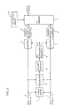
- Fig. 1 is a block diagram showing a conventional apparatus for calculating a ratio of B/(A+B).
- Fig. 2 is a block diagram showing the whole arrangement of a digital dividing apparatus in accordance with a first embodiment of the present invention.
- Fig. 3 is a diagram illustrating an operation of the digital dividing apparatus shown in Fig. 2.
- Fig. 4 is a block diagram showing the whole arrangement of a digital dividing apparatus in accordance with a second embodiment of the present invention.
- Fig. 5 is a diagram illustrating an operation specific to the digital dividing apparatus shown in Fig. 4.
- a digital dividing apparatus includes an input terminal 1 for one bus and an input terminal 2 for another bus.
- a 10 bit digital input signal A is supplied to input terminal 1
- another 10 bit digital input signal B is supplied to input terminal 2.
- the digital dividing apparatus further includes a comparator 3 for receiving input signals A and B and comparing input signal A with input signal B; a selector 4 responsive to an output from comparator 3 for selecting a larger input signal out of input signals A and B; a priority encoder 5 for receiving the input signal selected by selector 4 and outputting a digital priority signal in which only a bit corresponding to the most significant bit out of bits indicating "1" of the selected input signal indicates "1'; a bit difference encoder 6 responsive to the digital priority signal output from priority encoder 5 for outputting a bit difference K between the most significant bit (MSB) of the selected input signal and the most significant bit out of bits indicating "1" of the selected input signal; a shifter 7 for shifting each bit of input signal A to the upper side thereof by the bit different K;
- the LUT further includes 256 8-bit digital quotient data C for ⁇ /( ⁇ + ⁇ )corresponding to 256 addresses.
- LUT memory 11 is controlled by LUT control circuit 12, whereby one of 256 digital quotient data C described above is read as a digital output signal.
- Digital quotient data C for ⁇ /( ⁇ + ⁇ ) is calculated with the following equation (2) for every possible value of each of digital round down signals ⁇ and ⁇ , and each of the calculated data C is pre-stored in a corresponding address.
- a and B are simply replaced with ⁇ and ⁇ , respectively, since the digital dividing apparatus converts input signals A and B into round down signals ⁇ and ⁇ , respectively, and calculates the ratio of ⁇ /( ⁇ + ⁇ )based on the converted round down signals ⁇ and ⁇ .
- FIG. 3(a) is a 10 bit digital input signal A having a value of "31”.
- Fig. 3(b) is a 10 bit digital input signal B having a value of "15”.
- Comparator 3 compares input signal A with input signal B, and determines which input signal is larger. In this case, since input signal A is larger than input signal B, comparator 3 supplies selector 4 with the result showing input signal A is larger than input signal B. Selector 4 receives the result, the selects the larger input signal A as shown in Fig. 3(c) for supply to priority encoder 5.
- Priority encoder 5 produces a priority signal as shown in Fig. 3(d) in response to the input signal supplied from selector 4.
- the priority signal has 10 bits as input signals A and B. One bit out of 10 bits in the priority signal indicates “1". This bit indicating "1" corresponds to the most significant bit out of bits indicating "1" of input signal A supplied from selector 4. In this case, since upper 5 bits of input signal A are “0" and lower 5 bits thereof are “1", the sixth bit from the most significant bit (MSB) of input signal A is most significant out of bits indicating "1". Accordingly, as shown in Fig. 3(d), only the sixth bit from the most significant bit of the priority signal indicates "1". Such a priority signal is supplied to bit difference encoder 6.
- Bit difference K 0, 1, 2, ..., 9 from the most significant bit is shown under the 10 bit priority signal of Fig. 3(d).
- the sixth bit from the most significant bit indicates “1", and therefore, the bit difference K between the most significant bit (MSB) and the most significant bit out of bits indicating "1" in input signal A is "5".
- bit difference encoder 6 converts the bit difference K into a 4 bit signal, a 4 bit digital signal indicating the bit difference K of "5" as shown in Fig. 3(e) is supplied to each of shifters 7 and 8.
- Shifter 7 once holds the 10 bit input signal A, and then, shifts each bit of the held 10 bit input signal A to the upper side by the bit difference K supplied from bit difference encoder 6.
- input signal A as shown in Fig. 3(a) is shifted to the upper side by 5 bits, and therefore, a 10 bit signal as shown in Fig. 3(f) is supplied to round down circuit 9.
- Shifter 8 once holds the 10 bit input signal B, and then, shifts each bit of the held input signal B to the upper side by the bit difference K supplied from bit difference encoder 6.
- input signal B as shown in Fig. 3(b) is shifted to the upper side by 5 bits, and therefore, a 10 bit signal as shown in Fig. 5(g) is supplied to round down circuit 10.
- shifter 7 multiplies input signal A by 2 K
- shifter 8 multiples input signal B by 2 K .
- input signal B of "15” is multiplied by 32.
- comparator 3, selector 4, priority encoder 5, and bit difference encoder 6 determine the bit difference K so that shifters 7 and 8 will not cause overflow of input signals A and B, respectively.
- the bit difference K determined is the maximum within the range which does not cause overflow of input signals A and B.
- Input signals A and B each shifted to the side of upper bits within the range which does not cause overflow thereof are applied to round down circuits 9 and 10, respectively.
- Round down circuit 9 rounds down lower 6 bits of the shifted input signal A. Therefore, a 4 bit digital round down signal ⁇ as shown in Fig. 3(h) is applied from round down circuit 9 to LUT memory 11.
- round down circuit 10 rounds down lower 6 bits of the shifted input signal B. Therefore, a 4 bit digital round down signal ⁇ as shown in Fig. 3(i) is applied from round down circuit 10 to LUT memory 11. In this case, round down signal ⁇ is "15" and round down signal ⁇ is "7".
- LUT control circuit 12 applies round down signals ⁇ and ⁇ to LUT memory 11 as an address, and reads digital quotient data C based on the applied address.
- This read quotient data C is output from LUT memory 11 as an 8 bit output signal.
- "15" is applied to LUT memory 11 as round down signal ⁇
- "7" is applied to LUT memory 11 as round down signal ⁇
- LUT control circuit 12 accesses an address as shown in Fig. 3(j).
- digital quotient data indicating "40" as shown in Fig. 3(k) is read from LUT memory 11 as a digital output signal.
- LUT memory 11 requires 2 20 byte capacity.
- LUT memory 11 is provided with addresses of 10 bit input signals A and B, and digital quotient data C calculated according to the equation (1) would be pre-stored in respective addresses. Accordingly, if input signal A of "31" and input signal B of "15" are applied to the LUT memory, for example, data C of "41" would be read as an output signal.
- an output signal calculated by the present embodiment has an error of only "1". This is because shifters 7 and 8 shift input signals A and B to the upper side of bits as much as possible within the range which does not cause overflow, respectively.
- This table shows errors calculated based on a value obtained when 10 bit input signals A and B are applied directly to the LUT memory and an 8 bit output signal is read from the LUT memory. More specifically, a value of each of input signals A and B was varied sequentially from “0" through “1023”, and quotient data C for every possible value of each of input signals A and B were calculated according to the equation (1). Corresponding quotient data C were also calculated by the above-described simple round down method. Furthermore, corresponding quotient data were also calculated by the present embodiment. Then, errors were calculated for every possible value of each of input signals A and B, based on the quotient data obtained as described above. The above table shows the maximum error obtained by the simple round down method and the maximum error obtained by the present embodiment.
- each error obtained by each of the simple round down method and the present embodiment was squared, and mean square error was calculated for each of the simple round down method and the present embodiment.
- the present embodiment can suppress the error extremely small compared to the simple round down method.
- bit width supplementing circuit 30 is added to the side of an input terminal 2.
- a 10 bit input signal A is supplied to an input terminal 1
- an 8 bit input signal B is supplied to input terminal 2.
- Bit width supplementing circuit 30 is provided only on the side to which input signal B having smaller number of bits is supplied. Accordingly, 8 bit input signal B is applied to bit width supplementing circuit 30 before being applied to a shifter 8.
- 2 bits indicating "0" are added to the upper side of bits of the applied 8 bit input signal B.
- bit width supplementing circuit 30 If 8 bit input signal B of "15" as shown in Fig. 5(b) is applied to bit width supplementing circuit 30, for example, 2 bits are added to the upper side of bits of the applied input signal B as shown in Fig. 5(c). These added 2 bits are set to "0". Therefore, 8 bit input signal B is converted into a 10 bit signal by bit width supplementing circuit 30 without change of the value.
- An output signal of bit width supplementing circuit 30 shown in Fig. 5(c) is the same as the signal shown in Fig. 3(b). Accordingly, subsequent operation of the second embodiment is similar to the operation of the above-mentioned first. embodiment shown in Fig. 2.
- round down circuits 9 and 10 are not limited to 6, and round down circuits 9 and 10 may be constituted to round down lower 7 bits of an input signal, for example.
- round down circuits 9 and 10 are constituted to round down lower 5 bits of an input signal, capacity required for the LUT memory is increased, whereas an error produced in an output signal of LUT memory 11 is reduced.
- round down circuits 9 and 10 round down the same number of bits in the first and the second embodiments, they may round down different number of bits from each other.
- round down circuit 9 may round down lower 6 bits of an input signal A
- round down circuit 10 may round down lower 5 bits of an input signal B.
- a 4 bit round down signal is applied from round down circuit 9 to LUT memory 11
- a 5 bit round down signal is applied form round down circuit 10 to LUT memory 11, and therefore, an LUT corresponding to such round down signals must be pre-stored in LUT memory 11. More specifically, quotient data for every possible value of each of the 4 bit round down signal and the 5 bit round down signal must be precalculated.
- a round down signal ⁇ is applied as an upper address of LUT memory 11 and a 4 bit round down signal ⁇ is applied as a lower address of LUT memory 11 in the first and the second embodiments, a round down signal ⁇ may be applied as a lower address and a round down signal ⁇ may be applied as an upper address.
- a bit width supplementing circuit may be added to the side of an input terminal 1 to which an input signal A is supplied if the number of bits of input signal A is smaller than that of input signal B.
Landscapes
- Engineering & Computer Science (AREA)
- Theoretical Computer Science (AREA)
- General Physics & Mathematics (AREA)
- Physics & Mathematics (AREA)
- Mathematical Analysis (AREA)
- Mathematical Optimization (AREA)
- Pure & Applied Mathematics (AREA)
- Computational Mathematics (AREA)
- General Engineering & Computer Science (AREA)
- Computing Systems (AREA)
- Complex Calculations (AREA)
- Analogue/Digital Conversion (AREA)
- Compression, Expansion, Code Conversion, And Decoders (AREA)
Claims (9)
- Dispositif de division numérique pour un premier signal numérique d'entrée A de M bits et un second signal numérique d'entrée B de N bits, dont M et N sont chacun un nombre entier positif, pour produire un signal numérique de sortie de B/(A+B), comprenant:un premier moyen multiplicateur (7) pour multiplier ledit premier signal numérique d'entrée A par 2K;un second moyen multiplicateur (8) pour multiplier ledit second signal numérique d'entrée B par 2K, où K représente un nombre entier positif déterminé de manière à ce que lesdits premier et second moyens multiplicateur (7, 8) ne provoquent pas de dépassement des signaux d'entrée respectifs A et B;un premier moyen d'arrondissement au chiffre inférieur (9) pour arrondir au chiffre inférieur au moins un bit inférieur prédéterminé d'un premier signal numérique de produit A x 2K fourni en sortie dudit premier moyen multiplicateur afin de produire un premier signal numérique α de m bits arrondi au chiffre inférieur, où m est un nombre entier positif inférieur à M;un second moyen d'arrondissement au chiffre inférieur (10) pour arrondir au chiffre inférieur au moins un bit inférieur prédéterminé d'un second signal numérique de produit B x 2K fourni en sortie dudit second moyen multiplicateur afin de produire un second signal numérique β de n bits arrondi au chiffre inférieur, où n est un nombre entier positif inférieur à N;un moyen de mémorisation à table de consultation (11) pour prémémoriser une table de consultation comportant 2m+n données numériques de quotient β/(α+β), correspondant à 2m+n combinaisons de 2m valeurs possibles dudit premier signal numérique α arrondi au chiffre inférieur et 2n valeurs possibles dudit second signal numérique β arrondi au chiffre inférieur; etun moyen de commande (12) sensible audit premier signal numérique α fourni en sortie dudit premier moyen d'arrondissement au chiffre inférieur et audit second signal numérique β fourni en sortie dudit second moyen d'arrondissement au chiffre inférieur, pour commander ledit moyen de mémorisation à table de consultation pour lire des données correspondantes desdites 2m+n données numériques de quotient en tant que ledit signal numérique de sortie.
- Dispositif de division numérique selon la revendication 1, comprenant en outre:un moyen de prévention de dépassement (3-6) pour déterminer une valeur K de manière à ce que ledit premier signal numérique de produit A x 2K aie des bits égaux auxdits M bits et que le bit le plus significatif dudit premier signal numérique de produit A x 2K soit 1, et que ledit second signal numérique de produit B x 2K aie des bits égaux auxdits N bits et que le bit le plus significatif dudit second signal numérique de produit B x 2K soit 1.
- Dispositif de division numérique selon la revendication 2, dans lequel ledit moyen de prévention de dépassement comporte:un moyen de sélection (3, 4) pour sélectionner le plus grand desdits premier et second signaux numériques d'entrée; etun moyen détecteur (5, 6) pour détecter une différence de bit entre le bit le plus significatif du signal numérique d'entrée sélectionné par ledit moyen de sélection et un bit le plus significatif parmi des bits indiquant 1 dudit signal numérique d'entrée en tant que K.
- Dispositif de division numérique selon la revendication 1, dans lequelledit premier moyen multiplicateur comporte un premier moyen de déplacement (7) pour déplacer chaque bit dudit premier signal numérique d'entrée A vers un côté supérieur par ladite différence de bit fournie en sortie dudit moyen détecteur; etledit second moyen multiplicateur comporte un second moyen de déplacement (8) pour déplacer chaque bit dudit second signal numérique d'entrée B vers un côté supérieur par ladite différence de bit fournie en sortie dudit moyen détecteur.
- Dispositif de division numérique selon la revendication 1, dans lequelM est supérieur à N; etledit dispositif de division numérique comprend en outre un moyen de supplémentation (30) pour supplémenter un côté supérieur dudit second signal numérique d'entrée B avec au moins un bit indiquant 0 afin de rendre le nombre de bits dudit second signal numérique d'entrée egal au nombre M de bits dudit premier signal numérique d'entrée.
- Dispositif de division numérique selon la revendication 1, dans lequelN est supérieur à M; etledit dispositif de division numérique comprend en outre un moyen de supplémentation (30) pour supplémenter un côté supérieur dudit premier signal numérique d'entrée A avec au moins un bit indiquant 0 afin de rendre le nombre de bits dudit premier signal numérique d'entrée egal au nombre N de bits dudit second signal numérique d'entrée.
- Dispositif de division numérique selon la revendication 1, comprenant en outre pour la détermination de K:un moyen de sélection (3, 4) pour sélectionner le plus grand desdits premier et second signaux numériques d'entrée;un moyen détecteur (5, 6) pour détecter une différence de bit entre le bit le plus significatif du signal numérique d'entrée sélectionné par ledit moyen de sélection et un bit le plus significatif parmi des bits indiquant 1 dudit signal numérique d'entrée, ladite différence de bit représentant K; et oùlesdits premier et second moyens multiplicateurs (7, 8) sont respectivement des moyens de déplacement.
- Dispositif de division numérique selon la revendication 7, dans lequel ledit moyen de sélection comporteun comparateur (3) pour comparer ledit premier signal d'entrée audit second signal d'entrée; etun sélecteur (4) sensible à une valeur fournie en sortie dudit comparateur pour sélectionner le signal le plus grand desdits premier et second signaux d'entrée.
- Dispositif de division numérique selon la revendication 8, dans lequel ledit moyen détecteur comporteun codeur de priorité (5) pour fournir en sortie un signal numérique de priorité dans lequel qu'un bit correspondant à un bit le plus significatif parmi des bits indiquant 1 dudit signal numérique d'entrée sélectionné n'indique 1; etun codeur de différence de bit (6) sensible audit signal numérique de priorité fourni en sortie dudit codeur de priorité pour fournir ladite différence de bit.
Applications Claiming Priority (3)
| Application Number | Priority Date | Filing Date | Title |
|---|---|---|---|
| JP6219059A JP2846816B2 (ja) | 1994-09-13 | 1994-09-13 | ディジタル信号処理装置 |
| JP21905994 | 1994-09-13 | ||
| JP219059/94 | 1994-09-13 |
Publications (2)
| Publication Number | Publication Date |
|---|---|
| EP0702290A1 EP0702290A1 (fr) | 1996-03-20 |
| EP0702290B1 true EP0702290B1 (fr) | 2001-12-19 |
Family
ID=16729630
Family Applications (1)
| Application Number | Title | Priority Date | Filing Date |
|---|---|---|---|
| EP95114315A Expired - Lifetime EP0702290B1 (fr) | 1994-09-13 | 1995-09-12 | Dispositif de division numérique utilisant une table de consultation |
Country Status (4)
| Country | Link |
|---|---|
| US (1) | US5729486A (fr) |
| EP (1) | EP0702290B1 (fr) |
| JP (1) | JP2846816B2 (fr) |
| DE (1) | DE69524699T2 (fr) |
Families Citing this family (4)
| Publication number | Priority date | Publication date | Assignee | Title |
|---|---|---|---|---|
| WO2008069390A1 (fr) * | 2006-12-07 | 2008-06-12 | Electronics And Telecommunications Research Institute | Appareil et procédé de génération d'une valeur moyenne |
| KR100901478B1 (ko) * | 2006-12-07 | 2009-06-08 | 한국전자통신연구원 | 나눗셈기의 평균값 출력 장치 및 출력 방법 |
| US8914431B2 (en) * | 2012-01-03 | 2014-12-16 | International Business Machines Corporation | Range check based lookup tables |
| US10303563B2 (en) * | 2016-09-14 | 2019-05-28 | International Business Machines Corporation | Initializable repair circuit for selectively replacing a table-driven output |
Family Cites Families (4)
| Publication number | Priority date | Publication date | Assignee | Title |
|---|---|---|---|---|
| US3917935A (en) * | 1974-12-23 | 1975-11-04 | United Technologies Corp | Reduction of look-up table capacity |
| WO1990012361A1 (fr) * | 1989-04-10 | 1990-10-18 | Motorola, Inc. | Circuit diviseur d'entier |
| US5020017A (en) * | 1989-04-10 | 1991-05-28 | Motorola, Inc. | Method and apparatus for obtaining the quotient of two numbers within one clock cycle |
| JP2502836B2 (ja) * | 1991-03-19 | 1996-05-29 | 富士通株式会社 | 除算回路の前処理装置 |
-
1994
- 1994-09-13 JP JP6219059A patent/JP2846816B2/ja not_active Expired - Fee Related
-
1995
- 1995-09-08 US US08/525,982 patent/US5729486A/en not_active Expired - Fee Related
- 1995-09-12 DE DE69524699T patent/DE69524699T2/de not_active Expired - Fee Related
- 1995-09-12 EP EP95114315A patent/EP0702290B1/fr not_active Expired - Lifetime
Also Published As
| Publication number | Publication date |
|---|---|
| EP0702290A1 (fr) | 1996-03-20 |
| JP2846816B2 (ja) | 1999-01-13 |
| US5729486A (en) | 1998-03-17 |
| DE69524699D1 (de) | 2002-01-31 |
| DE69524699T2 (de) | 2002-08-22 |
| JPH0883263A (ja) | 1996-03-26 |
Similar Documents
| Publication | Publication Date | Title |
|---|---|---|
| US4534059A (en) | Method for correcting gradation of output data, for use in a picture digital processing system | |
| US4727506A (en) | Digital scaling circuitry with truncation offset compensation | |
| US5710594A (en) | Digital gamma correction method and apparatus | |
| EP0493834B1 (fr) | Circuit générateur d'adresses | |
| US5706058A (en) | Gamma correction circuit for correcting video data obtained by photoelectric transfer and having a non-linear characteristic | |
| JP2549753B2 (ja) | ガンマ補正回路および方法 | |
| US5784100A (en) | Apparatus and method for performing shading correction by multiplying a differential shading correction factor and input image data | |
| US5414472A (en) | Method for eliminating an impulse noise of video signal and apparatus therefor | |
| US5473372A (en) | Gamma correction circuit approximating non-linear digital conversion | |
| US5253052A (en) | Apparatus for detecting relative motion between contents of successive fields of a video signal | |
| US5729486A (en) | Digital dividing apparatus using a look-up table | |
| US5459683A (en) | Apparatus for calculating the square root of the sum of two squares | |
| US4470125A (en) | Multiplier for digital video signals using a cascade of signal-selectable memories | |
| KR0142262B1 (ko) | 자동 고휘도 압축회로 | |
| US4210933A (en) | Process and apparatus for digitally clamping pulse code modulated video signals | |
| EP0455426B1 (fr) | Circuit à caractéristiques de transfert sélectionnables | |
| US5801974A (en) | Calculation method and circuit for obtaining a logarithmic approximation value | |
| US5719793A (en) | Recursive noise reduction device having improved adaptability with respect to input image data | |
| EP1575264A1 (fr) | Dispositif et procédé de traitement d'images | |
| US20010050777A1 (en) | Realization of an arbitrary transfer function | |
| US7111028B2 (en) | Data conversion method, a data conversion circuit and a data conversion program | |
| EP0279419A2 (fr) | Codeur binaire de signaux d'images | |
| JP2779080B2 (ja) | 階調補正装置 | |
| US6937287B2 (en) | Video processing apparatus and method | |
| US4875044A (en) | Digital limiting circuit |
Legal Events
| Date | Code | Title | Description |
|---|---|---|---|
| PUAI | Public reference made under article 153(3) epc to a published international application that has entered the european phase |
Free format text: ORIGINAL CODE: 0009012 |
|
| AK | Designated contracting states |
Kind code of ref document: A1 Designated state(s): DE FR GB |
|
| 17P | Request for examination filed |
Effective date: 19960305 |
|
| GRAG | Despatch of communication of intention to grant |
Free format text: ORIGINAL CODE: EPIDOS AGRA |
|
| 17Q | First examination report despatched |
Effective date: 20001030 |
|
| GRAG | Despatch of communication of intention to grant |
Free format text: ORIGINAL CODE: EPIDOS AGRA |
|
| GRAH | Despatch of communication of intention to grant a patent |
Free format text: ORIGINAL CODE: EPIDOS IGRA |
|
| GRAH | Despatch of communication of intention to grant a patent |
Free format text: ORIGINAL CODE: EPIDOS IGRA |
|
| GRAA | (expected) grant |
Free format text: ORIGINAL CODE: 0009210 |
|
| AK | Designated contracting states |
Kind code of ref document: B1 Designated state(s): DE FR GB |
|
| PG25 | Lapsed in a contracting state [announced via postgrant information from national office to epo] |
Ref country code: FR Free format text: LAPSE BECAUSE OF FAILURE TO SUBMIT A TRANSLATION OF THE DESCRIPTION OR TO PAY THE FEE WITHIN THE PRESCRIBED TIME-LIMIT Effective date: 20011219 |
|
| REG | Reference to a national code |
Ref country code: GB Ref legal event code: IF02 |
|
| REF | Corresponds to: |
Ref document number: 69524699 Country of ref document: DE Date of ref document: 20020131 |
|
| EN | Fr: translation not filed | ||
| PLBE | No opposition filed within time limit |
Free format text: ORIGINAL CODE: 0009261 |
|
| STAA | Information on the status of an ep patent application or granted ep patent |
Free format text: STATUS: NO OPPOSITION FILED WITHIN TIME LIMIT |
|
| 26N | No opposition filed | ||
| PGFP | Annual fee paid to national office [announced via postgrant information from national office to epo] |
Ref country code: DE Payment date: 20070906 Year of fee payment: 13 |
|
| PGFP | Annual fee paid to national office [announced via postgrant information from national office to epo] |
Ref country code: GB Payment date: 20070912 Year of fee payment: 13 |
|
| GBPC | Gb: european patent ceased through non-payment of renewal fee |
Effective date: 20080912 |
|
| PG25 | Lapsed in a contracting state [announced via postgrant information from national office to epo] |
Ref country code: DE Free format text: LAPSE BECAUSE OF NON-PAYMENT OF DUE FEES Effective date: 20090401 |
|
| PG25 | Lapsed in a contracting state [announced via postgrant information from national office to epo] |
Ref country code: GB Free format text: LAPSE BECAUSE OF NON-PAYMENT OF DUE FEES Effective date: 20080912 |