EP0702379A1 - Electronic and/or magnetic devices - Google Patents
Electronic and/or magnetic devices Download PDFInfo
- Publication number
- EP0702379A1 EP0702379A1 EP95306536A EP95306536A EP0702379A1 EP 0702379 A1 EP0702379 A1 EP 0702379A1 EP 95306536 A EP95306536 A EP 95306536A EP 95306536 A EP95306536 A EP 95306536A EP 0702379 A1 EP0702379 A1 EP 0702379A1
- Authority
- EP
- European Patent Office
- Prior art keywords
- conductor
- underlying
- coating
- film
- wiring
- Prior art date
- Legal status (The legal status is an assumption and is not a legal conclusion. Google has not performed a legal analysis and makes no representation as to the accuracy of the status listed.)
- Granted
Links
Images


Classifications
-
- H—ELECTRICITY
- H05—ELECTRIC TECHNIQUES NOT OTHERWISE PROVIDED FOR
- H05K—PRINTED CIRCUITS; CASINGS OR CONSTRUCTIONAL DETAILS OF ELECTRIC APPARATUS; MANUFACTURE OF ASSEMBLAGES OF ELECTRICAL COMPONENTS
- H05K3/00—Apparatus or processes for manufacturing printed circuits
- H05K3/22—Secondary treatment of printed circuits
- H05K3/24—Reinforcing of the conductive pattern
- H05K3/244—Finish plating of conductors, especially of copper conductors, e.g. for pads or lands
-
- G—PHYSICS
- G11—INFORMATION STORAGE
- G11B—INFORMATION STORAGE BASED ON RELATIVE MOVEMENT BETWEEN RECORD CARRIER AND TRANSDUCER
- G11B5/00—Recording by magnetisation or demagnetisation of a record carrier; Reproducing by magnetic means; Record carriers therefor
- G11B5/127—Structure or manufacture of heads, e.g. inductive
- G11B5/31—Structure or manufacture of heads, e.g. inductive using thin films
- G11B5/3109—Details
- G11B5/313—Disposition of layers
-
- G—PHYSICS
- G11—INFORMATION STORAGE
- G11B—INFORMATION STORAGE BASED ON RELATIVE MOVEMENT BETWEEN RECORD CARRIER AND TRANSDUCER
- G11B5/00—Recording by magnetisation or demagnetisation of a record carrier; Reproducing by magnetic means; Record carriers therefor
- G11B5/127—Structure or manufacture of heads, e.g. inductive
- G11B5/31—Structure or manufacture of heads, e.g. inductive using thin films
- G11B5/3163—Fabrication methods or processes specially adapted for a particular head structure, e.g. using base layers for electroplating, using functional layers for masking, using energy or particle beams for shaping the structure or modifying the properties of the basic layers
-
- H—ELECTRICITY
- H01—ELECTRIC ELEMENTS
- H01F—MAGNETS; INDUCTANCES; TRANSFORMERS; SELECTION OF MATERIALS FOR THEIR MAGNETIC PROPERTIES
- H01F17/00—Fixed inductances of the signal type
- H01F17/0006—Printed inductances
-
- H—ELECTRICITY
- H05—ELECTRIC TECHNIQUES NOT OTHERWISE PROVIDED FOR
- H05K—PRINTED CIRCUITS; CASINGS OR CONSTRUCTIONAL DETAILS OF ELECTRIC APPARATUS; MANUFACTURE OF ASSEMBLAGES OF ELECTRICAL COMPONENTS
- H05K3/00—Apparatus or processes for manufacturing printed circuits
- H05K3/10—Apparatus or processes for manufacturing printed circuits in which conductive material is applied to the insulating support in such a manner as to form the desired conductive pattern
- H05K3/108—Apparatus or processes for manufacturing printed circuits in which conductive material is applied to the insulating support in such a manner as to form the desired conductive pattern by semi-additive methods; masks therefor
-
- H—ELECTRICITY
- H05—ELECTRIC TECHNIQUES NOT OTHERWISE PROVIDED FOR
- H05K—PRINTED CIRCUITS; CASINGS OR CONSTRUCTIONAL DETAILS OF ELECTRIC APPARATUS; MANUFACTURE OF ASSEMBLAGES OF ELECTRICAL COMPONENTS
- H05K3/00—Apparatus or processes for manufacturing printed circuits
- H05K3/38—Improvement of the adhesion between the insulating substrate and the metal
- H05K3/388—Improvement of the adhesion between the insulating substrate and the metal by the use of a metallic or inorganic thin film adhesion layer
-
- H—ELECTRICITY
- H10—SEMICONDUCTOR DEVICES; ELECTRIC SOLID-STATE DEVICES NOT OTHERWISE PROVIDED FOR
- H10W—GENERIC PACKAGES, INTERCONNECTIONS, CONNECTORS OR OTHER CONSTRUCTIONAL DETAILS OF DEVICES COVERED BY CLASS H10
- H10W70/00—Package substrates; Interposers; Redistribution layers [RDL]
- H10W70/60—Insulating or insulated package substrates; Interposers; Redistribution layers
- H10W70/62—Insulating or insulated package substrates; Interposers; Redistribution layers characterised by their interconnections
- H10W70/66—Conductive materials thereof
-
- H—ELECTRICITY
- H01—ELECTRIC ELEMENTS
- H01F—MAGNETS; INDUCTANCES; TRANSFORMERS; SELECTION OF MATERIALS FOR THEIR MAGNETIC PROPERTIES
- H01F17/00—Fixed inductances of the signal type
- H01F17/0006—Printed inductances
- H01F17/0033—Printed inductances with the coil helically wound around a magnetic core
-
- H—ELECTRICITY
- H01—ELECTRIC ELEMENTS
- H01F—MAGNETS; INDUCTANCES; TRANSFORMERS; SELECTION OF MATERIALS FOR THEIR MAGNETIC PROPERTIES
- H01F17/00—Fixed inductances of the signal type
- H01F17/0006—Printed inductances
- H01F2017/004—Printed inductances with the coil helically wound around an axis without a core
-
- H—ELECTRICITY
- H05—ELECTRIC TECHNIQUES NOT OTHERWISE PROVIDED FOR
- H05K—PRINTED CIRCUITS; CASINGS OR CONSTRUCTIONAL DETAILS OF ELECTRIC APPARATUS; MANUFACTURE OF ASSEMBLAGES OF ELECTRICAL COMPONENTS
- H05K2201/00—Indexing scheme relating to printed circuits covered by H05K1/00
- H05K2201/09—Shape and layout
- H05K2201/09209—Shape and layout details of conductors
- H05K2201/09654—Shape and layout details of conductors covering at least two types of conductors provided for in H05K2201/09218 - H05K2201/095
- H05K2201/098—Special shape of the cross-section of conductors, e.g. very thick plated conductors
-
- H—ELECTRICITY
- H05—ELECTRIC TECHNIQUES NOT OTHERWISE PROVIDED FOR
- H05K—PRINTED CIRCUITS; CASINGS OR CONSTRUCTIONAL DETAILS OF ELECTRIC APPARATUS; MANUFACTURE OF ASSEMBLAGES OF ELECTRICAL COMPONENTS
- H05K2203/00—Indexing scheme relating to apparatus or processes for manufacturing printed circuits covered by H05K3/00
- H05K2203/05—Patterning and lithography; Masks; Details of resist
- H05K2203/0502—Patterning and lithography
- H05K2203/0542—Continuous temporary metal layer over metal pattern
-
- H—ELECTRICITY
- H05—ELECTRIC TECHNIQUES NOT OTHERWISE PROVIDED FOR
- H05K—PRINTED CIRCUITS; CASINGS OR CONSTRUCTIONAL DETAILS OF ELECTRIC APPARATUS; MANUFACTURE OF ASSEMBLAGES OF ELECTRICAL COMPONENTS
- H05K3/00—Apparatus or processes for manufacturing printed circuits
- H05K3/02—Apparatus or processes for manufacturing printed circuits in which the conductive material is applied to the surface of the insulating support and is thereafter removed from such areas of the surface which are not intended for current conducting or shielding
- H05K3/06—Apparatus or processes for manufacturing printed circuits in which the conductive material is applied to the surface of the insulating support and is thereafter removed from such areas of the surface which are not intended for current conducting or shielding the conductive material being removed chemically or electrolytically, e.g. by photo-etch process
- H05K3/061—Etching masks
- H05K3/064—Photoresists
-
- H—ELECTRICITY
- H10—SEMICONDUCTOR DEVICES; ELECTRIC SOLID-STATE DEVICES NOT OTHERWISE PROVIDED FOR
- H10W—GENERIC PACKAGES, INTERCONNECTIONS, CONNECTORS OR OTHER CONSTRUCTIONAL DETAILS OF DEVICES COVERED BY CLASS H10
- H10W72/00—Interconnections or connectors in packages
- H10W72/01—Manufacture or treatment
- H10W72/019—Manufacture or treatment of bond pads
- H10W72/01951—Changing the shapes of bond pads
-
- H—ELECTRICITY
- H10—SEMICONDUCTOR DEVICES; ELECTRIC SOLID-STATE DEVICES NOT OTHERWISE PROVIDED FOR
- H10W—GENERIC PACKAGES, INTERCONNECTIONS, CONNECTORS OR OTHER CONSTRUCTIONAL DETAILS OF DEVICES COVERED BY CLASS H10
- H10W72/00—Interconnections or connectors in packages
- H10W72/01—Manufacture or treatment
- H10W72/019—Manufacture or treatment of bond pads
- H10W72/01951—Changing the shapes of bond pads
- H10W72/01953—Changing the shapes of bond pads by etching
-
- Y—GENERAL TAGGING OF NEW TECHNOLOGICAL DEVELOPMENTS; GENERAL TAGGING OF CROSS-SECTIONAL TECHNOLOGIES SPANNING OVER SEVERAL SECTIONS OF THE IPC; TECHNICAL SUBJECTS COVERED BY FORMER USPC CROSS-REFERENCE ART COLLECTIONS [XRACs] AND DIGESTS
- Y10—TECHNICAL SUBJECTS COVERED BY FORMER USPC
- Y10S—TECHNICAL SUBJECTS COVERED BY FORMER USPC CROSS-REFERENCE ART COLLECTIONS [XRACs] AND DIGESTS
- Y10S428/00—Stock material or miscellaneous articles
- Y10S428/901—Printed circuit
-
- Y—GENERAL TAGGING OF NEW TECHNOLOGICAL DEVELOPMENTS; GENERAL TAGGING OF CROSS-SECTIONAL TECHNOLOGIES SPANNING OVER SEVERAL SECTIONS OF THE IPC; TECHNICAL SUBJECTS COVERED BY FORMER USPC CROSS-REFERENCE ART COLLECTIONS [XRACs] AND DIGESTS
- Y10—TECHNICAL SUBJECTS COVERED BY FORMER USPC
- Y10T—TECHNICAL SUBJECTS COVERED BY FORMER US CLASSIFICATION
- Y10T428/00—Stock material or miscellaneous articles
- Y10T428/12—All metal or with adjacent metals
- Y10T428/12493—Composite; i.e., plural, adjacent, spatially distinct metal components [e.g., layers, joint, etc.]
-
- Y—GENERAL TAGGING OF NEW TECHNOLOGICAL DEVELOPMENTS; GENERAL TAGGING OF CROSS-SECTIONAL TECHNOLOGIES SPANNING OVER SEVERAL SECTIONS OF THE IPC; TECHNICAL SUBJECTS COVERED BY FORMER USPC CROSS-REFERENCE ART COLLECTIONS [XRACs] AND DIGESTS
- Y10—TECHNICAL SUBJECTS COVERED BY FORMER USPC
- Y10T—TECHNICAL SUBJECTS COVERED BY FORMER US CLASSIFICATION
- Y10T428/00—Stock material or miscellaneous articles
- Y10T428/24—Structurally defined web or sheet [e.g., overall dimension, etc.]
- Y10T428/24802—Discontinuous or differential coating, impregnation or bond [e.g., artwork, printing, retouched photograph, etc.]
- Y10T428/24917—Discontinuous or differential coating, impregnation or bond [e.g., artwork, printing, retouched photograph, etc.] including metal layer
Definitions
- the present invention relates to electronic devices having a layered conductor wiring using Cu as a main conductor, and to magnetic devices having a coil formed of such a layered conductor wiring.
- MCM multi-chip module
- the resistance of the wiring and the dielectric constant of the insulating material around the wiring should be low in order to reduce a signal transmission delay.
- Cu is used as a wiring conductor material and SiO2, polyimide, or the like is used as a surrounding insulating material. If a structure is formed by contacting Cu directly with the insulating material, Cu will be diffused into SiO2 or reacted with polyamic acid that is the precursor of the polyimide. Consequently, the dielectric constant of the insulating material decreases and further the wiring resistance increases, in some cases.
- a multi-layer wiring is formed so as not to contact Cu directly with the insulating material.
- Cu is coated with Ti or TiN to suppress Cu diffusion.
- polyimide is used as the insulating material, Cu is coated with Ni or Ti to suppress the reaction between Cu and the precursor solution of the polyimide.
- problem (2) can be overcome by coating the main conductor made of Cu with Al or an Al alloy as described in, for example, Jpn. Pat. Appln. KOKAI Publication No. 60-128641.
- the Al or Al alloy coating Cu induces stress-migration, thermal-migration, or electro-migration which may further cause hillocks.
- the generated hillocks are likely to develop into a number of voids which possibly facilitate reaction of an exposed Cu portion with an insulator.
- the conductor material which is formed into a coil is used in an planar inductor or transformer, and a thin-film magnetic head.
- Cu having a high conductivity is mostly used to reduce coil resistance.
- a resist is widely used as an insulator between coil lines and of the upper portion of the coil lines (Amorphous Electron Device Research Institute, Research Report, April, 1994). This is because when polyimide or SiO2 is used instead of a resist as an insulator, the same problems are caused as in the case of the multi-layer wiring substrate mentioned above, that is, difficulties associated with a process control and complexity of manufacturing steps.
- An object of the present invention is to improve controlling of a process and is to simplify manufacturing steps of a layered conductor wiring using Cu as the main conductor, thereby attaining a reduction of cost and practical uses of the electronic devices such as a multi-layer wiring substrate and of the magnetic devices such as an inductor, transformer, and magnetic head, all using the layered conductor wiring.
- the electronic device of the present invention comprises a conductor wiring enclosed with an underlying insulator and a surrounding insulator, the conductor wiring having an underlying conductor formed in a predetermined pattern on a surface of the underlying insulator and made of at least one selected from the group consisting of Ti, Ta, Mo, Cr, Nb, and W; a main conductor made of Cu formed on the underlying conductor in a predetermined pattern; a first coating conductor made of at least one selected from the group consisting of Ti, Ta, Mo, Nb, and Ni and a second coating conductor made of at least one selected from the group consisting of Au and Al that are formed in this order so as to coat the surface facing the surrounding insulator of the main conductor made of Cu.
- the magnetic devices of the present invention include, for example, those which have a coil formed by using the layered conductor wiring having the aforementioned structure.
- the layered conductor wiring according to one embodiment of the present invention is shown in FIG. 2.
- an underlying conductor 2 processed in a predetermined pattern and the main conductor 3 made of Cu are formed on an underlying insulator 1.
- a conductor layer 3a for a plating electrode can be initially applied to the underlying insulator 1.
- Use of such a layer 3a is optional and not essential. If present, it can be regarded as a part of the main conductor 3, since the layer 3a and the main conductor must both be of copper.
- the surface facing a surrounding insulator of the main conductor 3 made of Cu is coated with a first coating conductor 4 and a second coating conductor 5.
- the surrounding insulator 6 made of polyimide or SiO2 is provided on the layered conductor wiring having such a structure. Furthermore, contact holes are formed in the insulator 6, and a bonding wire 10 made of Au or Al is connected to the second coating conductor 5.
- the underlying conductor use is made of at least one type of metal selected from the group consisting of Ti, Ta, Mo, Cr, Nb, and W and their alloy.
- the first coating conductor use is made of at least one type of metal selected from the group consisting of Ti, Ta, Mo, Nb, and Ni and their alloy.
- the second coating conductor use is made of at least one type of metal selected from the group consisting of Au and Al and their alloy.
- the thickness of the underlying conductor 2 is preferably 0.05 ⁇ m or more, the thickness of the first and second coating conductors 4 and 5 is 0.5 ⁇ m or more, and preferably 1 ⁇ m or more. This is defined on the basis of the following. That is, if the thickness of the underlying conductor 2 is extremely thin, a failure in adhesion will occur due to diffusion of Cu. In contrast, if the thickness of the second coating conductors 4 and 5 is extremely thin, sufficient mechanical strength will not be obtained when bonding wires are connected to pad portions.
- the uppermost thickness of the underlying conductor 2, the first and second coating conductors 4 and 5 may be set to a value thinner than that of the main conductor 3 made of Cu. The uppermost thickness, although varies depending on usage, is generally 10 ⁇ m or less.
- the first and second coating conductors 4 and 5 no overhang are generated in the lower portion of a conductor wiring as shown in FIGS. 3A to 3C, although the conductor wiring is different in shape depending on a manufacturing process.
- side edges of 2, 3, (3a if present), 4 and 5 can be co-planar and mutually adjacent forming on practice a single, planar edge on each side of the device at the respective ends of those layers, or they can be parallel such that there are no voids or gaps in the region of those edges, and a single planar edge is similarly formed on each side of the device immediately above the underlying insulator.
- Cu as a main conductor is protected from SiO2 or polyimide used as an insulator between adjacent conductors or an interlayer conductor applied in a multi-layer conductor, thereby suppressing Cu diffusion into SiO2 and a reaction of Cu with polyimide.
- the first coating conductor interposed between the main conductor made of Cu and the second coating conductor made of Al, Au or an Al-Au alloy is a metal having a high melting point, the metal itself rarely causes migration, with the result that hillocks developing into voids are not generated. Owing to this, Cu will not be exposed and the conductor wiring using Cu as the main conductor will be improved in reliability.
- the first coating conductor positioned in the lower portion of the second coating conductor (Al or/and Au) is a hard material, even if the second coating conductor, which is exposed by forming contact holes in the insulator 6 on the wiring, is used as a pad portion, and a bonding wire made of Al or Au is directly wedge-bonded or ball-bonded thereto, sufficient mechanical strength will be maintained. Accordingly, a step of depositing a metal onto a pad portion and patterning it, is no longer necessary, thereby shortening manufacturing steps.
- the main conductor made of Cu, the underlying conductor (hereinafter, referred to as "Metal A”), the first coating conductor (hereinafter, referred to as “Metal B”) and the second coating conductor (hereinafter, referred to as “Metal C”) may be formed by the vacuum deposition, sputtering method, or the like.
- thick Cu film may be formed as the main conductor by electroplating using a previously-formed Cu film as an electrode. The manufacturing process will be more specifically explained with reference to FIGS. 4A to 4E, FIGS. 5A to 5E, and FIGS. 6A to 6E.
- FIGS. 4A to 4E show an example of the manufacturing steps in the case where Cu as the main conductor is formed into a thin film of less than 10 ⁇ m in thickness by the vacuum deposition or the sputtering method.
- an underlying conductor 2 made of Metal A which strengthens the adhesiveness to the substrate, and a main conductor 3 made of Cu are formed.
- a photoresist 21 is formed in a predetermined pattern (FIG. 4A).
- FIG. 4B etchant
- a first coating conductor 4 made of Metal B and a second coating conductor 5 made of Metal C are sequentially formed (FIG. 4C).
- a photoresist 22 is formed in a predetermined pattern so as to cover the main conductor line by photolithography (FIG. 4D).
- Metals C and B present in the area other than the main conductor line are etched together (FIG. 4E).
- Metal A and the etchant 1 used in the step of FIG. 4B should be chosen in such a way that the relationship of etching rates in the etchant 1 satisfy the following condition: R 1.Cu ⁇ R 1.A
- Metals C, B and the etchant 2 used in the step of FIG. 4E should be chosen in such way that the relationship of etching rates in the etchant 2 satisfy the following condition: R 2.C ⁇ R 2.B
- the lower portion of the wiring may be formed as shown in FIG. 3A and overhang will not be generated.
- FIGS. 5A to 5E show an example of the manufacturing steps in the case where the main conductor made of Cu is formed into a thick film of 10 ⁇ m or more in thickness by electroplating.
- an underlying conductor 2 made of Metal A which strengthens the adhesiveness to the substrate
- a conductor 3a for a plating electrode made of Cu which will be part of the main conductor, are formed.
- a photoresist 23 is formed in a predetermined pattern (FIG. 5A).
- the main conductor made of Cu is allowed to grow on the conductor 3a for a plating electrode which exposed from a photoresist 23 and then the photoresist 23 is removed (FIG. 5B).
- a first coating conductor 4 made of Metal B and a second coating conductor 5 made of Metal C are sequentially formed (FIG. 5C).
- a photoresist 24 is formed by photolithography in a predetermined pattern so as to cover the main conductor line (FIG. 5D). Further, using the photoresist 24 as a mask, Metals C and B, Cu and Metal A present in the area other than the main conductor line are etched together with an etchant(FIG. 5E).
- Metals C, B, A and the etchant used in the step of FIG. 5E should be chosen in such a way that the relationship of etching rates in the etchant satisfy the following condition: R C ⁇ R B ⁇ R Cu ⁇ R A
- the lower portion of the wiring may be formed as shown in FIG. 3B and overhang will not be generated.
- FIGS. 6A to 6E show an example of the manufacturing steps using electroplating.
- an underlying conductor 2 made of Metal A and a conductor 3a for a plating electrode made of Cu which will be part of the main conductor are formed in the same manners as in FIG. 5A.
- a photoresist is formed in a predetermined pattern and the main conductor 3 made of Cu is allowed to grow by electroplating and then the photoresist is removed in the same manners as in FIG. 5B.
- a photoresist 25 is formed in a predetermined pattern so as to cover the main conductor line (FIG. 6A).
- a photoresist 25 is formed in a predetermined pattern so as to cover the main conductor line (FIG. 6A).
- Cu and Metal A are etched together with an etchant (FIG. 6B).
- a first coating conductor 4 made of Metal B and a second coating conductor 5 made of Metal C are sequentially formed (FIG. 6C).
- a photoresist 26 is formed by photolithography in a predetermined pattern so as to cover the main conductor line (FIG. 6D).
- Metals C and B present in the area other than the main conductor line are etched together with an etchant (FIG. 6E).
- Metal A and the etchant 1 used in the step of FIG. 6B should be chosen in such a way that the relationship of etching rates in the etchant 1 satisfy the condition given by aforementioned formula (1).
- Metals C, B and the etchant 2 used in the step of FIG. 6E should be chosen in such a way that the relationship of etching rates in the etchant 2 satisfy the condition given by the aforementioned formula (2).
- the lower portion of the wiring may be formed as shown in FIG. 3C and overhang will not be generated.
- a combination of a metal and an etchant satisfying the conditions given by formulas (1) to (3) may be uncountable.
- the relative etching abilities of various types of metal elements to various etchants are listed in Table 1. With respect to a given etchant shown in Table 1, a metal susceptible to etching at room temperature is indicated as o; a metal susceptible to etching at 100°C is indicated as ⁇ ; and a metal insusceptible to etching is indicated as "x”. Under predetermined etching conditions, the etching rate gets slower in sequential order of o to "x". Hence, with reference to this Table, the metal and etchant to be chosen can be determined.
- a layered conductor wiring is manufactured.
- a 0.1 ⁇ m-thick Mo film as an underlying conductor and a 5 ⁇ m-thick Cu film as the main conductor are sequentially formed by the vacuum deposition method. Thereafter, a photoresist pattern corresponding to a circuit pattern is formed by photolithography. Subsequently, using this photoresist pattern as a mask and a mixed solution consisting of phosphoric acid (77 vol%), nitric acid (3 vol%), acetic acid (15 vol%) and water (5 vol%) as an etchant, the 5 ⁇ m-thick Cu film and the 0.1 ⁇ m-thick Mo film are etched together.
- the etching rate of Cu herein is approximately 0.4 ⁇ m/min, and that of Mo is approximately 0.1 ⁇ m/min.
- a 1 ⁇ m-thick Mo film as a first coating conductor and a 1 ⁇ m-thick Al film as a second coating conductor are sequentially formed by the vacuum deposition method.
- a photoresist pattern is formed so as to enclose the Cu/Mo wiring line.
- a mixed solution of phosphoric acid (95.4 vol%), nitric acid (0.6 vol%), acetic acid (3.0 vol%) and water (1.0 vol%) as an etchant the 1 ⁇ m-thick Mo film and the 1 ⁇ m-thick Al film are etched together.
- the etching rate of Mo herein is approximately 0.05 ⁇ m/min, and that of Al is approximately 0.08 ⁇ m/min.
- polyamic acid as a polyimide precursor is spin-coated onto the entire surface so as not to incorporate air foams therein under reduced pressure, in an atmosphere of its solvent, followed by curing at 350°C for 120 minutes.
- a photoresist pattern for use in making contact holes is formed on the polyimide insulator thus cured.
- chemical dry etching (CDE) using mixed gas of oxygen and carbon tetrafluoride is applied to the polyimide to form contact holes.
- CDE chemical dry etching
- layered conductor wirings constituting the second layers or above are sequentially formed, thereby preparing a multi-layer wiring substrate.
- a layered conductor wiring is manufactured as follows:
- a 0.1 ⁇ m-thick Mo film as an underlying conductor and a 1 ⁇ m-thick Cu film as a plating electrode conductor are subsequently formed by a DC magnetron sputtering method.
- a photoresist pattern corresponding to a reversal pattern of a circuit pattern is formed by photolithography
- Cu serving as the main conductor is electroplating onto the Cu film to 40 ⁇ m in thickness at a current density of 15 mA/cm, using a solution containing mainly sulfuric acid, copper sulfate, and hydrochloric acid.
- the resist is removed with acetone and the resultant structure is washed in pure water. Since the plated conductor has a reverse tapered form having an angle of 80°, if the resist pattern, whose width is slightly narrower than that of the plated conductor, is formed on the plated Cu conductor line as a mask and etching is performed with an etchant, i.e., a mixed solution of phosphoric acid (77 vol%), nitric acid (3 vol%), acetic acid (15 vol%) and water (5 vol%), excessive Cu can be removed. As a result, the width of the plated conductor line is slightly reduced but the reverse tapered portions almost disappear. At this time, simultaneously the Cu film is slightly etched away from the area (space portions) other than the lines.
- the Cu etching rate herein is 0.4 ⁇ m/min.
- a photoresist pattern is formed so as to enclose the plated Cu conductor line.
- the photoresist pattern as a mask and a mixed solution of phosphoric acid (77 vol%), nitric acid (3 vol%), acetic acid (15 vol%) and water (5 vol%) as an etchant, the Cu film and Mo film of the space portions are etched away together.
- the Cu etching rate herein is 0.4 ⁇ m/min, and the Mo etching rate is 0.1 ⁇ m/min.
- 1 ⁇ m-thick Mo film as a first coating conductor and 1 ⁇ m-thick Al film as a second coating conductor are subsequently formed by the DC magnetron sputtering method.
- the Mo and Al films are formed under suitable conditions that a good step coverage is established, for example, under a raised Ar gas pressure, thereby coating a side wall of the 40 ⁇ m-thick Cu conductor with the Mo and Al films of 0.5 ⁇ m or more in thickness.
- a photoresist pattern is formed so as to enclose the conductor line.
- the photoresist pattern as a mask, and a mixed solution of phosphoric acid (95.4 vol%), nitric acid (0.6 vol%), acetic acid (3.0 vol%) and water (1.0 vol%) as an etchant, the 1 ⁇ m-thick Mo film and 1 ⁇ m-thick Al film are etched away together.
- the Mo etching rate herein is approximately 0.05 ⁇ m/min and the Al etching rate is approximately 0.08 ⁇ m/min.
- a thick-film layered conductor wiring can be formed with no overhang in the lower portion as shown in FIG. 3C.
- Example 2 polyimide is formed in the same manner as in Example 1 and contact holes are made by chemical dry etching. Furthermore, on the above-obtained structure, layered conductor wirings constituting circuit patterns of the second layer or above are sequentially formed, thereby forming a multilayer thick-film wiring substrate.
- FIGS. 7A and 7B A planar thin-film coil shown in FIGS. 7A and 7B is manufactured in accordance with the steps of the Example 1.
- FIG. 7A is a plan view and FIG. 7B is a cross-sectional view.
- a planar coil 32 consisting of a mono-layered conductor wiring having a structure shown in FIG. 3A.
- the planar thin-film coil has a square spiral pattern with a number of turns of 5.
- the line and space of the layered conductor are 20 ⁇ m in width, an outer size of the square spiral coil is 500 ⁇ m.
- an SiO2 film 33 serving as an insulating film between conductor lines and a protection film is coated over the entire surface by the plasma CVD method.
- pad portions 34 are made by the RIE method using carbon tetrafluoride as reaction gas. Thereby an Al surface is exposed.
- the coil functions normally as a direct current choke for a power amplifier used in an 800 MHz analog mobile phone.
- FIGS. 8A and 8B A planar choke coil for an MHz switching power source, shown in FIGS. 8A and 8B, is manufactured in accordance with the steps of Example 2.
- FIG. 8A is a plan view and FIG. 8B is a cross-sectional view.
- a silicon substrate 40 having a thermal oxide film 41 on the surface thereof, a lower magnetic thin film 42, an SiO2 film 43, a coil 44, a polyimide film 45, an upper magnetic thin film 46, and a polyimide film 47 are subsequently formed.
- the coil 44 is sandwiched between the upper magnetic thin film 46 and the lower magnetic thin film 42.
- the magnetic thin film 42 is of FeCoBC-based and hetero amorphous magnetic film in which an amorphous magnetic phase rich in FeCo and an amorphous insulating phase rich in boron and carbon are homogeneously dispersed.
- the saturation magnetic flux density of the film 42 is 1.6 T, the relative magnetic permeability in the direction of the hard axis of magnetization is 1100, and resistivity is 300 ⁇ cm.
- resistivity 300 ⁇ cm.
- the magnetic thin film is etched.
- 5.0 ⁇ m-thick SiO2 film 43 is formed by sputtering.
- a coil 44 consisting of a layered conductor having a cross-sectional structure shown in FIG. 3C is formed in the same manner as in Example 2.
- the coil 44 has a pattern in which two rectangular spiral coils, one is a right handed spiral, the other is a left handed spiral, are juxtaposed to each other.
- the number of turns of the coil is 6.
- the thickness of the Cu conductor is 50 ⁇ m.
- a polyimide film 45 is formed between lines of the coil 44 and on the lines in the same manner as in Example 1.
- a 6 ⁇ m-thick upper magnetic thin film 46 is formed of the same material as that employed in the lower magnetic thin film 42 and etched in the same manner as in the case of the lower magnetic thin film 42. Further, over the film 46, a polyimide film 47 is formed as a protecting film.
- a resist pattern is formed in order to make holes in pad portions.
- the polyimide film 47 is etched by chemical dry etching using mixture gas of oxygen and carbon tetrafluoride and thereby the Al surface of the pad portion is exposed.
- a direct current magnetic field of 4 kA/m is applied to the magnetic thin films in the direction of an arrow shown in FIG. 8A in vacuum and then the films are subjected to heat treatment at 320°C to impart uniaxial magnetic anisotropy.
- the uniaxial magnetic anisotropy can be imparted by forming a soft magnetic thin film in a direct current magnetic field.
- the planar choke coil thus obtained has an inductance of 0.5 ⁇ H and a direct current coil resistance of 0.2 ⁇ . Further, a direct current at which the inductance reduces by 50% is 1.5A.
- This converter is capable of raising a 3.6 V input voltage to 5.0 V and its power conversion efficiency is 82% at the time when 3.0 W of power is output.
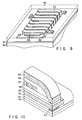
- a planar transformer which has a primary and secondary layered conductor coils wound around a magnetic thin film as shown in FIG. 9.
- a silicon substrate 50 having a thermal oxide film 51 formed thereon the lower conductor of a primary coil 52, the lower conductor of a secondary coil 53, a magnetic substance 54, the upper conductor of the primary coil 52 and the upper conductor of the secondary coil 53, each independently insulated, are layered.
- the lower conductor and upper conductor constituting each coil are formed in a predetermined pattern in the same manner as in Example 2 and connected to each other.
- the entire surface of the transformer is coated with a polyimide film 55. Pad holes are made at portions of the surface corresponding to both ends of the primary coil 52 and secondary coil 53.
- a thin-film magnetic head for a hard disk drive as shown in FIG. 10 can be manufactured.
- a silicon substrate 60 having a thermal oxide film 61 formed thereon SiO2 film 63 having an MR sensor 64 embedded therein, the lower core 65 made of CoZrNb amorphous soft magnetic thin film, SiO2 film 66 which forms a 0.1 ⁇ m recording gap at the end of the head, a layered conductor coil 67 formed in the same manner as in Example 2, a polyimide film 68 coated on the layered conductor coil 67, and an upper core 69 made of 2.0 ⁇ m-thick CoZrNb amorphous soft magnetic thin film are subsequently formed.
- the layered conductor wiring of the present invention can be used in a wiring of a semiconductor device.
Landscapes
- Engineering & Computer Science (AREA)
- Manufacturing & Machinery (AREA)
- Microelectronics & Electronic Packaging (AREA)
- Power Engineering (AREA)
- Chemical & Material Sciences (AREA)
- Inorganic Chemistry (AREA)
- Parts Printed On Printed Circuit Boards (AREA)
Abstract
Description
- The present invention relates to electronic devices having a layered conductor wiring using Cu as a main conductor, and to magnetic devices having a coil formed of such a layered conductor wiring.
- Recently, there has been a rapid progress in light-weight miniaturization of various electronic apparatuses. There is a strong demand for electronic devices constituting the electronic apparatuses to be smaller, thinner, and lighter than ever before. To satisfy the demands, a surface mounting device (SMD) is now widely employed. Furthermore, to integrate SMDs at a high density, studies have been conducted on a multi-chip module (MCM) comprising a multi-layer wiring substrate and a plurality of bare chips mounted on the substrate.
- In the multi-layer wiring substrate, it is required that the resistance of the wiring and the dielectric constant of the insulating material around the wiring should be low in order to reduce a signal transmission delay. To satisfy this requirement, Cu is used as a wiring conductor material and SiO₂, polyimide, or the like is used as a surrounding insulating material. If a structure is formed by contacting Cu directly with the insulating material, Cu will be diffused into SiO₂ or reacted with polyamic acid that is the precursor of the polyimide. Consequently, the dielectric constant of the insulating material decreases and further the wiring resistance increases, in some cases. Generally, in the prior art, a multi-layer wiring is formed so as not to contact Cu directly with the insulating material. For example, in the case where SiO₂ is used as the insulating material, Cu is coated with Ti or TiN to suppress Cu diffusion. On the other hand, when polyimide is used as the insulating material, Cu is coated with Ni or Ti to suppress the reaction between Cu and the precursor solution of the polyimide.
- Now, we will explain an example of a manufacturing process of a conventional multi-layer wiring substrate using Cu as the main conductor and polyimide as an insulating material.
- (a) First, on an insulating substrate made of, for example, alumina, a Ti film and a Cu film are sequentially formed by a vacuum deposition method or the like. The Ti film used herein is approximately 0.1 µm in thickness and is used as an underlying conductor exhibiting good adhesiveness to the substrate. The Cu film used herein is approximately 1 µm in thickness and is utilized as a conductor for a plating electrode which will be part of the main conductor. Thereafter, a thick resist film is coated over the entire surface of the above-obtained structure and is patterned by photolithography, thereby forming openings at a portion in which wiring is formed.
- (b) After Cu as the main conductor is allowed to grow by electroplating in the opening portion of the resist to a predetermined thickness, the resist is peeled off. As a coating for suppressing the reaction between the Cu main conductor and a polyimide precursor, a Ti film is formed by the vacuum deposition method or the like so as to cover an exposed Cu face.
- (c) A resist for removing a layered conductor (Ti/Cu/Ti) present in a space portion is patterned by photolithography. Thereafter, using the resist thus patterned as a mask, Ti and Cu are alternately etched by an enchant for removing Ti containing mainly of acetic acid, nitric acid and hydrofluoric acid, and by an etchant for removing Cu containing ferric chloride and water.
- (d) A polyimide film serving as an insulator is formed over the entire surface and contact holes are made therein.
- (e) The aforementioned steps (a) to (d) are repeated, thereby forming a multi-layer wiring. Finally, pad holes are made, and an Ni film having at least 1 µm in thickness and an Au film having at least 1 µm in thickness, both serving as a pad conductor, are sequentially formed by the vacuum deposition method or the like. After that, a resist (not shown) is patterned by photolithography. Using the resist pattern as a mask, Au and Ni present other than the pad portion are removed, thereby forming the pad conductor.
- However, the aforementioned prior art has the following problems:
- (1) It is difficult to control the alternate etching of Ti/Cu/Ti in Step (c) without failure. For example, when Cu is etched, a side etching of Cu is inevitable since Ti is scarcely etched. As a result, overhang of Ti occurs as shown in FIG. 1. If the overhang occurs in a lower portion of the conductor, air foams may be easily incorporated when a precursor of polyimide serving as an insulator is coated in a later step. Air foams, if incorporated in a multilayer wiring substrate, cause various problems.
- (2) Fabrication steps are complicated since patterning has to be performed after the pad portion is independently coated with a metal such as Ni or Au.
- Of the aforementioned problems, it is considered that problem (2) can be overcome by coating the main conductor made of Cu with Al or an Al alloy as described in, for example, Jpn. Pat. Appln. KOKAI Publication No. 60-128641. However, the Al or Al alloy coating Cu induces stress-migration, thermal-migration, or electro-migration which may further cause hillocks. The generated hillocks are likely to develop into a number of voids which possibly facilitate reaction of an exposed Cu portion with an insulator.
- Furthermore, the conductor material which is formed into a coil, is used in an planar inductor or transformer, and a thin-film magnetic head. In this case, also, Cu having a high conductivity is mostly used to reduce coil resistance. Hitherto, in such magnetic devices, a resist is widely used as an insulator between coil lines and of the upper portion of the coil lines (Amorphous Electron Device Research Institute, Research Report, April, 1994). This is because when polyimide or SiO₂ is used instead of a resist as an insulator, the same problems are caused as in the case of the multi-layer wiring substrate mentioned above, that is, difficulties associated with a process control and complexity of manufacturing steps. For example, in a thin-film magnetic head having a conductor consisting of Cu coated with Ni described in Jpn. Pat. Appln. KOKAI Publication No. 1-277311, the aforementioned problems are inevitably caused. When a resist is used as an insulator, due to poor thermal resistance of the resist, temperature of a process has to be reduced. In particular, when annealing is performed in the magnetic field to impart magnetic anisotropy to a magnetic substance, the uppermost temperature is restricted to a heat resistance temperature of the resist (approximately 200°C). For this reason, it is impossible to sufficiently reduce magnetic anisotropic dispersion, causing problematic deterioration in frequency characteristic.
- As described above, in electronic devices such as a multi-layer wiring substrate containing a layered conductor wiring using Cu as the main conductor, and in magnetic devices represented by an inductor, transformer and magnetic head, containing a planar coil formed of such layered conductor wiring, there are problems such as difficulties associated with a process control and complexity in manufacturing steps. Furthermore, since a process cost increases accompanying these problems, practical uses of the electronic devices and magnetic devices are delayed. Hence, they have not yet risen large-scale industrial demands.
- An object of the present invention is to improve controlling of a process and is to simplify manufacturing steps of a layered conductor wiring using Cu as the main conductor, thereby attaining a reduction of cost and practical uses of the electronic devices such as a multi-layer wiring substrate and of the magnetic devices such as an inductor, transformer, and magnetic head, all using the layered conductor wiring.
- The electronic device of the present invention comprises a conductor wiring enclosed with an underlying insulator and a surrounding insulator, the conductor wiring having an underlying conductor formed in a predetermined pattern on a surface of the underlying insulator and made of at least one selected from the group consisting of Ti, Ta, Mo, Cr, Nb, and W; a main conductor made of Cu formed on the underlying conductor in a predetermined pattern; a first coating conductor made of at least one selected from the group consisting of Ti, Ta, Mo, Nb, and Ni and a second coating conductor made of at least one selected from the group consisting of Au and Al that are formed in this order so as to coat the surface facing the surrounding insulator of the main conductor made of Cu.
- The magnetic devices of the present invention include, for example, those which have a coil formed by using the layered conductor wiring having the aforementioned structure.
- This invention can be more fully understood from the following detailed description when taken in conjunction with the accompanying drawings, in which:
- FIG. 1 is a cross-sectional view showing a conventional layered conductor wiring;
- FIG. 2 is a cross-sectional view showing an example of the layered conductor wiring according to the present invention;
- FIGS. 3A to 3C are cross-sectional views showing the layered conductor wiring according to the present invention;
- FIGS. 4A to 4E are cross-sectional views showing an example of the manufacturing process of the layered conductor wiring according to the present invention;
- FIGS. 5A to 5E are cross-sectional views showing another example of the manufacturing process of the layered conductor wiring according to the present invention;
- FIGS. 6A to 6E are cross-sectional views showing still another example of the manufacturing process of the layered conductor wiring according to the present invention;
- FIGS. 7A and 7B are a plan and cross-sectional views of the thin-film coil fabricated in Example 3 of the present invention;
- FIGS. 8A and 8B are a plan and cross-sectional views of a planar choke coil fabricated in Example 4 of the present invention;
- FIG. 9 is a perspective view of the planar transformer fabricated in another Example of the present invention; and
- FIG. 10 is a perspective view of the thin-film magnetic head fabricated in still another Example of the present invention.
- The layered conductor wiring according to one embodiment of the present invention is shown in FIG. 2. As shown in this figure, on an underlying insulator 1, an
underlying conductor 2 processed in a predetermined pattern and themain conductor 3 made of Cu are formed. If desired, for example to assist fabrication by electroplating, a conductor layer 3a for a plating electrode can be initially applied to the underlying insulator 1. Use of such a layer 3a is optional and not essential. If present, it can be regarded as a part of themain conductor 3, since the layer 3a and the main conductor must both be of copper. The surface facing a surrounding insulator of themain conductor 3 made of Cu is coated with afirst coating conductor 4 and asecond coating conductor 5. The surroundinginsulator 6 made of polyimide or SiO₂ is provided on the layered conductor wiring having such a structure. Furthermore, contact holes are formed in theinsulator 6, and abonding wire 10 made of Au or Al is connected to thesecond coating conductor 5. - As described above, as the underlying conductor, use is made of at least one type of metal selected from the group consisting of Ti, Ta, Mo, Cr, Nb, and W and their alloy. As the first coating conductor, use is made of at least one type of metal selected from the group consisting of Ti, Ta, Mo, Nb, and Ni and their alloy. As the second coating conductor, use is made of at least one type of metal selected from the group consisting of Au and Al and their alloy.
- The thickness of the
underlying conductor 2 is preferably 0.05 µm or more, the thickness of the first andsecond coating conductors underlying conductor 2 is extremely thin, a failure in adhesion will occur due to diffusion of Cu. In contrast, if the thickness of thesecond coating conductors underlying conductor 2, the first andsecond coating conductors main conductor 3 made of Cu. The uppermost thickness, although varies depending on usage, is generally 10 µm or less. - In the layered wiring according to the present invention, by selecting an appropriate metal species from the metal group mentioned above as the
underlying conductor 2, the first andsecond coating conductors - It will be appreciated that the side edges of 2, 3, (3a if present), 4 and 5 can be co-planar and mutually adjacent forming on practice a single, planar edge on each side of the device at the respective ends of those layers, or they can be parallel such that there are no voids or gaps in the region of those edges, and a single planar edge is similarly formed on each side of the device immediately above the underlying insulator.
- Cu as a main conductor is protected from SiO₂ or polyimide used as an insulator between adjacent conductors or an interlayer conductor applied in a multi-layer conductor, thereby suppressing Cu diffusion into SiO₂ and a reaction of Cu with polyimide.
- Furthermore, since the first coating conductor interposed between the main conductor made of Cu and the second coating conductor made of Al, Au or an Al-Au alloy is a metal having a high melting point, the metal itself rarely causes migration, with the result that hillocks developing into voids are not generated. Owing to this, Cu will not be exposed and the conductor wiring using Cu as the main conductor will be improved in reliability.
- Since the first coating conductor positioned in the lower portion of the second coating conductor (Al or/and Au) is a hard material, even if the second coating conductor, which is exposed by forming contact holes in the
insulator 6 on the wiring, is used as a pad portion, and a bonding wire made of Al or Au is directly wedge-bonded or ball-bonded thereto, sufficient mechanical strength will be maintained. Accordingly, a step of depositing a metal onto a pad portion and patterning it, is no longer necessary, thereby shortening manufacturing steps. - In the layered conductor wiring according to the present invention, the main conductor made of Cu, the underlying conductor (hereinafter, referred to as "Metal A"), the first coating conductor (hereinafter, referred to as "Metal B") and the second coating conductor (hereinafter, referred to as "Metal C") may be formed by the vacuum deposition, sputtering method, or the like. Alternatively, thick Cu film may be formed as the main conductor by electroplating using a previously-formed Cu film as an electrode. The manufacturing process will be more specifically explained with reference to FIGS. 4A to 4E, FIGS. 5A to 5E, and FIGS. 6A to 6E.
- FIGS. 4A to 4E show an example of the manufacturing steps in the case where Cu as the main conductor is formed into a thin film of less than 10 µm in thickness by the vacuum deposition or the sputtering method. First, on an insulating substrate 1, an
underlying conductor 2 made of Metal A, which strengthens the adhesiveness to the substrate, and amain conductor 3 made of Cu are formed. Upon the structure thus obtained, aphotoresist 21 is formed in a predetermined pattern (FIG. 4A). Subsequently, using thephotoresist 21 as a mask, Cu and Metal A are etched together with an etchant (FIG. 4B). Thereafter, over the entire surface of the above-obtained structure, afirst coating conductor 4 made of Metal B and asecond coating conductor 5 made of Metal C are sequentially formed (FIG. 4C). After that, aphotoresist 22 is formed in a predetermined pattern so as to cover the main conductor line by photolithography (FIG. 4D). Then, using thephotoresist 22 as a mask, Metals C and B present in the area other than the main conductor line are etched together (FIG. 4E). - In this method, Metal A and the etchant 1 used in the step of FIG. 4B should be chosen in such a way that the relationship of etching rates in the etchant 1 satisfy the following condition:

- Metals C, B and the
etchant 2 used in the step of FIG. 4E should be chosen in such way that the relationship of etching rates in theetchant 2 satisfy the following condition:
- In this way, by choosing an appropriate metal species and an etchant, the lower portion of the wiring may be formed as shown in FIG. 3A and overhang will not be generated.
- FIGS. 5A to 5E show an example of the manufacturing steps in the case where the main conductor made of Cu is formed into a thick film of 10 µm or more in thickness by electroplating. First, on an insulating substrate 1, an
underlying conductor 2 made of Metal A, which strengthens the adhesiveness to the substrate, and a conductor 3a for a plating electrode made of Cu which will be part of the main conductor, are formed. On the structure thus obtained, aphotoresist 23 is formed in a predetermined pattern (FIG. 5A). Subsequently, using an appropriate plating solution, the main conductor made of Cu is allowed to grow on the conductor 3a for a plating electrode which exposed from aphotoresist 23 and then thephotoresist 23 is removed (FIG. 5B). Subsequently, over the entire surface of the above-obtained structure, afirst coating conductor 4 made of Metal B and asecond coating conductor 5 made of Metal C are sequentially formed (FIG. 5C). After that, aphotoresist 24 is formed by photolithography in a predetermined pattern so as to cover the main conductor line (FIG. 5D). Further, using thephotoresist 24 as a mask, Metals C and B, Cu and Metal A present in the area other than the main conductor line are etched together with an etchant(FIG. 5E). - In this method, Metals C, B, A and the etchant used in the step of FIG. 5E should be chosen in such a way that the relationship of etching rates in the etchant satisfy the following condition:

- In this way, by choosing an appropriate metal species and an etchant, the lower portion of the wiring may be formed as shown in FIG. 3B and overhang will not be generated.
- FIGS. 6A to 6E show an example of the manufacturing steps using electroplating. First, on an insulating substrate 1, an
underlying conductor 2 made of Metal A and a conductor 3a for a plating electrode made of Cu which will be part of the main conductor are formed in the same manners as in FIG. 5A. Further, on the above-obtained structure, a photoresist is formed in a predetermined pattern and themain conductor 3 made of Cu is allowed to grow by electroplating and then the photoresist is removed in the same manners as in FIG. 5B. - Subsequently, a
photoresist 25 is formed in a predetermined pattern so as to cover the main conductor line (FIG. 6A). Thereafter, using thephotoresist 25 as a mask, Cu and Metal A are etched together with an etchant (FIG. 6B). Then, over the entire surface, afirst coating conductor 4 made of Metal B and asecond coating conductor 5 made of Metal C are sequentially formed (FIG. 6C). After that, aphotoresist 26 is formed by photolithography in a predetermined pattern so as to cover the main conductor line (FIG. 6D). Then, using thephotoresist 26 as a mask, Metals C and B present in the area other than the main conductor line are etched together with an etchant (FIG. 6E). - Also in this method, Metal A and the etchant 1 used in the step of FIG. 6B should be chosen in such a way that the relationship of etching rates in the etchant 1 satisfy the condition given by aforementioned formula (1). Metals C, B and the
etchant 2 used in the step of FIG. 6E should be chosen in such a way that the relationship of etching rates in theetchant 2 satisfy the condition given by the aforementioned formula (2). - In this way, by choosing an appropriate metal species and an etchant, the lower portion of the wiring may be formed as shown in FIG. 3C and overhang will not be generated.
- A combination of a metal and an etchant satisfying the conditions given by formulas (1) to (3) may be uncountable. By way of reference of choosing a metal and an etchant satisfying predetermined conditions, the relative etching abilities of various types of metal elements to various etchants are listed in Table 1. With respect to a given etchant shown in Table 1, a metal susceptible to etching at room temperature is indicated as ⓞ; a metal susceptible to etching at 100°C is indicated as ○; and a metal insusceptible to etching is indicated as "x". Under predetermined etching conditions, the etching rate gets slower in sequential order of ⓞ to "x". Hence, with reference to this Table, the metal and etchant to be chosen can be determined.


- Hereinbelow, Examples of the present invention will be explained with reference to Figures.
- In accordance with manufacturing steps shown in FIGS. 4A to 4E, a layered conductor wiring is manufactured.
- First, on the surface of an alumina substrate, a 0.1 µm-thick Mo film as an underlying conductor and a 5 µm-thick Cu film as the main conductor are sequentially formed by the vacuum deposition method. Thereafter, a photoresist pattern corresponding to a circuit pattern is formed by photolithography. Subsequently, using this photoresist pattern as a mask and a mixed solution consisting of phosphoric acid (77 vol%), nitric acid (3 vol%), acetic acid (15 vol%) and water (5 vol%) as an etchant, the 5 µm-thick Cu film and the 0.1 µm-thick Mo film are etched together. The etching rate of Cu herein is approximately 0.4 µm/min, and that of Mo is approximately 0.1 µm/min.
- Second, over the entire surface, a 1 µm-thick Mo film as a first coating conductor and a 1 µm-thick Al film as a second coating conductor are sequentially formed by the vacuum deposition method. Subsequently, a photoresist pattern is formed so as to enclose the Cu/Mo wiring line. Using this photoresist pattern as a mask, and a mixed solution of phosphoric acid (95.4 vol%), nitric acid (0.6 vol%), acetic acid (3.0 vol%) and water (1.0 vol%) as an etchant, the 1 µm-thick Mo film and the 1 µm-thick Al film are etched together. The etching rate of Mo herein is approximately 0.05 µm/min, and that of Al is approximately 0.08 µm/min. Through these steps, a layered conductor wiring is successfully formed, with no overhang in the lower portion as shown in FIG. 3A.
- Thereafter, polyamic acid as a polyimide precursor is spin-coated onto the entire surface so as not to incorporate air foams therein under reduced pressure, in an atmosphere of its solvent, followed by curing at 350°C for 120 minutes. On the polyimide insulator thus cured, a photoresist pattern for use in making contact holes is formed. Using this photoresist as a mask, chemical dry etching (CDE) using mixed gas of oxygen and carbon tetrafluoride is applied to the polyimide to form contact holes. Furthermore, on the thus obtained structure, layered conductor wirings constituting the second layers or above are sequentially formed, thereby preparing a multi-layer wiring substrate.
- In accordance with manufacturing steps shown in FIGS. 6A to 6E, a layered conductor wiring is manufactured as follows:
- First, on a silicon substrate having a 0.2 µm-thick thermal oxide film on the surface thereof, a 0.1 µm-thick Mo film as an underlying conductor and a 1 µm-thick Cu film as a plating electrode conductor are subsequently formed by a DC magnetron sputtering method. After a photoresist pattern corresponding to a reversal pattern of a circuit pattern is formed by photolithography, Cu serving as the main conductor is electroplating onto the Cu film to 40 µm in thickness at a current density of 15 mA/cm, using a solution containing mainly sulfuric acid, copper sulfate, and hydrochloric acid. Thereafter, the resist is removed with acetone and the resultant structure is washed in pure water. Since the plated conductor has a reverse tapered form having an angle of 80°, if the resist pattern, whose width is slightly narrower than that of the plated conductor, is formed on the plated Cu conductor line as a mask and etching is performed with an etchant, i.e., a mixed solution of phosphoric acid (77 vol%), nitric acid (3 vol%), acetic acid (15 vol%) and water (5 vol%), excessive Cu can be removed. As a result, the width of the plated conductor line is slightly reduced but the reverse tapered portions almost disappear. At this time, simultaneously the Cu film is slightly etched away from the area (space portions) other than the lines. The Cu etching rate herein is 0.4 µm/min.
- Thereafter, a photoresist pattern is formed so as to enclose the plated Cu conductor line. Using the photoresist pattern as a mask and a mixed solution of phosphoric acid (77 vol%), nitric acid (3 vol%), acetic acid (15 vol%) and water (5 vol%) as an etchant, the Cu film and Mo film of the space portions are etched away together. The Cu etching rate herein is 0.4 µm/min, and the Mo etching rate is 0.1 µm/min.
- Subsequently, over the entire surface, 1 µm-thick Mo film as a first coating conductor and 1 µm-thick Al film as a second coating conductor are subsequently formed by the DC magnetron sputtering method. At this time, the Mo and Al films are formed under suitable conditions that a good step coverage is established, for example, under a raised Ar gas pressure, thereby coating a side wall of the 40 µm-thick Cu conductor with the Mo and Al films of 0.5 µm or more in thickness. After that, a photoresist pattern is formed so as to enclose the conductor line. Using the photoresist pattern as a mask, and a mixed solution of phosphoric acid (95.4 vol%), nitric acid (0.6 vol%), acetic acid (3.0 vol%) and water (1.0 vol%) as an etchant, the 1 µm-thick Mo film and 1 µm-thick Al film are etched away together. The Mo etching rate herein is approximately 0.05 µm/min and the Al etching rate is approximately 0.08 µm/min.
- Through these steps, a thick-film layered conductor wiring can be formed with no overhang in the lower portion as shown in FIG. 3C.
- Subsequently, polyimide is formed in the same manner as in Example 1 and contact holes are made by chemical dry etching. Furthermore, on the above-obtained structure, layered conductor wirings constituting circuit patterns of the second layer or above are sequentially formed, thereby forming a multilayer thick-film wiring substrate.
- A planar thin-film coil shown in FIGS. 7A and 7B is manufactured in accordance with the steps of the Example 1. FIG. 7A is a plan view and FIG. 7B is a cross-sectional view. In FIGS. 7A and 7B, on an
alumina substrate 31, aplanar coil 32 consisting of a mono-layered conductor wiring having a structure shown in FIG. 3A. The planar thin-film coil has a square spiral pattern with a number of turns of 5. The line and space of the layered conductor are 20 µm in width, an outer size of the square spiral coil is 500 µm. Subsequently, anSiO₂ film 33 serving as an insulating film between conductor lines and a protection film is coated over the entire surface by the plasma CVD method. Thereafter, using a resist as a mask,pad portions 34 are made by the RIE method using carbon tetrafluoride as reaction gas. Thereby an Al surface is exposed. - The coil functions normally as a direct current choke for a power amplifier used in an 800 MHz analog mobile phone.
- A planar choke coil for an MHz switching power source, shown in FIGS. 8A and 8B, is manufactured in accordance with the steps of Example 2. FIG. 8A is a plan view and FIG. 8B is a cross-sectional view. In FIGS. 8A and 8B, on a
silicon substrate 40 having athermal oxide film 41 on the surface thereof, a lower magneticthin film 42, anSiO₂ film 43, acoil 44, apolyimide film 45, an upper magneticthin film 46, and apolyimide film 47 are subsequently formed. Thecoil 44 is sandwiched between the upper magneticthin film 46 and the lower magneticthin film 42. In this choke coil, uniaxial magnetic anisotropy is imparted to the magnetic thin films, of which easy axis of magnetization is indicated by an arrow in FIG. 8A, so that the magnetic thin films are excited in the direction of the hard axis of magnetization in almost all area of the device. - Hereinafter, a manufacturing process of the choke coil will be explained in detail. On a
silicon substrate 40 having athermal oxide film 41 formed thereon, 0.1 µm-thick Al, AlNx (x = 0 - 0.5) and AlNx (x = 0.5 - 1) films (not shown) are sequentially formed to improve adhesiveness of the lower magnetic thin film. On the AlNx (x = 0.5 - 1) film, a 6.0 µm-thick lower magneticthin film 42 is formed. The magneticthin film 42 is of FeCoBC-based and hetero amorphous magnetic film in which an amorphous magnetic phase rich in FeCo and an amorphous insulating phase rich in boron and carbon are homogeneously dispersed. The saturation magnetic flux density of thefilm 42 is 1.6 T, the relative magnetic permeability in the direction of the hard axis of magnetization is 1100, and resistivity is 300 µΩ·cm. Using a resist pattern as a mask and a mixed solution of phosphoric acid (77 vol%), nitric acid (3 vol.%), acetic acid (15 vol%) and water (5 vol%) as an etchant, the magnetic thin film is etched. On this structure, 5.0 µm-thick SiO₂ film 43 is formed by sputtering. On thefilm 43, acoil 44 consisting of a layered conductor having a cross-sectional structure shown in FIG. 3C is formed in the same manner as in Example 2. Thecoil 44 has a pattern in which two rectangular spiral coils, one is a right handed spiral, the other is a left handed spiral, are juxtaposed to each other. The number of turns of the coil is 6. The thickness of the Cu conductor is 50 µm. Subsequently, apolyimide film 45 is formed between lines of thecoil 44 and on the lines in the same manner as in Example 1. After the surface of thepolyimide film 45 is sufficiently made flat, a 6 µm-thick upper magneticthin film 46 is formed of the same material as that employed in the lower magneticthin film 42 and etched in the same manner as in the case of the lower magneticthin film 42. Further, over thefilm 46, apolyimide film 47 is formed as a protecting film. Subsequently, a resist pattern is formed in order to make holes in pad portions. Using the resist pattern as a mask, thepolyimide film 47 is etched by chemical dry etching using mixture gas of oxygen and carbon tetrafluoride and thereby the Al surface of the pad portion is exposed. Finally, a direct current magnetic field of 4 kA/m is applied to the magnetic thin films in the direction of an arrow shown in FIG. 8A in vacuum and then the films are subjected to heat treatment at 320°C to impart uniaxial magnetic anisotropy. Alternatively, the uniaxial magnetic anisotropy can be imparted by forming a soft magnetic thin film in a direct current magnetic field. - The planar choke coil thus obtained has an inductance of 0.5 µH and a direct current coil resistance of 0.2 Ω. Further, a direct current at which the inductance reduces by 50% is 1.5A.
- A control IC, MOSFET for switching, and a Schottoky diode for rectification, all are bare chips, and the choke coil are bonded to each other with an Au wire of 50 µm in diameter, thereby forming a boost chopper type DC to DC converter functioning at 5 MHz. This converter is capable of raising a 3.6 V input voltage to 5.0 V and its power conversion efficiency is 82% at the time when 3.0 W of power is output.
- Other than the aforementioned Examples, various electronic devices and magnetic devices can be manufactured by applying the present invention as described follows:
- For example, in accordance with the same manufacturing process of the layered conductor wiring as in Example 2, a planar transformer can be formed, which has a primary and secondary layered conductor coils wound around a magnetic thin film as shown in FIG. 9. In FIG.9, on a silicon substrate 50 having a
thermal oxide film 51 formed thereon, the lower conductor of aprimary coil 52, the lower conductor of asecondary coil 53, amagnetic substance 54, the upper conductor of theprimary coil 52 and the upper conductor of thesecondary coil 53, each independently insulated, are layered. The lower conductor and upper conductor constituting each coil are formed in a predetermined pattern in the same manner as in Example 2 and connected to each other. The entire surface of the transformer is coated with apolyimide film 55. Pad holes are made at portions of the surface corresponding to both ends of theprimary coil 52 andsecondary coil 53. - Furthermore, a thin-film magnetic head for a hard disk drive as shown in FIG. 10 can be manufactured. In FIG. 10, on a silicon substrate 60 having a
thermal oxide film 61 formed thereon,SiO₂ film 63 having anMR sensor 64 embedded therein, the lower core 65 made of CoZrNb amorphous soft magnetic thin film,SiO₂ film 66 which forms a 0.1 µm recording gap at the end of the head, alayered conductor coil 67 formed in the same manner as in Example 2, a polyimide film 68 coated on thelayered conductor coil 67, and anupper core 69 made of 2.0 µm-thick CoZrNb amorphous soft magnetic thin film are subsequently formed. - Furthermore, other than Examples mentioned above, the layered conductor wiring of the present invention can be used in a wiring of a semiconductor device.
Claims (11)
- An electronic or magnetic device having a conductor wiring enclosed by an underlying insulator (1) and a surrounding insulator (6),
characterized in that said conductor wiring comprises
an underlying conductor (2) formed in a predetermined pattern on a surface of the underlying insulator (1) and made of at least one of: Ti, Ta, Mo, Cr, Nb and W and an alloy of one or more thereof;
a main conductor (3) made of Cu formed in a predetermined pattern on said underlying conductor (2);
a first coating conductor (4) made of at least one of: Ti, Ta, Mo, Nb and Ni and an alloy of one or more thereof, and
a second coating (5) conductor made of at least one of: Au, A1 and an alloy thereof;
said coatings formed in this order to provide a surface coating on the surface of said main conductor which faces said surrounding insulator (6). - A magnetic device according to claim 1 including at least one coil formed from conductor wiring as defined in claim 1.
- A device according to claim 1 or 2, characterized in that said underlying conductor (2) has a thickness of 0.05 to 10 µm.
- A device according to any preceding claim, characterized in that said first and second coating conductors (4, 5) have a thickness of 0.5 to 10 µm.
- A device according to claim 4, characterized in that said first and second coating conductors (4, 5) have a thickness of 1 to 10 µm.
- A magnetic device according to any one of claims 2 to 6 wherein the or each coil is of planar form.
- A method of making an electronic or magnetic device having a conductor wiring enclosed with an underlying insulator (1) and a surrounding insulator (6),
characterized in that said conductor wiring comprises:
an underlying conductor (2) formed in a predetermined pattern on a surface of an underlying insulator (1) and made of at least one of:
Ti, Ta, Mo, Cr, Nb and W and an alloy of one or more thereof,
a main conductor (3) made of Cu formed in a predetermined pattern on said underlying conductor (2); and
first and second coating conductors (4, 5) which includes forming an exposed surface of said main conductor (3) made of Cu by alternately forming at least one first coating conductor layer of at least one of Ti, Ta, Mo, Nb and Ni and an alloy of one or more thereof and at least one second coating conductor layer of at least one of: Au, Al and an alloy, thereof followed by removing a portion by etching. - A method of making a device according to any preceding claim, characterised in that when said main conductor (3) made of Cu and underlying conductor (2) are simultaneously etched with a first etchant, if etching rates of said main conductor (3) and underlying conductor (2) are defined as R1.Cu and R1.A, respectively, said etching rates should satisfy the following relationship:

when said first and second coating conductors (4, 5) are simultaneously etched with a second etchant, if etching rates of said first and second coating conductors (4, 5) are defined as R2.B and R2.C, respectively, said etching rates should satisfy the following relationship:
- A method of making a device according to any one of claims 1 to 7, characterized in that when said main conductor (3) made of Cu, said underlying conductor (2), and said first and second coating conductors (4, 5) are simultaneously etched with an etchant, if etching rates of said main conductor (3), underlying conductor (2) and first and second coating conductors (4, 5) are defined as RCu, RA, RB and RC, respectively, said etching rates should satisfy the following relationship:

- An electric device according to any one of claims 1 to 6, characterized in that a plurality of said conductor wirings are layered to form a multi-layered wiring.
- A device according to any one of claims 1 to 6 or 10 which is one of the following:
a planar thin film coil, a planar choke coil, a planar transformer, a thin film magnetic head, a semiconductor or an inductor.
Applications Claiming Priority (2)
| Application Number | Priority Date | Filing Date | Title |
|---|---|---|---|
| JP22144494 | 1994-09-16 | ||
| JP221444/94 | 1994-09-16 |
Publications (2)
| Publication Number | Publication Date |
|---|---|
| EP0702379A1 true EP0702379A1 (en) | 1996-03-20 |
| EP0702379B1 EP0702379B1 (en) | 1997-12-17 |
Family
ID=16766837
Family Applications (1)
| Application Number | Title | Priority Date | Filing Date |
|---|---|---|---|
| EP95306536A Expired - Lifetime EP0702379B1 (en) | 1994-09-16 | 1995-09-15 | Electronic and/or magnetic devices |
Country Status (3)
| Country | Link |
|---|---|
| US (1) | US5738931A (en) |
| EP (1) | EP0702379B1 (en) |
| DE (1) | DE69501243T2 (en) |
Cited By (4)
| Publication number | Priority date | Publication date | Assignee | Title |
|---|---|---|---|---|
| EP1009029A1 (en) * | 1998-12-10 | 2000-06-14 | Sony Corporation | Semiconductor device and method of producing the same |
| FR2841381A1 (en) * | 2002-06-24 | 2003-12-26 | Nec Electronics Corp | INTEGRATED SEMICONDUCTOR CIRCUIT AND A METHOD FOR MANUFACTURING THE CIRCUIT |
| WO2015125460A1 (en) * | 2014-02-18 | 2015-08-27 | Skyworks Panasonic Filter Solutions Japan Co., Ltd. | Acoustic wave elements and ladder filters using same |
| US20170196081A1 (en) * | 2016-01-04 | 2017-07-06 | At&S (China) Co. Ltd. | Component Carrier With Different Surface Finishes |
Families Citing this family (26)
| Publication number | Priority date | Publication date | Assignee | Title |
|---|---|---|---|---|
| TW444252B (en) * | 1999-03-19 | 2001-07-01 | Toshiba Corp | Semiconductor apparatus and its fabricating method |
| JP2000322709A (en) * | 1999-05-13 | 2000-11-24 | Alps Electric Co Ltd | Thin film element and its production |
| JP3363832B2 (en) * | 1999-05-13 | 2003-01-08 | アルプス電気株式会社 | Thin film structure and method of manufacturing the same |
| US6369983B1 (en) * | 1999-08-13 | 2002-04-09 | Read-Rite Corporation | Write head having a dry-etchable antireflective intermediate layer |
| JP2001244123A (en) | 2000-02-28 | 2001-09-07 | Kawatetsu Mining Co Ltd | Surface mount type planar magnetic element and method of manufacturing the same |
| JP3320397B2 (en) * | 2000-03-09 | 2002-09-03 | クラリアント ジャパン 株式会社 | Method of forming reverse tapered resist pattern |
| US6653573B2 (en) | 2000-04-04 | 2003-11-25 | Nec Tokin Corporation | Wiring board comprising granular magnetic film |
| JP2001307313A (en) * | 2000-04-20 | 2001-11-02 | Fujitsu Ltd | Manufacturing method of thin film head |
| TWI312166B (en) * | 2001-09-28 | 2009-07-11 | Toppan Printing Co Ltd | Multi-layer circuit board, integrated circuit package, and manufacturing method for multi-layer circuit board |
| JP3775499B2 (en) * | 2002-01-08 | 2006-05-17 | 株式会社リコー | Semiconductor device, manufacturing method thereof, and DC-DC converter |
| JP2005261987A (en) * | 2002-09-06 | 2005-09-29 | Joiaasu Kk | Activation apparatus |
| US7358195B2 (en) * | 2003-04-01 | 2008-04-15 | Lg.Philips Lcd Co., Ltd. | Method for fabricating liquid crystal display device |
| JP4268434B2 (en) * | 2003-04-09 | 2009-05-27 | 大日本印刷株式会社 | Wiring board manufacturing method |
| JP2005191408A (en) * | 2003-12-26 | 2005-07-14 | Matsushita Electric Ind Co Ltd | Coil conductor, manufacturing method thereof, and electronic component using the same |
| JP2006154569A (en) * | 2004-11-30 | 2006-06-15 | Tokyo Ohka Kogyo Co Ltd | Method for producing resist pattern and conductor pattern |
| JO3058B1 (en) | 2005-04-29 | 2017-03-15 | Applied Molecular Evolution Inc | Anti-IL-6 Antibodies,Compositions,Methods and uses |
| TWI277373B (en) * | 2005-09-16 | 2007-03-21 | Foxconn Advanced Tech Inc | Method of continuous producing flexible printed circuit board |
| CN101796723B (en) * | 2007-10-30 | 2013-07-17 | 太阳诱电株式会社 | Elastic wave element, duplexer, communication module, and communication apparatus |
| US8188235B2 (en) | 2008-06-18 | 2012-05-29 | Pfizer Inc. | Antibodies to IL-6 and their uses |
| US8445375B2 (en) * | 2009-09-29 | 2013-05-21 | Semiconductor Components Industries, Llc | Method for manufacturing a semiconductor component |
| TWM397591U (en) * | 2010-04-22 | 2011-02-01 | Mao Bang Electronic Co Ltd | Bumping structure |
| US9425146B2 (en) * | 2010-09-28 | 2016-08-23 | Infineon Technologies Ag | Semiconductor structure and method for making same |
| US20130241058A1 (en) * | 2012-03-16 | 2013-09-19 | Taiwan Semiconductor Manufacturing Company, Ltd. | Wire Bonding Structures for Integrated Circuits |
| DE102016216308B4 (en) | 2016-08-30 | 2022-06-15 | Schweizer Electronic Ag | Circuit board and method for its manufacture |
| JPWO2018092172A1 (en) | 2016-11-15 | 2018-11-15 | 信越化学工業株式会社 | High efficiency solar cell and method of manufacturing high efficiency solar cell |
| WO2020045436A1 (en) * | 2018-08-28 | 2020-03-05 | 京セラ株式会社 | Wiring board and electronic device |
Citations (3)
| Publication number | Priority date | Publication date | Assignee | Title |
|---|---|---|---|---|
| JPS60128641A (en) | 1983-12-16 | 1985-07-09 | Hitachi Ltd | Multilayer interconnection |
| US4760481A (en) * | 1986-07-11 | 1988-07-26 | Hitachi, Ltd. | Thin film magnetic head having an improved coil |
| JPH01277311A (en) | 1988-04-28 | 1989-11-07 | Hitachi Ltd | thin film magnetic head |
Family Cites Families (4)
| Publication number | Priority date | Publication date | Assignee | Title |
|---|---|---|---|---|
| DE2040180B2 (en) * | 1970-01-22 | 1977-08-25 | Intel Corp, Mountain View, Calif. (V.St.A.) | METHOD FOR PREVENTING MECHANICAL BREAKAGE OF A THIN ELECTRICALLY CONDUCTIVE LAYER COVERING THE SURFACE OF A SEMICONDUCTOR BODY |
| US3862017A (en) * | 1970-02-04 | 1975-01-21 | Hideo Tsunemitsu | Method for producing a thin film passive circuit element |
| GB1527894A (en) * | 1975-10-15 | 1978-10-11 | Mullard Ltd | Methods of manufacturing electronic devices |
| JPS59126665A (en) * | 1983-01-10 | 1984-07-21 | Hitachi Ltd | Thick film hybrid integrated circuit |
-
1995
- 1995-09-13 US US08/527,868 patent/US5738931A/en not_active Expired - Fee Related
- 1995-09-15 EP EP95306536A patent/EP0702379B1/en not_active Expired - Lifetime
- 1995-09-15 DE DE69501243T patent/DE69501243T2/en not_active Expired - Fee Related
Patent Citations (3)
| Publication number | Priority date | Publication date | Assignee | Title |
|---|---|---|---|---|
| JPS60128641A (en) | 1983-12-16 | 1985-07-09 | Hitachi Ltd | Multilayer interconnection |
| US4760481A (en) * | 1986-07-11 | 1988-07-26 | Hitachi, Ltd. | Thin film magnetic head having an improved coil |
| JPH01277311A (en) | 1988-04-28 | 1989-11-07 | Hitachi Ltd | thin film magnetic head |
Non-Patent Citations (3)
| Title |
|---|
| AMORPHOUS ELECTRON DEVICE RESEARCH INSTITUTE: "Research Report", April 1994 |
| PATENT ABSTRACTS OF JAPAN vol. 009, no. 288 (E - 358) 15 November 1985 (1985-11-15) * |
| PATENT ABSTRACTS OF JAPAN vol. 014, no. 048 (P - 0997) 29 January 1990 (1990-01-29) * |
Cited By (8)
| Publication number | Priority date | Publication date | Assignee | Title |
|---|---|---|---|---|
| EP1009029A1 (en) * | 1998-12-10 | 2000-06-14 | Sony Corporation | Semiconductor device and method of producing the same |
| FR2841381A1 (en) * | 2002-06-24 | 2003-12-26 | Nec Electronics Corp | INTEGRATED SEMICONDUCTOR CIRCUIT AND A METHOD FOR MANUFACTURING THE CIRCUIT |
| US7053165B2 (en) | 2002-06-24 | 2006-05-30 | Nec Electronics Corporation | Semiconductor integrated circuit including an inductor and method of manufacturing the same |
| WO2015125460A1 (en) * | 2014-02-18 | 2015-08-27 | Skyworks Panasonic Filter Solutions Japan Co., Ltd. | Acoustic wave elements and ladder filters using same |
| US9614495B2 (en) | 2014-02-18 | 2017-04-04 | Skyworks Filter Solutions Japan Co., Ltd. | Elastic wave element with a reinforcement electrode and ladder filter using same |
| US10389326B2 (en) | 2014-02-18 | 2019-08-20 | Skyworks Filter Solutions Japan Co., Ltd. | Methods of reducing electric loss in elastic wave elements |
| US20170196081A1 (en) * | 2016-01-04 | 2017-07-06 | At&S (China) Co. Ltd. | Component Carrier With Different Surface Finishes |
| US10806027B2 (en) * | 2016-01-04 | 2020-10-13 | At&S (China) Co. Ltd. | Component carrier with different surface finishes |
Also Published As
| Publication number | Publication date |
|---|---|
| DE69501243D1 (en) | 1998-01-29 |
| DE69501243T2 (en) | 1998-05-20 |
| EP0702379B1 (en) | 1997-12-17 |
| US5738931A (en) | 1998-04-14 |
Similar Documents
| Publication | Publication Date | Title |
|---|---|---|
| EP0702379B1 (en) | Electronic and/or magnetic devices | |
| US7021518B2 (en) | Micromagnetic device for power processing applications and method of manufacture therefor | |
| US6903645B2 (en) | Surface mounting type planar magnetic device and production method thereof | |
| EP1063661B1 (en) | An integrated circuit having a micromagnetic device and method of manufacture therefor | |
| US6696744B2 (en) | Integrated circuit having a micromagnetic device and method of manufacture therefor | |
| US6992871B2 (en) | Microtransformer for system-on-chip power supply | |
| US6853522B2 (en) | Microtransformer for system-on-chip power supply | |
| JP3580054B2 (en) | Thin film magnetic element and method of manufacturing the same | |
| US20080143469A1 (en) | Magnetic device | |
| US6191495B1 (en) | Micromagnetic device having an anisotropic ferromagnetic core and method of manufacture therefor | |
| US6420954B1 (en) | Coupled multilayer soft magnetic films for high frequency microtransformer for system-on-chip power supply | |
| JP2000114047A (en) | Thin-film transformer and manufacture thereof | |
| JP3544758B2 (en) | Electronic and magnetic components | |
| JP3765366B2 (en) | Planar magnetic element integrated semiconductor device | |
| JPH0955316A (en) | Planar magnetic element and manufacturing method thereof | |
| JPH05109557A (en) | High frequency thin film transformer and high frequency thin film inductor | |
| JP3195106B2 (en) | Manufacturing method of planar magnetic element | |
| JPS63283004A (en) | Planar inductor and its manufacturing method | |
| JP2001196252A (en) | Manufacturing method of electronic device | |
| US20230386720A1 (en) | Inductor | |
| JP3146672B2 (en) | A thin-film laminated magnetic induction element and an electronic device using the same. | |
| JP2000091142A (en) | Magnetic component with lead and noise reduction circuit using the same | |
| JPH11329840A (en) | Planar magnetic element and method of manufacturing the same | |
| JPH05109556A (en) | High frequency thin film transformer and high frequency thin film inductor | |
| JP2000164426A (en) | Thin film inductor and manufacture thereof |
Legal Events
| Date | Code | Title | Description |
|---|---|---|---|
| PUAI | Public reference made under article 153(3) epc to a published international application that has entered the european phase |
Free format text: ORIGINAL CODE: 0009012 |
|
| 17P | Request for examination filed |
Effective date: 19951011 |
|
| AK | Designated contracting states |
Kind code of ref document: A1 Designated state(s): DE FR GB |
|
| 17Q | First examination report despatched |
Effective date: 19960429 |
|
| GRAG | Despatch of communication of intention to grant |
Free format text: ORIGINAL CODE: EPIDOS AGRA |
|
| GRAH | Despatch of communication of intention to grant a patent |
Free format text: ORIGINAL CODE: EPIDOS IGRA |
|
| GRAH | Despatch of communication of intention to grant a patent |
Free format text: ORIGINAL CODE: EPIDOS IGRA |
|
| GRAA | (expected) grant |
Free format text: ORIGINAL CODE: 0009210 |
|
| AK | Designated contracting states |
Kind code of ref document: B1 Designated state(s): DE FR GB |
|
| REF | Corresponds to: |
Ref document number: 69501243 Country of ref document: DE Date of ref document: 19980129 |
|
| ET | Fr: translation filed | ||
| PLBE | No opposition filed within time limit |
Free format text: ORIGINAL CODE: 0009261 |
|
| STAA | Information on the status of an ep patent application or granted ep patent |
Free format text: STATUS: NO OPPOSITION FILED WITHIN TIME LIMIT |
|
| 26N | No opposition filed | ||
| REG | Reference to a national code |
Ref country code: GB Ref legal event code: IF02 |
|
| PGFP | Annual fee paid to national office [announced via postgrant information from national office to epo] |
Ref country code: FR Payment date: 20080915 Year of fee payment: 14 |
|
| PGFP | Annual fee paid to national office [announced via postgrant information from national office to epo] |
Ref country code: GB Payment date: 20080917 Year of fee payment: 14 |
|
| PGFP | Annual fee paid to national office [announced via postgrant information from national office to epo] |
Ref country code: DE Payment date: 20080926 Year of fee payment: 14 |
|
| GBPC | Gb: european patent ceased through non-payment of renewal fee |
Effective date: 20090915 |
|
| REG | Reference to a national code |
Ref country code: FR Ref legal event code: ST Effective date: 20100531 |
|
| PG25 | Lapsed in a contracting state [announced via postgrant information from national office to epo] |
Ref country code: FR Free format text: LAPSE BECAUSE OF NON-PAYMENT OF DUE FEES Effective date: 20090930 Ref country code: DE Free format text: LAPSE BECAUSE OF NON-PAYMENT OF DUE FEES Effective date: 20100401 |
|
| PG25 | Lapsed in a contracting state [announced via postgrant information from national office to epo] |
Ref country code: GB Free format text: LAPSE BECAUSE OF NON-PAYMENT OF DUE FEES Effective date: 20090915 |