EP0702449B1 - Micro-alimentation de puissance avec un élément interrupteur - Google Patents
Micro-alimentation de puissance avec un élément interrupteur Download PDFInfo
- Publication number
- EP0702449B1 EP0702449B1 EP95306443A EP95306443A EP0702449B1 EP 0702449 B1 EP0702449 B1 EP 0702449B1 EP 95306443 A EP95306443 A EP 95306443A EP 95306443 A EP95306443 A EP 95306443A EP 0702449 B1 EP0702449 B1 EP 0702449B1
- Authority
- EP
- European Patent Office
- Prior art keywords
- power supply
- supply device
- section
- output voltage
- micro power
- Prior art date
- Legal status (The legal status is an assumption and is not a legal conclusion. Google has not performed a legal analysis and makes no representation as to the accuracy of the status listed.)
- Expired - Lifetime
Links
- 230000003213 activating effect Effects 0.000 claims 1
- 239000004065 semiconductor Substances 0.000 claims 1
- 238000010586 diagram Methods 0.000 description 35
- 239000003990 capacitor Substances 0.000 description 14
- 230000007423 decrease Effects 0.000 description 6
- 238000009499 grossing Methods 0.000 description 4
- 238000006243 chemical reaction Methods 0.000 description 3
- 230000007274 generation of a signal involved in cell-cell signaling Effects 0.000 description 3
- 230000003071 parasitic effect Effects 0.000 description 2
- 239000000758 substrate Substances 0.000 description 2
- 239000003795 chemical substances by application Substances 0.000 description 1
- 230000008878 coupling Effects 0.000 description 1
- 238000010168 coupling process Methods 0.000 description 1
- 238000005859 coupling reaction Methods 0.000 description 1
- 230000003247 decreasing effect Effects 0.000 description 1
- 238000007599 discharging Methods 0.000 description 1
- 230000010354 integration Effects 0.000 description 1
- 229920006395 saturated elastomer Polymers 0.000 description 1
- 238000007493 shaping process Methods 0.000 description 1
- 230000000087 stabilizing effect Effects 0.000 description 1
- 230000001360 synchronised effect Effects 0.000 description 1
- 238000003079 width control Methods 0.000 description 1
Images


Classifications
-
- H—ELECTRICITY
- H02—GENERATION; CONVERSION OR DISTRIBUTION OF ELECTRIC POWER
- H02M—APPARATUS FOR CONVERSION BETWEEN AC AND AC, BETWEEN AC AND DC, OR BETWEEN DC AND DC, AND FOR USE WITH MAINS OR SIMILAR POWER SUPPLY SYSTEMS; CONVERSION OF DC OR AC INPUT POWER INTO SURGE OUTPUT POWER; CONTROL OR REGULATION THEREOF
- H02M3/00—Conversion of DC power input into DC power output
- H02M3/02—Conversion of DC power input into DC power output without intermediate conversion into AC
- H02M3/04—Conversion of DC power input into DC power output without intermediate conversion into AC by static converters
- H02M3/10—Conversion of DC power input into DC power output without intermediate conversion into AC by static converters using discharge tubes with control electrode or semiconductor devices with control electrode
- H02M3/145—Conversion of DC power input into DC power output without intermediate conversion into AC by static converters using discharge tubes with control electrode or semiconductor devices with control electrode using devices of a triode or transistor type requiring continuous application of a control signal
- H02M3/155—Conversion of DC power input into DC power output without intermediate conversion into AC by static converters using discharge tubes with control electrode or semiconductor devices with control electrode using devices of a triode or transistor type requiring continuous application of a control signal using semiconductor devices only
Definitions
- the present invention relates to a micro power supply device using a switching element for applying a stabilized direct-current power supply voltage to a small-sized electronic apparatus.
- a switching power supply device for switching a direct-current voltage of a DC power supply such as a battery at a high frequency by a chopper circuit and generating a direct-current output voltage by a rectification smoothing circuit.
- This power supply device which serves as a micro power supply device using a switching element, is small but effective in functioning as a power supply capable of applying a power supply voltage with high efficiency.
- a conventional micro power supply device using a switching element which is to be loaded into an electronic apparatus, has to satisfy the condition, 0.2 to 0.3 W/cm 3 wherein W indicates the capacity of the power supply device and cm 3 does the volume of the electronic apparatus.
- W indicates the capacity of the power supply device
- cm 3 does the volume of the electronic apparatus.
- an inductor or a capacitor requiring a large space has to be reduced in size, for high-frequency voltage and high-frequency current decrease the size of the inductance or capacitor.
- the switching element require a switching frequency of about 500 KHz.
- a vertical MOSFET has been conventionally employed as a switching element capable of achieving a small-sized power supply for applying a stable power supply voltage with high efficiency.
- a switching element requires a switching frequency of 1 MHz or higher.
- the conventional micro power supply device using a switching element has the problem that high efficiency cannot be attained at a switching frequency within a frequency band of MHz or the switching element cannot be used when an input voltage is low.
- the first object of the present invention is to provide a micro power supply device using a switching element capable of performing a switching operation with high efficiency even within a frequency band of MHz.
- the second object of the present invention is to provic a micro power supply device using a switching element capable of stably performing a switching operation with high efficiency even when an input voltage is low.
- a first aspect of the present invention provides a micro power supply device using a switching element having a chopper section for switching an output voltage of a direct-current power supply and a control section for supplying a switching control signal to the chopper section in response to the output voltage of the chopper section, characterised in that said chopper section includes:
- control section includes selecting means for selectively supplying the output voltage of the direct-current power supply or the output voltage of the rectifying section as a power supply voltage of the control section.
- the lateral MOSFET is capable of performing a switching operation with high efficiency at a frequency of 1 MHz. If the frequency is 1 MHz, an inductor and a capacitor satisfying the condition of 15 W/cm 3 can be employed; therefore, the power supply device meets the condition.
- the on-resistance when an on-signal is supplied to the gate, the on-resistance is lower than that of the lateral MOSFET through which a direct current flows, and the response of the on-resistance is quick within 30 nanoseconds. Since, furthermore, the parasitic capacitance of the lateral MOSFET is considerably smaller than that of the vertical MOSFET, the switching loss can be fully reduced even within a frequency band of MHz.
- the MOSFET Since one of an input voltage supplied from the direct-current power supply and an output voltage supplied to the load, which is not lower than the minimum voltage necessary for operating the MOSFET within a linearity region, or a higher one of the input and output voltages, is applied to the driving means of the control section for turning on/off the MOSFET in response to a pulse width modulated signal, the MOSFET can be operated within the linearity region to allow a switching operation to be stably performed with high efficiency.
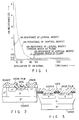
- FIG. 2 illustrates an example of the lateral MOSFET wherein electrodes are formed on the surface side of a substrate to cause current to flow in the element surface direction
- FIG. 3 does an example of the vertical MOSFET wherein one of main electrodes is formed on the undersurface side of the substrate to cause current to flow in the element vertical direction. Since the structures of the lateral and vertical MOSFETs are well-known, their detailed descriptions are omitted.
- the first advantage of the lateral MOSFET used as a switching element is as follows.
- the lateral MOSFET differs from the vertical MOSFET in time dependence of on-resistance for several hundreds of nanoseconds after an on-signal is supplied to a gate. While the on-resistance increases within a range from zero hertz to several megahertz in the vertical MOSFET, it decreases within the same range in the lateral MOSFET.
- the on-resistance of the vertical MOSFET continues to be higher than that (0.2 ⁇ ) of the vertical MOSFET through which a direct current flows, until the elapsed time t reaches 80 nsec and its average is approximately 1 ⁇ .
- the on-resistance of the lateral MOSFET is approximately 0.1 ⁇ which is lower than that (0.5 ⁇ ) of the lateral MOSFET through which a direct current flows, before the elapsed time t reaches 10 nsec.
- the switching loss can be reduced to approximately one-tenth within a frequency band of MHz.
- the on-resistance of the lateral MOSFET be lower than that of the MOSFET through which a direct current flows, when elapsed time t is 30 nsec, favorably 10 nsec.
- Such a lateral MOSFET is designed to meet the switching conditions that the switching frequency is 1 or higher (MHz) and the on-resistance is 1 or lower ( ⁇ /area of gate electrode).
- the second advantage of the lateral MOSFET is as follows.
- the input capacity C iss , output capacity C oss , and feedback capacity C rss of the lateral MOSFET which cause a switching loss, are approximately 1/10 as small as those of the vertical MOSFET.
- While the input capacity C iss of the vertical MOSFET ranges from 100 to 1000 pF, that of the lateral MOSFET is smaller and ranges from 10 to 100 pF. Thus, the switching loss due to the input capacity C iss can be reduced to one-tenth in the lateral MOSFET.
- the switching loss due to the output capacity C oss and feedback capacity C rss corresponds to energy required for discharging when an on-signal is input, it is 1/2 ⁇ f ⁇ (C rss + C oss ) ⁇ V gson 2 .
- the gate-to-source voltage V gs is set to V gso when it is switched. Since C rss + C oss is almost proportionate to C iss , the switching loss due to the output capacity and feedback capacity can also be reduced to one-tenth.
- the lateral MOSFET can sufficiently reduce in switching loss even in a frequency band of MHz since the response of on-resistance is quick when the on-signal is supplied and the parasitic capacitance is small.
- the on-resistance loss of the vertical MOSFET is less than that of the lateral MOSFET when the frequency is 1 MHz or lower. If, however, the frequency exceeds 1 MHz, the on-resistance loss of the lateral MOSFET becomes smaller than that of the vertical MOSFET. When the frequency is approximately 1 MHz, the on-resistance loss is 225 mW level.
- the total loss of the vertical MOSFET is less than that of the lateral MOSFET when the frequency is the vicinity of 500 KHz or lower. If, however, it exceeds the vicinity of 500 KHz, the total loss of the lateral MOSFET becomes smaller than that of the vertical MOSFET. When the frequency is the vicinity of 500KHz, the total loss is 250 mW level.
- a micro power supply device using a switching element according to each of the embodiments of the present invention will now be described in detail.
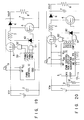
- FIG. 7 shows a micro power supply device using a switching element according to a first embodiment of the present invention.
- This micro power supply device is a switching power supply device comprising a chopper and a controller.
- the chopper includes a DC power supply, a switching element, an inductor, a transformer, a rectifier circuit, a smoother circuit, etc., and the controller does a feedback circuit, a PWM controller circuit, etc.
- the switching power supply device shown in FIG. 7 is a step-up DC/DC converter which receives a voltage from an input DC power supply 1 and boosts and stabilizes the voltage to output a DC voltage.
- the input DC power supply is, for example, a battery.
- a stabilizing capacitor 2 is connected in parallel to the input DC power supply 1 to stabilize an input voltage V in supplied from the power supply 1, and a lateral N-channel MOSFET (hereinafter referred to as FET) 4 serving as a switching element is connected to the input DC power supply 1 through an inductance 3.
- FET lateral N-channel MOSFET
- the FET 4 is turned (switched) on/off in response to a control signal from a pulse width modulation control IC (hereinafter referred to as PWM control IC) 5.
- PWM control IC pulse width modulation control IC
- the voltages generated at both ends of the FET 4 by switching of the FET 4, are rectified and smoothed by a rectifying diode 6 and a smoothing capacitor 7, respectively, in other words, they are converted into a DC voltage.
- the DC voltage is then supplied as an output voltage V out to a load 8 including, e.g., a portable telephone or another electronic apparatus.
- the output voltage V out is fed back to the PWM control IC 5 via a variable resistor 9.
- the PWM control IC 5 is integrated for the purpose of miniaturizing the micro power supply device and increasing its operation.
- Capacitors 10 and 11 and resistor 12 are connected to the IC 5 as external elements.
- the FET 4 is switched or turned on/off in response to a pulse width modulation signal supplied to a gate thereof from the PWM control IC 5. While the FET 4 is in an on-state, a current flows from the input DC power supply 1 to the inductor 3, and energy is accumulated therein. When the FET 4 is turned off, the energy is emitted from the inductor 3 to the load 8 through the diode 6. The DC voltage is always applied to the load 8 by the smoothing operation of the capacitor 7.
- the output voltage applied to the load 8 is fed back to the PWM control IC 5 via the variable resistor 9, and the IC 5 varies the waveform (duty ratio) of a pulse width modulated signal in order to fix the fed-back output voltage V out or minimize a difference between the output voltage V out and reference voltage. If the output voltage V out is higher than the reference voltage, the duty ratio of the PMW modulated signal and the energy accumulated in the inductor 3 is reduced. On the other hand, when the output voltage V out is lower than the reference voltage, the duty ratio is increased and so is the energy. Thus, the load 8 is supplied with the stabilized and boosted output voltage V out based on the input voltage V in from the input DC power supply 1.
- the FET 4 is driven at a gate potential of several tens of nanoseconds. If the FET 4 is turned on/off by control of pulse width or in response to the pulse width modulated signal in view of variations in the load 8, it is necessary that the duty ratio of the pulse width modulated signal be set to zero when the no load is applied and maximized when the maximum load is applied.
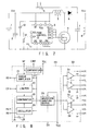
- FIG. 8 is a circuit diagram specifically showing the PWM control IC 5 of the micro power supply device of FIG. 7.
- the PWM control IC 5 includes a pulse width modulated signal generation circuit section 20 and a drive circuit section 30 for amplifying a pulse width modulated signal and turning on/off the FET 4.
- the comparator 23 produces a signal whose level becomes high during which period the triangular wave signal exceeds the level of output signal of the limiter 22 and whose level becomes low during the other period, in other words, the comparator 23 does a pulse width modulated signal whose duty ratio varies with the error voltage.
- the pulse width modulated signal is shaped into a correct rectangular wave by a waveform shaping device 26 and output from the pulse width modulated signal generation circuit section 20.
- the drive circuit section 30 includes a plurality of (four in this embodiment) amplifiers 31 to 34 which are arranged in parallel.
- the pulse width modulated signal is input from the section 20 is amplified by these amplifiers, and the amplified signals are output from respective four drive output terminals D1 to D4. As illustrated in FIG. 7, these drive output terminals D1 to D4 are connected in common outside the section 30, and the common connecting terminal is connected to the gate of the FET 4.
- Vcc is a power supply terminal which is connected to a positive terminal of the input DC power supply 1 shown in FIG. 7, and AG and PG are ground terminals which are connected to a negative terminal thereof.
- a comparator 27 is designed to compare an output voltage V out fed back to the feedback input terminal NF and a power supply input voltage applied to the power supply terminal Vcc (i.e., input voltage V in supplied from the input DC power supply 1) to supply a high-level signal to a comparison output terminal CMP when V in ⁇ V out and a low-level signal when V in > V out .
- This comparator 27 is employed in another embodiment described later.
- the comparison output terminal CMP is not shown in FIG. 7 since it is not used in the first embodiment.
- the FET 4 Since the FET 4 has to be turned on/off within a frequency band of MHz, a quick response is particularly required for the drive circuit section 30 of the PWM control IC 5. It is thus desirable to achieve the PWM control IC 5 using a Bi-CMOS of quick response. For this reason, the micro power supply device shown in FIG. 7 is constituted by a Bi-CMOSIC or a Bi-CMOSLSI. Another advantage of the lateral MOSFET is that it is simpler to mount the lateral MOSFET on one chip together with the PWM control IC 5 than the vertical MOSFET. This simple mounting is advantageous to a decrease in size and cost of the device.
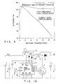
- FIG. 9 shows variations in efficiency (output voltage/input voltage ⁇ 100%) of the power supply device of FIG. 7, comparing the first embodiment using the FET 4 as a lateral MOSFET and an example using a vertical MOSFET.
- the switching frequency of the FET 4 is varied from 1 MHz to 11 MHz while the input voltage V in applied from the input DC power supply is 3.6 V and the output voltage V out applied to the load 8 is 5 V.
- the efficiency starts to decrease when the frequency exceeds 1 MHz and greatly lowers below 80% when the frequency is several megahertz (MHz).
- the efficiency of 80% or more is attained when the frequency ranges from 1 MHz to 11 MHz. Comparing both of them, the efficiency of the first embodiment is 13% higher than that of the example at the frequency of 5 MHz and it is 34% higher at the frequency of 10 MHz.
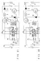
- FIG. 10 is a circuit diagram of a micro power supply device using a switching element according to a second embodiment of the present invention.
- This micro power supply device is a step-up DC/DC converter applicable to a low input voltage.
- the second embodiment differs from the first embodiment in that a power supply voltage selection circuit 13 is added.
- the power supply voltage selection circuit 13 is a circuit for selecting a higher one of an input voltage V in applied from the input DC power supply 1 and an output voltage V out applied to the load 8, as a power supply voltage applied to the power supply terminal VCC of the drive circuit section 30 shown in FIG. 8.
- the circuit 13 includes a diode 14a whose anode is connected to the positive terminal of the input DC power supply 1 and a diode 14b whose anode is connected to one end of the load 8.
- the cathodes of the diodes 14a and 14b are connected to the power supply terminal VCC.
- the device can stably be operated with high efficiency even when the input voltage V in applied from the input DC power supply 1 does not reach V th + V ds (V th : threshold voltage, V ds : drain-to-source voltage), the device can stably be operated with high efficiency.
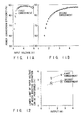
- FIGS. 11A and 11B show the dependence of power conversion efficiency upon input voltage in each of the first and second embodiments.
- the power supply voltage selection circuit 13 is operated to select a higher one of input and output voltages V in and V out and apply it to the drive circuit section 30 as an input power supply voltage, if a step-up operation is started, the output voltage V out is applied even though the input voltage V in does not reach V th + V ds . Therefore, a voltage of 5 V can be output from the power supply device of the second embodiment.
- FIG. 12 shows the dependence of the lower limit of input voltage V in upon output voltage with respect to each of the first and second embodiments, respectively.
- the lower limit of the input voltage at which the step-up operation can be performed rises as the output voltage increases. It is however seen that the step-up operation of the second embodiment is started at a voltage which is 0.6 V lower than that in the first embodiment, irrespective of the lower limit of the input voltage.
- the power supply voltage selection circuit selects a higher one of the input and output voltages V in and V out as a power supply voltage applied to the drive circuit section 30. If, however, the input and output voltages each have at least the minimum value necessary for operating the FET 4 in the linearity region, both of them can be used as a power supply voltage applied to the drive circuit section 30.
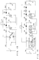
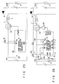
- FIG. 13 is a circuit diagram showing a micro power supply device using a switching element according to a third embodiment of the present invention.
- This micro power supply device is a step-up DC/DC converter having two cascade-connected chopper circuits for increasing in step-up ratio.
- the first chopper circuit includes an inductor 3a, an FET 4a, a diode 5a and a capacitor 6a, while the second chopper circuit does an inductor 3b, an FET 4b, a diode 5b and a capacitor 6b.
- the output voltage V out can be controlled by a variable resistor 9.
- the efficiency of 55% is attained.
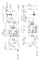
- FIG. 14 is a circuit diagram showing a micro power supply device using a switching element according to a fourth embodiment of the present invention.
- the device is so formed that a resonance operation is partially carried out.
- Inductors 3b and 3c constitute an output transformer. The objective of the transformer will be attained unless its coupling coefficient is -1, and the inductors 3a and 3b can be independent of each other.
- Each of FET sections 4a and 4b includes a plurality of lateral MOSFETs (two or three lateral MOSFETs in FIG. 14).
- the efficiency of 60 % can be obtained under the same conditions as those of the third embodiment.
- the FET sections 4a and 4b filled with the same charges as those of the capacities C rss and C oss are discharged. If, however, the resonance operation is performed as in the fourth embodiment, the discharge can be avoided thereby to improve in efficiency.
- FIG. 15 is a circuit diagram showing a micro power supply device using a switching element according to a fifth embodiment of the present invention.
- a charge pump circuit 15 having a double step-up ratio is used as a rectification smoothing circuit.
- the charge pump circuit 15 includes a plurality of diodes 15A and a plurality of capacitors 15B.
- the input voltage V in applied from the input DC power supply 1 is 5 V, while the output voltage is 20 V and 40 V.
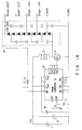
- FIG. 16 is a circuit diagram showing a micro power supply device using a switching element according to a sixth embodiment of the present invention.
- a charge pump circuit 16 is used, but its step-up ratio is set such that the circuit 16 outputs a double to quintuple voltage.
- the charge pump circuit 16 includes a plurality of diodes 16A and a plurality of capacitors 16B.
- the input voltage V in applied from the input DC power supply 1 is 5 V, while the output voltage V out may exceed 100 V.
- FIG. 17 is a circuit diagram showing a micro power supply device using a switching element according to a seventh embodiment of the present invention, and the device is a step-down DC/DC converter. As illustrated in FIG. 17, a lateral PMOSFET 41 and an inductor 3 are connected in series between the input DC power supply 1 and load 8, and the connection of a rectifying diode 42 is changed accordingly.
- a PMOSFET is employed in the FET 41, the polarity of a pulse width modulated signal is inverted.
- a PWM control IC 43 shown in FIG. 17 has inversion output terminals /D1 to /D4 corresponding to the drive output terminals D1 to D4.
- the output voltage V out can be controlled by a variable resistor 9.
- the input voltage V in applied from the input DC power supply 1 is 5 to 20 V, while the output voltage V out is 6.5 V and the output is 1 W.
- efficiency of 85% can be obtained.
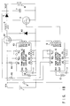
- FIG. 18 is a circuit diagram showing a micro power supply device using a switching element according to an eighth embodiment of the present invention.
- the device is a step-up/step-down DC/DC converter capable of both step-up and step-down operations, and constituted by combining the step-up DC/DC converter of FIG. 1 and the step-down DC/DC converter of FIG. 7, as illustrated in FIG. 18.
- PWM control ICs 5 and 43 are provided for the respective converters.
- the PWM control IC5 used for the step-up converter for turning on/off an NMOSFET 4 and the PWM control IC 43 used for the step-down converter for turning on/off a PMOSFET 41 are provided with master and slave sync terminals M and S, respectively. By connecting these terminals, both the PWM control ICs 5 and 43 are synchronized with each other.
- the NMOSFET 4 is subjected to ON-ON control and the PMOSFET 41 is always rendered in an OFF-state to serve as a step-up DC/DC converter.
- FIG. 19 is a circuit diagram showing a micro power supply device using a switching element according to a ninth embodiment of the present invention.
- This device includes a PWM control IC 50 having both functions of the step-up converter PWM control IC5 and step-down converter PWM control IC 43 shown in FIG. 18.
- a terminal PWM of the PWM control IC 50 corresponds to a set of the drive output terminals D1 to D4 described above, a terminal CMP thereof is an output terminal for outputting a signal compared by the comparator 27 shown in FIG. 8, and a terminal /CMP is an output terminal for outputting an inverted signal thereof.
- the output signals of the terminals PWM and CPM are supplied to a gate circuit 51, and the output signal of the gate circuit 51 is input to the gate of the NMOSFET 4. Moreover, the output signals of the terminals PWM and /CMP are supplied to a gate circuit 52, and the output signal of the gate circuit 52 is input to the gate of the PMOSFET 41.
- the terminal /CMP is provided to always turn on the step-down PMOSFET 41 in the step-up operation
- the terminal CMP is done to always turn off the step-up NMOSFET 4 in the step-down operation.
- the PMOSFET 41 is always turned on and the NMOSFET 4 is turned on and turned off in accordance with the high and low levels of terminal PWM, respectively, thus performing a step-up operation.
- the NMOSFET 4 When the levels of terminals CMP and /CMP are low and high, respectively, the NMOSFET 4 is always turned off and the PMOSFET 41 is turned on and turned off in accordance with the low and high levels of terminal PWM, respectively, thus performing a step-down operation.
- FIG. 20 is a circuit diagram showing a micro power supply device using a switching element according to a tenth embodiment of the present invention.
- this device the same function as that of the device shown in FIG. 19 is fulfilled by combining a PWM control IC 4 for a step-up converter with gate circuits 61 and 62.
- FIG. 21 is a circuit diagram showing a micro power supply device using a switching element according to an eleventh embodiment of the present invention.
- the same function as that of the device shown in FIG. 19 is performed by combining a PWM control IC 43 for a step-down converter with gate circuits 71 and 72.
- FIG. 22 is a circuit diagram showing a micro power supply device using a switching element according to a twelfth embodiment of the present invention.
- the same function as that of the device shown in FIG. 19 is fulfilled by using a PWM control IC 81 for a step-up/step-down converter in which drive output terminals D3 and D4 are replaced with inversion output terminals /D3 and /D4, in other words, by incorporating the functions of the gate circuits 51 and 52 shown in FIG. 19 into the PWM control IC 81.
- FIG. 23 is a circuit diagram showing a micro power supply device using a switching element according to a thirteenth embodiment of the present invention.
- This device comprises a PWM control IC 82 for a step-up/step-down converter into which the FETs 4 and 41 and diodes 6 and 42 shown in FIG. 22 are incorporated.
- the external elements are only L, C and R and thus the number of elements is greatly reduced, the device can be decreased in size, weight and cost.
- FIG. 24 is a circuit diagram showing a micro power supply device using a switching element according to a fourteenth embodiment of the present invention.
- an inversion DC/DC converter is constituted by changing the positions of inductor 3 and diode 42 shown in FIG. 17 to each other.
- a feedback input terminal NF senses the current to be drawn out since its polarity is negative.
- FIG. 25 is a circuit diagram showing a micro power supply device using a switching element according to a fifteenth embodiment of the present invention.
- an inversion DC/DC converter is constituted by combining a PWM control IC 90 for an inversion converter and gate circuits 91 and 92.
- FIG. 26 is a circuit diagram showing a micro power supply device using a switching element according to a sixteenth embodiment of the present invention.
- a PWM control IC 5 for a step-up converter is used as in the tenth embodiment shown in FIG. 20, and an inversion DC/DC converter is constituted by combining the IC 5 with a gate circuit 62.
- reference numerals 100 and 101 indicate a transistor and a resistor, respectively, which are incorporated into a feedback circuit.
- a micro power supply device using a switching element which can be operated with high efficiency by considerably reducing a switching loss even within a switching frequency band of MHz.
- a micro power supply device using a switching element which can stably be operated with high efficiency by operating a MOSFET within a linearity region even if an input voltage applied from an input DC power supply is dropped.
Landscapes
- Engineering & Computer Science (AREA)
- Power Engineering (AREA)
- Dc-Dc Converters (AREA)
Claims (17)
- Un dispositif de micro-alimentation utilisant un élément de commutation qui comporte une section de découpage (3, 4, 6, 7, 15) pour commuter une tension de sortie d'une alimentation à courant continu et une section de commande (5, 13) pour appliquer un signal de commande de commutation à la section de découpage (3, 4, 6, 7, 15) en réponse à la tension de sortie de la section de découpage,
caractérisé en ce que la section de découpage (3, 4, 6, 7, 15) comprend :un MOSFET latéral (4);un élément de redressement (6) pour redresser la tension de sortie qui est commutée par le MOSFET latéral (4); etun élément à inductance (3) connecté à au moins un élément parmi le MOSFET latéral (4) et l'élément de redressement (6). - Le dispositif de micro-alimentation selon la revendication 1, caractérisé en ce que la section de commande (5, 13) comprend :des moyens de génération de signal (5) pour générer le signal de commande de commutation;des moyens d'attaque (5) pour amplifier le signal de commande de commutation qui est généré par les moyens de génération de signal (5) et pour attaquer le MOSFET latéral (4); etdes moyens de sélection (13) pour sélectionner une tension parmi la tension de sortie de l'alimentation à courant continu et la tension de sortie de la section de redressement (6), à titre de tension d'alimentation appliquée aux moyens d'attaque (5), la tension qui est sélectionnée, parmi les deux tensions de sortie, n'étant pas inférieure à une valeur minimale nécessaire pour faire fonctionner le MOSFET latéral (4) dans une région linéaire.
- Le dispositif de micro-alimentation selon l'une quelconque des revendications précédentes, caractérisé en ce que la section de commande (5, 13) comprend :des moyens de génération de signal (5) pour générer le signal de commande de commutation;des moyens d'attaque (5) pour amplifier le signal de commande de commutation qui est généré par les moyens de génération de signal (5) et pour attaquer le MOSFET latéral (4); etdes moyens de sélection (13) pour sélectionner la tension la plus élevée parmi la tension de sortie de l'alimentation à courant continu et la tension de sortie de la section de redressement (6), à titre de tension d'alimentation appliquée aux moyens d'attaque (5).
- Le dispositif de micro-alimentation selon l'une quelconque des revendications précédentes, caractérisé en ce que le MOSFET latéral (4) a une caractéristique telle que lorsqu'un signal de conduction est fourni à partir des moyens de commande (5) sous la forme d'un signal en modulation d'impulsions en largeur, la résistance à l'état conducteur devient inférieure à la résistance en courant continu en une durée ne dépassant pas 30 nanosecondes.
- Le dispositif de micro-alimentation selon l'une quelconque des revendications précédentes, caractérisé en ce que la section de commande (5, 13) comprend des moyens pour effectuer une commande par MIL du MOSFET latéral (4) à une fréquence de commutation de 1 MHz ou plus.
- Le dispositif de micro-alimentation selon l'une quelconque des revendications précédentes, caractérisé en ce que le MOSFET latéral (4) de la section de découpage (3, 4, 6, 7, 15) et la section de commande (5) sont formés sur une seule puce.
- Le dispositif de micro-alimentation selon l'une quelconque des revendications précédentes, caractérisé en ce que la section de découpage (3, 4, 6, 7, 15) comprend un ensemble de circuits de découpage connectés en cascade, et chacun de cet ensemble de circuits de découpage (3a, 4a, 6a, 7a, 3b, 4b, 6b, 7b) comprend :un MOSFET latéral (4);un élément de redressement (6) pour redresser la tension de sortie qui est commutée par le MOSFET latéral (4); etun élément à inductance (3) connecté à au moins un élément parmi le MOSFET latéral (4) et l'élément de redressement (6).
- Le dispositif de micro-alimentation selon la revendication 7, caractérisé en ce que la section de découpage (3, 4, 6, 7, 15) comprend un circuit résonnant (3a, 3b, 3c, 7a) connecté entre les circuits de découpage (3a, 4a, 6a, 7a, 3b, 4b, 6b, 7b).
- Le dispositif de micro-alimentation selon l'une quelconque des revendications précédentes, caractérisé en ce que l'élément de redressement (6) de la section de découpage (3, 4, 6, 7, 15) comprend un circuit de pompe de charge (15) pour augmenter la tension de sortie de l'élément de redressement (6).
- Le dispositif de micro-alimentation selon l'une quelconque des revendications précédentes, caractérisé en ce que la section de découpage (3, 4, 6, 7, 15) comprend un convertisseur continu/continu élévateur.
- Le dispositif de micro-alimentation selon l'une quelconque des revendications 1 à 9, caractérisé en ce que la section de découpage (3, 4, 6, 7, 15) comprend un convertisseur continu/continu abaisseur.
- Le dispositif de micro-alimentation selon l'une quelconque des revendications 1 à 9, caractérisé en ce que la section de découpage (3, 4, 6, 7, 15) comprend un convertisseur continu/continu élévateur et un convertisseur continu/continu abaisseur, et des moyens pour activer sélectivement l'un des convertisseurs.
- Le dispositif de micro-alimentation selon la revendication 12, caractérisé en ce que la section de découpage (3, 4, 6, 7, 15) comprend une section de commande qui comprend également des sections de commande intégrées pour le convertisseur continu/continu élévateur et le convertisseur continu/continu abaisseur.
- Un dispositif de micro-alimentation selon la revendication 1, caractérisé en outre en ce que la section de commande (5) comprend des moyens de sélection (15) pour fournir sélectivement la tension de sortie de l'alimentation à courant continu ou la tension de sortie de la section de redressement, à titre de tension d'alimentation de la section de commande (5).
- Le dispositif de micro-alimentation selon la revendication 14, caractérisé en ce que la tension de sortie sélectionnée n'est pas inférieure à une valeur minimale nécessaire pour faire fonctionner l'élément de commutation à semiconducteurs (4) dans une région linéaire.
- Le dispositif de micro-alimentation selon la revendication 14, caractérisé en ce que les moyens de sélection (15) comprennent des moyens pour sélectionner la tension la plus élevée parmi la tension de sortie de l'alimentation à courant continu et la tension de sortie de la section de redressement (6), à titre de tension d'alimentation appliquée à la section de commande (5).
- Un dispositif de micro-alimentation selon la revendication 1, dans lequel la structure est telle que la tension de sortie de l'alimentation à courant continu peut être commutée à une fréquence de commutation d'au moins 1 MHz, et avec une résistivité à l'état conducteur de 1 Ω/mm2 ou moins.
Applications Claiming Priority (2)
| Application Number | Priority Date | Filing Date | Title |
|---|---|---|---|
| JP222244/94 | 1994-09-16 | ||
| JP22224494 | 1994-09-16 |
Publications (2)
| Publication Number | Publication Date |
|---|---|
| EP0702449A1 EP0702449A1 (fr) | 1996-03-20 |
| EP0702449B1 true EP0702449B1 (fr) | 1998-04-01 |
Family
ID=16779363
Family Applications (1)
| Application Number | Title | Priority Date | Filing Date |
|---|---|---|---|
| EP95306443A Expired - Lifetime EP0702449B1 (fr) | 1994-09-16 | 1995-09-14 | Micro-alimentation de puissance avec un élément interrupteur |
Country Status (4)
| Country | Link |
|---|---|
| US (1) | US5677617A (fr) |
| EP (1) | EP0702449B1 (fr) |
| KR (1) | KR100201430B1 (fr) |
| DE (1) | DE69501931T2 (fr) |
Cited By (1)
| Publication number | Priority date | Publication date | Assignee | Title |
|---|---|---|---|---|
| CN106464137A (zh) * | 2014-05-29 | 2017-02-22 | 索尼互动娱乐股份有限公司 | 开关转换器和使用该开关转换器的电子设备 |
Families Citing this family (23)
| Publication number | Priority date | Publication date | Assignee | Title |
|---|---|---|---|---|
| FR2744299B1 (fr) * | 1996-01-26 | 1998-04-30 | Sgs Thomson Microelectronics | Convertisseur continu/continu a faible tension d'alimentation |
| JPH09266666A (ja) * | 1996-03-28 | 1997-10-07 | Rohm Co Ltd | 昇圧回路とその制御回路 |
| US5982156A (en) * | 1997-04-15 | 1999-11-09 | The United States Of America As Represented By The Secretary Of The Air Force | Feed-forward control of aircraft bus dc boost converter |
| US5949275A (en) * | 1997-05-02 | 1999-09-07 | Delco Electronics Corp. | Dual output voltage boost circuit |
| JP3148171B2 (ja) * | 1998-01-12 | 2001-03-19 | 株式会社日本プロテクター | スイッチングレギュレータ |
| US6115272A (en) * | 1998-10-26 | 2000-09-05 | Waferscale Integration, Inc. | Duty cycle based charge pump controller |
| JP2001094094A (ja) | 1999-09-21 | 2001-04-06 | Hitachi Ltd | 半導体装置およびその製造方法 |
| US7280014B2 (en) | 2001-03-13 | 2007-10-09 | Rochester Institute Of Technology | Micro-electro-mechanical switch and a method of using and making thereof |
| WO2002097865A2 (fr) | 2001-05-31 | 2002-12-05 | Rochester Institute Of Technology | Soupapes, agitateurs et pompes microfluidiques et procedes correspondants |
| TW571494B (en) * | 2001-06-05 | 2004-01-11 | Us Microbattery Inc | Micro power supply with integrated charging capability |
| US7211923B2 (en) | 2001-10-26 | 2007-05-01 | Nth Tech Corporation | Rotational motion based, electrostatic power source and methods thereof |
| US7378775B2 (en) | 2001-10-26 | 2008-05-27 | Nth Tech Corporation | Motion based, electrostatic power source and methods thereof |
| US6750590B2 (en) * | 2001-10-26 | 2004-06-15 | Nth Tech Corporation | Electrostatic based power source and method thereof |
| US7400121B2 (en) * | 2002-08-06 | 2008-07-15 | Texas Instruments Incorporated | Soft-start system for voltage regulator and method of implementing soft-start |
| TWI246821B (en) * | 2002-12-25 | 2006-01-01 | Rohm Co Ltd | Parallel operation system for dc-ac converting device and its controller IC |
| JP3708088B2 (ja) * | 2003-03-28 | 2005-10-19 | Tdk株式会社 | スイッチング電源の出力制御方法、出力制御回路およびスイッチング電源 |
| US7217582B2 (en) | 2003-08-29 | 2007-05-15 | Rochester Institute Of Technology | Method for non-damaging charge injection and a system thereof |
| US7287328B2 (en) | 2003-08-29 | 2007-10-30 | Rochester Institute Of Technology | Methods for distributed electrode injection |
| US8581308B2 (en) | 2004-02-19 | 2013-11-12 | Rochester Institute Of Technology | High temperature embedded charge devices and methods thereof |
| US8099619B2 (en) * | 2006-09-28 | 2012-01-17 | Intel Corporation | Voltage regulator with drive override |
| JP5386246B2 (ja) | 2009-06-26 | 2014-01-15 | パナソニック株式会社 | 電力変換装置 |
| JP5709275B2 (ja) * | 2012-12-19 | 2015-04-30 | シオン電機株式会社 | 電力送出システム |
| DE102017107070A1 (de) | 2017-04-03 | 2018-10-04 | AccuPower Forschungs-, Entwicklungs- und Vertriebsgesellschaft mbH | Kaskadierbare anordnung zum verschalten einer vielzahl von energiespeichern sowie verfahren zur steuerung der energieversorgung bei diesen energiespeichern |
Family Cites Families (3)
| Publication number | Priority date | Publication date | Assignee | Title |
|---|---|---|---|---|
| US4720668A (en) * | 1986-06-20 | 1988-01-19 | Lee Fred C | Zero-voltage switching quasi-resonant converters |
| NL8601774A (nl) * | 1986-07-08 | 1988-02-01 | Philips Nv | Dc-voedingsinrichting voor een telecommunicatieleiding. |
| FR2707051B1 (fr) * | 1993-06-10 | 1996-03-08 | Matsushita Electric Works Ltd |
-
1995
- 1995-09-14 US US08/528,014 patent/US5677617A/en not_active Expired - Lifetime
- 1995-09-14 EP EP95306443A patent/EP0702449B1/fr not_active Expired - Lifetime
- 1995-09-14 DE DE69501931T patent/DE69501931T2/de not_active Expired - Lifetime
- 1995-09-16 KR KR1019950030355A patent/KR100201430B1/ko not_active Expired - Fee Related
Cited By (2)
| Publication number | Priority date | Publication date | Assignee | Title |
|---|---|---|---|---|
| CN106464137A (zh) * | 2014-05-29 | 2017-02-22 | 索尼互动娱乐股份有限公司 | 开关转换器和使用该开关转换器的电子设备 |
| CN106464137B (zh) * | 2014-05-29 | 2020-02-21 | 索尼互动娱乐股份有限公司 | 开关转换器和使用该开关转换器的电子设备 |
Also Published As
| Publication number | Publication date |
|---|---|
| DE69501931T2 (de) | 1998-09-10 |
| KR960012676A (ko) | 1996-04-20 |
| EP0702449A1 (fr) | 1996-03-20 |
| DE69501931D1 (de) | 1998-05-07 |
| KR100201430B1 (ko) | 1999-06-15 |
| US5677617A (en) | 1997-10-14 |
Similar Documents
| Publication | Publication Date | Title |
|---|---|---|
| US5677617A (en) | Micro power supply device using switching element | |
| US7345894B2 (en) | Cascode switch power supply | |
| US8207714B2 (en) | Method and apparatus for external control mode step down switching regulator | |
| US7548050B2 (en) | Switching power supply device and semiconductor integrated circuit | |
| US6920055B1 (en) | Charge pumping system and method | |
| JP3175227B2 (ja) | Dc/dc電圧変換装置 | |
| US8193793B2 (en) | DC-DC converter | |
| US7098639B2 (en) | DC-DC converter and method for controlling DC-DC converter | |
| US7262587B2 (en) | Circuit and method for controlling DC-DC converter | |
| US7847621B2 (en) | Control circuit and control method for charge pump circuit | |
| JP3475887B2 (ja) | スイッチング電源装置 | |
| US8193853B2 (en) | Efficiency and thermal improvement of a charge pump by mixing different input voltages | |
| KR100281862B1 (ko) | 전기 2중층 콘덴서를 사용하는 이차 전지 유니트 | |
| JPH06311736A (ja) | Dc/dcコンバータ | |
| US7202643B2 (en) | High efficiency DC-to-DC synchronous buck converter | |
| US20110001462A1 (en) | Electronic device and method for dc-dc conversion | |
| JP2004096816A (ja) | 多出力dc−dcコンバータ | |
| JPH08140341A (ja) | スイッチング素子を用いたマイクロ電源装置 | |
| US6437546B1 (en) | DC-to-DC converter and electronic device using the same | |
| US7453303B2 (en) | Control circuit for lossless switching converter | |
| CN119696350A (zh) | 一种开关电源的自供电电路及开关电源 | |
| KR100426606B1 (ko) | Dc ―dc 컨버터 및 이를 사용한 전자장치 | |
| JP2007501598A (ja) | 同期整流器の出力電圧制御 | |
| JP2001037214A (ja) | 電源回路 | |
| JP2003111394A (ja) | Dc−dcコンバータ |
Legal Events
| Date | Code | Title | Description |
|---|---|---|---|
| PUAI | Public reference made under article 153(3) epc to a published international application that has entered the european phase |
Free format text: ORIGINAL CODE: 0009012 |
|
| 17P | Request for examination filed |
Effective date: 19951011 |
|
| AK | Designated contracting states |
Kind code of ref document: A1 Designated state(s): DE FR |
|
| 17Q | First examination report despatched |
Effective date: 19960724 |
|
| GRAG | Despatch of communication of intention to grant |
Free format text: ORIGINAL CODE: EPIDOS AGRA |
|
| GRAG | Despatch of communication of intention to grant |
Free format text: ORIGINAL CODE: EPIDOS AGRA |
|
| GRAH | Despatch of communication of intention to grant a patent |
Free format text: ORIGINAL CODE: EPIDOS IGRA |
|
| GRAH | Despatch of communication of intention to grant a patent |
Free format text: ORIGINAL CODE: EPIDOS IGRA |
|
| GRAA | (expected) grant |
Free format text: ORIGINAL CODE: 0009210 |
|
| AK | Designated contracting states |
Kind code of ref document: B1 Designated state(s): DE FR |
|
| REF | Corresponds to: |
Ref document number: 69501931 Country of ref document: DE Date of ref document: 19980507 |
|
| ET | Fr: translation filed | ||
| PLBE | No opposition filed within time limit |
Free format text: ORIGINAL CODE: 0009261 |
|
| STAA | Information on the status of an ep patent application or granted ep patent |
Free format text: STATUS: NO OPPOSITION FILED WITHIN TIME LIMIT |
|
| 26N | No opposition filed | ||
| PGFP | Annual fee paid to national office [announced via postgrant information from national office to epo] |
Ref country code: DE Payment date: 20110907 Year of fee payment: 17 Ref country code: FR Payment date: 20110922 Year of fee payment: 17 |
|
| REG | Reference to a national code |
Ref country code: FR Ref legal event code: ST Effective date: 20130531 |
|
| REG | Reference to a national code |
Ref country code: DE Ref legal event code: R119 Ref document number: 69501931 Country of ref document: DE Effective date: 20130403 |
|
| PG25 | Lapsed in a contracting state [announced via postgrant information from national office to epo] |
Ref country code: DE Free format text: LAPSE BECAUSE OF NON-PAYMENT OF DUE FEES Effective date: 20130403 |
|
| PG25 | Lapsed in a contracting state [announced via postgrant information from national office to epo] |
Ref country code: FR Free format text: LAPSE BECAUSE OF NON-PAYMENT OF DUE FEES Effective date: 20121001 |