EP0703052A1 - Spritzgiessform für IC-Karten - Google Patents
Spritzgiessform für IC-Karten Download PDFInfo
- Publication number
- EP0703052A1 EP0703052A1 EP95114822A EP95114822A EP0703052A1 EP 0703052 A1 EP0703052 A1 EP 0703052A1 EP 95114822 A EP95114822 A EP 95114822A EP 95114822 A EP95114822 A EP 95114822A EP 0703052 A1 EP0703052 A1 EP 0703052A1
- Authority
- EP
- European Patent Office
- Prior art keywords
- cavity
- sprue
- card
- gate
- mold
- Prior art date
- Legal status (The legal status is an assumption and is not a legal conclusion. Google has not performed a legal analysis and makes no representation as to the accuracy of the status listed.)
- Withdrawn
Links
Images


Classifications
-
- G—PHYSICS
- G06—COMPUTING OR CALCULATING; COUNTING
- G06K—GRAPHICAL DATA READING; PRESENTATION OF DATA; RECORD CARRIERS; HANDLING RECORD CARRIERS
- G06K19/00—Record carriers for use with machines and with at least a part designed to carry digital markings
- G06K19/06—Record carriers for use with machines and with at least a part designed to carry digital markings characterised by the kind of the digital marking, e.g. shape, nature, code
- G06K19/067—Record carriers with conductive marks, printed circuits or semiconductor circuit elements, e.g. credit or identity cards also with resonating or responding marks without active components
- G06K19/07—Record carriers with conductive marks, printed circuits or semiconductor circuit elements, e.g. credit or identity cards also with resonating or responding marks without active components with integrated circuit chips
- G06K19/077—Constructional details, e.g. mounting of circuits in the carrier
- G06K19/0772—Physical layout of the record carrier
- G06K19/07724—Physical layout of the record carrier the record carrier being at least partially made by a molding process
-
- B—PERFORMING OPERATIONS; TRANSPORTING
- B29—WORKING OF PLASTICS; WORKING OF SUBSTANCES IN A PLASTIC STATE IN GENERAL
- B29C—SHAPING OR JOINING OF PLASTICS; SHAPING OF MATERIAL IN A PLASTIC STATE, NOT OTHERWISE PROVIDED FOR; AFTER-TREATMENT OF THE SHAPED PRODUCTS, e.g. REPAIRING
- B29C45/00—Injection moulding, i.e. forcing the required volume of moulding material through a nozzle into a closed mould; Apparatus therefor
- B29C45/0025—Preventing defects on the moulded article, e.g. weld lines, shrinkage marks
-
- B—PERFORMING OPERATIONS; TRANSPORTING
- B29—WORKING OF PLASTICS; WORKING OF SUBSTANCES IN A PLASTIC STATE IN GENERAL
- B29C—SHAPING OR JOINING OF PLASTICS; SHAPING OF MATERIAL IN A PLASTIC STATE, NOT OTHERWISE PROVIDED FOR; AFTER-TREATMENT OF THE SHAPED PRODUCTS, e.g. REPAIRING
- B29C45/00—Injection moulding, i.e. forcing the required volume of moulding material through a nozzle into a closed mould; Apparatus therefor
- B29C45/17—Component parts, details or accessories; Auxiliary operations
- B29C45/26—Moulds
- B29C45/27—Sprue channels ; Runner channels or runner nozzles
- B29C45/2701—Details not specific to hot or cold runner channels
-
- G—PHYSICS
- G06—COMPUTING OR CALCULATING; COUNTING
- G06K—GRAPHICAL DATA READING; PRESENTATION OF DATA; RECORD CARRIERS; HANDLING RECORD CARRIERS
- G06K19/00—Record carriers for use with machines and with at least a part designed to carry digital markings
- G06K19/06—Record carriers for use with machines and with at least a part designed to carry digital markings characterised by the kind of the digital marking, e.g. shape, nature, code
- G06K19/067—Record carriers with conductive marks, printed circuits or semiconductor circuit elements, e.g. credit or identity cards also with resonating or responding marks without active components
- G06K19/07—Record carriers with conductive marks, printed circuits or semiconductor circuit elements, e.g. credit or identity cards also with resonating or responding marks without active components with integrated circuit chips
- G06K19/077—Constructional details, e.g. mounting of circuits in the carrier
- G06K19/07745—Mounting details of integrated circuit chips
-
- B—PERFORMING OPERATIONS; TRANSPORTING
- B29—WORKING OF PLASTICS; WORKING OF SUBSTANCES IN A PLASTIC STATE IN GENERAL
- B29L—INDEXING SCHEME ASSOCIATED WITH SUBCLASS B29C, RELATING TO PARTICULAR ARTICLES
- B29L2017/00—Carriers for sound or information
- B29L2017/006—Memory cards, chip cards
Definitions
- the present invention relates to an injection mold for molding IC cards by an injection molding machine.
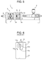
- Fig. 5 shows an injection molding machine 1 which comprises an injection unit 2 having a nozzle 2a, and a mold clamping mechanism 3.
- the mold clamping mechanism 3 comprises a fixed platen 3a, a movable platen 3b, a fixed mold 4 secured to the fixed platen 3a, and a movable mold 5 secured to the movable platen 3b.
- a hydraulic cylinder 6 is connected to the movable platen 3b through a toggle 7 so as to move the movable platen.
- Either of the fixed mold 4 or the movable mold 5 has a rectangular recess to form a cavity between the fixed mold and the movable mold when the movable mold 5 is engaged with the fixed mold 4 for molding an IC card.
- a projecting portion 16a (Fig. 2) is formed for forming a recess 10b (Fig. 6) in which a module of the IC card is engaged.
- a sprue is formed in the mold to be communicated with the cavity so that molten resin ejected from the nozzle 2a of the injection unit 2 is fed to the cavity passing through the sprue.
- the cylinder 6 is operated to move the movable platen 3b to the fixed platen 3a through the toggle 7 so that the movable mold 5 is engaged with the fixed mold 4.
- the nozzle 2a of the injection unit 2 is moved to engage with the fixed mold 4, and molten resin is ejected from the nozzle 2a and poured in the cavity through the sprue at a high pressure.
- a plastic IC card is molded in the cavity.
- the cylinder is operated so as to disengage the movable mold 5 from the fixed mold 4.
- the molded plastic IC card is removed from the cavity.
- the cavity is charged with the molten resin at a moment, so that an IC card having a high quality can be molded. Furthermore, since the residual of the molten resin in the sprue is reduced, thereby decreasing consumption of resin.
- the IC card is required to have a sufficient bending strength.
- a bending test has been conducted to bend the card about a longitudinal axis and a lateral axis.
- Fig. 6 shows a plastic IC card 10 molded in a cavity 13.
- the recess 10b is formed by the projecting portion 16a for mounting the IC module.
- a weld mark 10a is liable to be formed along a confluent line between opposite flows 10c and 10d divided by the projection portion 16a. Such a weld mark coincides with a longitudinal line of the card which is perpendicular to a lateral bending moment. Consequently, the card may be easily bent.
- Fig. 7 shows another conventional injection mold in which a pair of cavities 13 are provided in the mold.
- a runner 12 connected to a sprue (not shown) and having a pair of branch runners 12a is provided between the cavities 13.
- a gate 11 is provided on an end of each branch runner 12a to be communicated with the cavity 13 at an offset position.
- the resin When the molten resin is fed in the runner 12, the resin is turned at the branch runners 12a in the opposite directions and ejected from the respective gates 11 to the cavities 13.
- the ejected molten resin is distributed in the cavity 13 as shown by arrows, in a curve due to the runners bent at 90 degrees. Therefore, a right area of the cavity 13 in Fig. 7 is liable not to be charged with the resin. Accordingly, the IC card having a high quality is not molded.
- An object of the present invention is to provide an injection mold which may produce an IC card having a high quality.
- an injection mold for an IC card comprising a fixed mold, a movable mold, the fixed mold and the movable mold being provided to form a cavity having a projecting portion for forming a recess on an IC card to be molded, a sprue bush provided in the fixed mold to form a sprue therein, a gate for communicating the sprue with the cavity.
- a hole is formed in the fixed mold, which is communicated with the sprue and in which a nozzle of an injection molding machine is inserted.
- An interval of the cavity at a front portion near the gate is set to a thickness of the IC card, and an interval of the cavity at an end opposite to the gate is larger than the interval at the front portion.
- the gate is located at a position deviated from a position corresponding to the projecting portion.
- a runner is communicated with the sprue, and a branch runner is communicated with the runner and the gate.
- the branch runner makes 90 degrees with the runner.
- the gate is positioned near an interior end corner of a bottom line of the cavity.
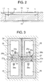
- FIG. 1 showing an injection mold of the present invention
- parts which are the same as the machine shown in Fig. 5 are identified with the same reference numerals as Fig. 5.
- the injection mold has a fixed mold assembly 14a and a movable mold assembly 15a.
- the fixed mold assembly 14a comprises a fixed mold 14, a backing plate 41 secured to the fixed mold 14, and a bottom plate 42 secured to the backing plate 41.
- the bottom plate 42 is attached to the fixed platen 3a of the mold clamping mechanism 3 (Fig. 5).
- the movable mold assembly 15a has a movable mold 15 secured to a backing plate 51 which is attached to the movable platen 3b.
- the movable mold 15 has a recess so as to form a cavity 16 between the molds 14 and 15.
- the backing plates 41 and 51 are provided for reinforcing the molds 14 and 15, respectively.
- a projecting portion 16a (Fig. 2) is provided for forming the recess 10b of the IC card 10 (Fig. 6).
- the bottom plate 42 has an opening 42a formed corresponding to the nozzle 2a of the injection unit 2.
- the backing plate 41 has a conical hole 41a having an inner cylindrical hole 41b corresponding to the opening 42a of the bottom plate 42.
- a hole 41c is formed in the backing plate 41 to be communicated with the inner hole 41b and communicated with a hole 41d in the fixed mold 14.
- a sprue bush 44 having a sprue 43 is inserted into the hole 41b and the holes 41c and 41d.
- a flange 44a of the sprue bush 44 is engaged with a base portion of the inner hole 41b and secured thereto with bolts.
- the flange 44a has a recess 44b to be engaged with an end of the nozzle 2a.
- An inner end of the sprue 43 is communicated with a gate 17 which is communicated with the cavity 16.
- the nozzle 2a is inserted into opening 42a and holes 41a and 41b and engaged with the recess 44b of the sprue bush 44.
- the nozzle ejects the molten resin to the sprue 43 from which the resin is fed to the cavity 16 through the gate 17.
- the bottom plate 42 and the backing plate 41 of the fixed mold 14 have the opening 42a and the holes 41a and 41b in which the nozzle 2a of the injection unit 2 is inserted. Therefore, even if the thickness of the mold is increased because of the bottom plate and the backing plate, the length of the sprue 43 can be reduced. Since the length of the sprue is shortened, the cavity is charged with the molten resin at a moment. Consequently, the IC card is molded with a high quality. Furthermore, the residual of the molten resin in the sprue is reduced to reduce the consumption of the resin.
- Fig. 2 shows the cavity 16 formed between the molds 14 and 15.
- the molded IC card has the thickness of 0.81 mm. Accordingly, the interval t1 of the cavity 16 near the gate 17 is set to 0.81 mm. However, the interval t2 at the end opposite to the gate is set to 0.83 mm which is larger than the thickness of the IC card.
- the IC card having a uniform thickness of 0.81 mm is not molded. It has been found that the thickness of the molded IC card is reduced to 0.79 mm at the interval t2 of the cavity.
- the depth of the cavity 16 is set in a different value in dependency on the position in the cavity with respect to the gate 17.
- the depth of the cavity at the interval t2 away from the gate is set larger than the thickness of the card for supplementing the thickness, thereby preventing the thickness from unequally reducing.
- FIG. 3 shows another embodiment of the present invention.
- a fixed mold 24 has four cavities 26 each of which has a projecting portion 26a.
- a sprue 21 is provided at a central portion of the mold.
- a pair of runners 22 are provided between upper and lower cavities 26 to be communicated with the sprue 21 in parallel with a bottom line 26c of the cavity 26.
- Each runner 22 has a pair of branch runners 22a provided at an end portion thereof to be symmetrically extended in the perpendicular directions toward the cavities.
- a gate 27 is provided on an end portion of the branch runner 22a to be communicated with the cavity 26, at a position downstream of the projecting portion 26a and near an interior end corner 26b of the bottom line 26c.
- each gate 27 is provided at the end portion of the runner 22, downstream of the projecting portion 26a, flows 27a and 27b divided by the projecting portion 26a flow obliquely in the diagonal direction as shown in Fig. 4.
- a weld mark 10a' is formed between the flows 27a and 27b of the resin in the diagonal direction. Consequently, the weld mark does not coincide with the direction perpendicular to the bending moment, thereby preventing the card from being bent.
- the molten resin Since the main curved flow 27a flows to the central portion of the cavity 26, the molten resin is entirely fed in the cavity 26. Therefore, the cavity is uniformly filled with the molten resin at the even thickness. Thus, the card having a high quality is obtained. Since the branch runners 22a are symmetrically provided on the runner 22, the molten resin is uniformly and effectively fed in the branch runners.
- the bottom plate and the backing plate of the fixed mold have the opening and the holes in which the nozzle of the injection unit is inserted. Therefore, even if the thickness of the mold is increased because of the bottom plate and the backing plate, the length of the sprue can be reduced. Since the length of the sprue is shortened, the cavity is charged with the molten resin at a moment. Consequently, the IC card having a high quality can be provided. Furthermore, the residual of the molten resin in the sprue is reduced to reduce the consumption of the resin.
- the depth of the cavity at the distance away from the gate is set larger than the thickness of the card for supplementing the thickness, thereby preventing the thickness from unequally reducing.
- the gate is provided downstream of the projecting portion, a weld mark is formed in the diagonal direction. Consequently, the weld mark does not coincide with the direction perpendicular to the bending moment, thereby preventing the card from being bent.
- the molten resin is entirely fed in the cavity, the cavity is uniformly filled with the molten resin at the even thickness.
- the card having a high quality is obtained. Since the branch runners are symmetrically provided on the runner, the molten resin is uniformly and effectively fed in the branch runners.
Landscapes
- Engineering & Computer Science (AREA)
- Computer Hardware Design (AREA)
- Microelectronics & Electronic Packaging (AREA)
- Manufacturing & Machinery (AREA)
- Mechanical Engineering (AREA)
- Physics & Mathematics (AREA)
- General Physics & Mathematics (AREA)
- Theoretical Computer Science (AREA)
- Moulds For Moulding Plastics Or The Like (AREA)
- Credit Cards Or The Like (AREA)
- Push-Button Switches (AREA)
- Feeding Of Articles By Means Other Than Belts Or Rollers (AREA)
Applications Claiming Priority (2)
| Application Number | Priority Date | Filing Date | Title |
|---|---|---|---|
| JP227527/94 | 1994-09-22 | ||
| JP6227527A JPH0890600A (ja) | 1994-09-22 | 1994-09-22 | Icカード製造金型 |
Publications (1)
| Publication Number | Publication Date |
|---|---|
| EP0703052A1 true EP0703052A1 (de) | 1996-03-27 |
Family
ID=16862305
Family Applications (1)
| Application Number | Title | Priority Date | Filing Date |
|---|---|---|---|
| EP95114822A Withdrawn EP0703052A1 (de) | 1994-09-22 | 1995-09-20 | Spritzgiessform für IC-Karten |
Country Status (3)
| Country | Link |
|---|---|
| EP (1) | EP0703052A1 (de) |
| JP (1) | JPH0890600A (de) |
| TW (1) | TW246742B (de) |
Cited By (7)
| Publication number | Priority date | Publication date | Assignee | Title |
|---|---|---|---|---|
| EP0785433A3 (de) * | 1996-01-17 | 1997-12-29 | bioMerieux Vitek, Inc. | Testkarte für Analyser |
| US5766553A (en) * | 1995-05-31 | 1998-06-16 | Biomerieux Vitek, Inc. | Test sample card |
| EP0913791A1 (de) * | 1997-10-30 | 1999-05-06 | Navitas Co., Limited | Verfahren und Vorrichtung zur Herstellung eines Kartenproduktes |
| US6589790B1 (en) | 1997-04-15 | 2003-07-08 | Bio Merieux | Method and device for filling an analysis card with a liquid medium |
| CN102814932A (zh) * | 2012-09-03 | 2012-12-12 | 晟扬精密模具(昆山)有限公司 | Sd卡成型模具 |
| CN104385530A (zh) * | 2014-10-10 | 2015-03-04 | 苏州市职业大学 | 一种注塑模模板 |
| CN104626472A (zh) * | 2015-01-23 | 2015-05-20 | 苏州市职业大学 | 一种浇口套 |
Citations (7)
| Publication number | Priority date | Publication date | Assignee | Title |
|---|---|---|---|---|
| US2821750A (en) * | 1954-11-24 | 1958-02-04 | Koehring Co | Nozzle locating device |
| EP0277854A1 (de) * | 1987-01-16 | 1988-08-10 | Schlumberger Industries | Herstellungsverfahren für Speicherkarten und durch dieses Verfahren erhaltene Karten |
| EP0362648A2 (de) * | 1988-10-06 | 1990-04-11 | Bayer Ag | Verfahren zum Herstellen von Formteilen |
| EP0412893A1 (de) * | 1989-08-07 | 1991-02-13 | Schlumberger Industries | Verfahren zum Herstellen von Kartenkörpern und Karten mit graphischen Elementen und so erhaltene Karten |
| JPH05286295A (ja) * | 1992-04-15 | 1993-11-02 | Dainippon Printing Co Ltd | Icカード用カード基材の製造方法及び製造用金型 |
| JPH05286294A (ja) * | 1992-04-15 | 1993-11-02 | Dainippon Printing Co Ltd | Icカード用カード基材の製造方法および製造用金型 |
| FR2700041A1 (fr) * | 1992-12-25 | 1994-07-01 | Citizen Watch Co Ltd | Procédé de fabrication d'un substrat pour carte à circuit intégré. |
-
1994
- 1994-09-22 JP JP6227527A patent/JPH0890600A/ja active Pending
- 1994-09-27 TW TW083108933A patent/TW246742B/zh active
-
1995
- 1995-09-20 EP EP95114822A patent/EP0703052A1/de not_active Withdrawn
Patent Citations (7)
| Publication number | Priority date | Publication date | Assignee | Title |
|---|---|---|---|---|
| US2821750A (en) * | 1954-11-24 | 1958-02-04 | Koehring Co | Nozzle locating device |
| EP0277854A1 (de) * | 1987-01-16 | 1988-08-10 | Schlumberger Industries | Herstellungsverfahren für Speicherkarten und durch dieses Verfahren erhaltene Karten |
| EP0362648A2 (de) * | 1988-10-06 | 1990-04-11 | Bayer Ag | Verfahren zum Herstellen von Formteilen |
| EP0412893A1 (de) * | 1989-08-07 | 1991-02-13 | Schlumberger Industries | Verfahren zum Herstellen von Kartenkörpern und Karten mit graphischen Elementen und so erhaltene Karten |
| JPH05286295A (ja) * | 1992-04-15 | 1993-11-02 | Dainippon Printing Co Ltd | Icカード用カード基材の製造方法及び製造用金型 |
| JPH05286294A (ja) * | 1992-04-15 | 1993-11-02 | Dainippon Printing Co Ltd | Icカード用カード基材の製造方法および製造用金型 |
| FR2700041A1 (fr) * | 1992-12-25 | 1994-07-01 | Citizen Watch Co Ltd | Procédé de fabrication d'un substrat pour carte à circuit intégré. |
Non-Patent Citations (1)
| Title |
|---|
| PATENT ABSTRACTS OF JAPAN vol. 18, no. 65 (M - 1554) 3 February 1994 (1994-02-03) * |
Cited By (9)
| Publication number | Priority date | Publication date | Assignee | Title |
|---|---|---|---|---|
| US5766553A (en) * | 1995-05-31 | 1998-06-16 | Biomerieux Vitek, Inc. | Test sample card |
| US6045758A (en) * | 1995-05-31 | 2000-04-04 | Biomerieux, Inc. | Test sample card with cored features |
| EP0785433A3 (de) * | 1996-01-17 | 1997-12-29 | bioMerieux Vitek, Inc. | Testkarte für Analyser |
| US6589790B1 (en) | 1997-04-15 | 2003-07-08 | Bio Merieux | Method and device for filling an analysis card with a liquid medium |
| EP0913791A1 (de) * | 1997-10-30 | 1999-05-06 | Navitas Co., Limited | Verfahren und Vorrichtung zur Herstellung eines Kartenproduktes |
| US6090323A (en) * | 1997-10-30 | 2000-07-18 | Navitas Co., Ltd. | Method for manufacturing card product |
| CN102814932A (zh) * | 2012-09-03 | 2012-12-12 | 晟扬精密模具(昆山)有限公司 | Sd卡成型模具 |
| CN104385530A (zh) * | 2014-10-10 | 2015-03-04 | 苏州市职业大学 | 一种注塑模模板 |
| CN104626472A (zh) * | 2015-01-23 | 2015-05-20 | 苏州市职业大学 | 一种浇口套 |
Also Published As
| Publication number | Publication date |
|---|---|
| TW246742B (en) | 1995-05-01 |
| JPH0890600A (ja) | 1996-04-09 |
Similar Documents
| Publication | Publication Date | Title |
|---|---|---|
| KR100715388B1 (ko) | 플래튼 및 이를 포함한 사출 성형기 | |
| US5738883A (en) | Injection molding cassette mold holder | |
| EP1724083B1 (de) | Spritzgiessmaschine und spritzgiessverfahren | |
| US5011646A (en) | Method and apparatus for injection molding using a movable sprue bar | |
| EP0703052A1 (de) | Spritzgiessform für IC-Karten | |
| CN108673839A (zh) | 成形方法 | |
| JPS5955727A (ja) | 型締装置 | |
| KR102618785B1 (ko) | 런너 없는 용기입구 사출금형 | |
| CN218462871U (zh) | 外壳体注塑模具 | |
| JP2003053784A (ja) | 射出成形方法および射出成形用金型装置 | |
| JP3234693B2 (ja) | 射出成形機の型締装置 | |
| JP6199346B2 (ja) | 成形品の突き出しに特徴を有する成形方法および射出成形機 | |
| US12275176B2 (en) | Mold tool for injection molding | |
| CN110405177A (zh) | 压铸装置 | |
| JPH0356348Y2 (de) | ||
| US6287654B1 (en) | Molding mold, injection molding apparatus including the molding mold, molding method using the molding mold, and product molded by the molding mold | |
| JP2824605B2 (ja) | 射出成形機 | |
| JP2806058B2 (ja) | 射出成形用型締装置 | |
| JP4709417B2 (ja) | 射出成形機 | |
| JPH034500Y2 (de) | ||
| JPS6341142Y2 (de) | ||
| CN116373221A (zh) | 模具组件、成形用模具以及成形物的成形方法 | |
| JP4805243B2 (ja) | 射出成形装置 | |
| JP2524212Y2 (ja) | 射出成形用金型 | |
| JPH02243318A (ja) | 射出成形機用金型の突出し装置 |
Legal Events
| Date | Code | Title | Description |
|---|---|---|---|
| PUAI | Public reference made under article 153(3) epc to a published international application that has entered the european phase |
Free format text: ORIGINAL CODE: 0009012 |
|
| AK | Designated contracting states |
Kind code of ref document: A1 Designated state(s): CH DE GB LI |
|
| STAA | Information on the status of an ep patent application or granted ep patent |
Free format text: STATUS: THE APPLICATION IS DEEMED TO BE WITHDRAWN |
|
| 18D | Application deemed to be withdrawn |
Effective date: 19960928 |