EP0703591A1 - Dispositif d'entrée/sortie avec une lampe et un interrupteur avec protection contre les décharges électrostatiques et la contamination - Google Patents
Dispositif d'entrée/sortie avec une lampe et un interrupteur avec protection contre les décharges électrostatiques et la contamination Download PDFInfo
- Publication number
- EP0703591A1 EP0703591A1 EP95305266A EP95305266A EP0703591A1 EP 0703591 A1 EP0703591 A1 EP 0703591A1 EP 95305266 A EP95305266 A EP 95305266A EP 95305266 A EP95305266 A EP 95305266A EP 0703591 A1 EP0703591 A1 EP 0703591A1
- Authority
- EP
- European Patent Office
- Prior art keywords
- switch
- input
- output device
- lamp
- membrane
- Prior art date
- Legal status (The legal status is an assumption and is not a legal conclusion. Google has not performed a legal analysis and makes no representation as to the accuracy of the status listed.)
- Withdrawn
Links
- 238000011109 contamination Methods 0.000 title abstract description 5
- 239000012528 membrane Substances 0.000 claims abstract description 43
- 239000012858 resilient material Substances 0.000 claims abstract description 3
- 229920002379 silicone rubber Polymers 0.000 claims description 3
- 239000004945 silicone rubber Substances 0.000 claims description 3
- 238000004519 manufacturing process Methods 0.000 description 4
- 239000000463 material Substances 0.000 description 3
- 240000007643 Phytolacca americana Species 0.000 description 2
- 230000004913 activation Effects 0.000 description 2
- 230000006870 function Effects 0.000 description 2
- 238000000034 method Methods 0.000 description 2
- 239000011347 resin Substances 0.000 description 2
- 229920005989 resin Polymers 0.000 description 2
- 239000000758 substrate Substances 0.000 description 2
- 230000002411 adverse Effects 0.000 description 1
- 230000002238 attenuated effect Effects 0.000 description 1
- 230000001413 cellular effect Effects 0.000 description 1
- 238000004140 cleaning Methods 0.000 description 1
- 239000004020 conductor Substances 0.000 description 1
- 230000000994 depressogenic effect Effects 0.000 description 1
- 238000001514 detection method Methods 0.000 description 1
- 238000005286 illumination Methods 0.000 description 1
- 239000007788 liquid Substances 0.000 description 1
- 239000004033 plastic Substances 0.000 description 1
- 238000009877 rendering Methods 0.000 description 1
- 239000000344 soap Substances 0.000 description 1
- 230000003068 static effect Effects 0.000 description 1
- 239000000126 substance Substances 0.000 description 1
- XLYOFNOQVPJJNP-UHFFFAOYSA-N water Substances O XLYOFNOQVPJJNP-UHFFFAOYSA-N 0.000 description 1
Images


Classifications
-
- H—ELECTRICITY
- H01—ELECTRIC ELEMENTS
- H01H—ELECTRIC SWITCHES; RELAYS; SELECTORS; EMERGENCY PROTECTIVE DEVICES
- H01H13/00—Switches having rectilinearly-movable operating part or parts adapted for pushing or pulling in one direction only, e.g. push-button switch
- H01H13/70—Switches having rectilinearly-movable operating part or parts adapted for pushing or pulling in one direction only, e.g. push-button switch having a plurality of operating members associated with different sets of contacts, e.g. keyboard
- H01H13/702—Switches having rectilinearly-movable operating part or parts adapted for pushing or pulling in one direction only, e.g. push-button switch having a plurality of operating members associated with different sets of contacts, e.g. keyboard with contacts carried by or formed from layers in a multilayer structure, e.g. membrane switches
-
- H—ELECTRICITY
- H01—ELECTRIC ELEMENTS
- H01H—ELECTRIC SWITCHES; RELAYS; SELECTORS; EMERGENCY PROTECTIVE DEVICES
- H01H2209/00—Layers
- H01H2209/068—Properties of the membrane
- H01H2209/082—Properties of the membrane transparent
-
- H—ELECTRICITY
- H01—ELECTRIC ELEMENTS
- H01H—ELECTRIC SWITCHES; RELAYS; SELECTORS; EMERGENCY PROTECTIVE DEVICES
- H01H2219/00—Legends
- H01H2219/002—Legends replaceable; adaptable
- H01H2219/006—Snap mounting
-
- H—ELECTRICITY
- H01—ELECTRIC ELEMENTS
- H01H—ELECTRIC SWITCHES; RELAYS; SELECTORS; EMERGENCY PROTECTIVE DEVICES
- H01H2219/00—Legends
- H01H2219/002—Legends replaceable; adaptable
- H01H2219/014—LED
-
- H—ELECTRICITY
- H01—ELECTRIC ELEMENTS
- H01H—ELECTRIC SWITCHES; RELAYS; SELECTORS; EMERGENCY PROTECTIVE DEVICES
- H01H2219/00—Legends
- H01H2219/036—Light emitting elements
-
- H—ELECTRICITY
- H01—ELECTRIC ELEMENTS
- H01H—ELECTRIC SWITCHES; RELAYS; SELECTORS; EMERGENCY PROTECTIVE DEVICES
- H01H2221/00—Actuators
- H01H2221/002—Actuators integral with membrane
-
- H—ELECTRICITY
- H01—ELECTRIC ELEMENTS
- H01H—ELECTRIC SWITCHES; RELAYS; SELECTORS; EMERGENCY PROTECTIVE DEVICES
- H01H2223/00—Casings
- H01H2223/002—Casings sealed
-
- H—ELECTRICITY
- H01—ELECTRIC ELEMENTS
- H01H—ELECTRIC SWITCHES; RELAYS; SELECTORS; EMERGENCY PROTECTIVE DEVICES
- H01H2223/00—Casings
- H01H2223/044—Protecting cover
-
- H—ELECTRICITY
- H01—ELECTRIC ELEMENTS
- H01H—ELECTRIC SWITCHES; RELAYS; SELECTORS; EMERGENCY PROTECTIVE DEVICES
- H01H2229/00—Manufacturing
- H01H2229/034—Positioning of layers
-
- H—ELECTRICITY
- H01—ELECTRIC ELEMENTS
- H01H—ELECTRIC SWITCHES; RELAYS; SELECTORS; EMERGENCY PROTECTIVE DEVICES
- H01H2229/00—Manufacturing
- H01H2229/062—Maintenance or repair facilities
-
- H—ELECTRICITY
- H01—ELECTRIC ELEMENTS
- H01H—ELECTRIC SWITCHES; RELAYS; SELECTORS; EMERGENCY PROTECTIVE DEVICES
- H01H2239/00—Miscellaneous
- H01H2239/008—Static electricity considerations
-
- H—ELECTRICITY
- H01—ELECTRIC ELEMENTS
- H01H—ELECTRIC SWITCHES; RELAYS; SELECTORS; EMERGENCY PROTECTIVE DEVICES
- H01H2300/00—Orthogonal indexing scheme relating to electric switches, relays, selectors or emergency protective devices covered by H01H
- H01H2300/014—Application surgical instrument
Definitions
- This invention relates to the electronics circuitry field. More particularly, this invention is an input/output device with a lamp and a switch having protection against electrostatic discharge and contamination.
- Today's electrical equipment commonly contains one or more input/output devices, such as a keyboard, display, mouse, panel, etc, to communicate information to and/or from a user.
- these input/output devices contain light emitting diodes that indicate that a particular function is operational or enabled.
- the top surface of the input/output device usually contains holes to allow the top of these light emitting diodes to poke through or be flush with the top surface of the input/output device, so they can be observed by a user.
- the input/output device also contains holes to allow switches to poke through or be flush with the top surface of the input/output device, so they can be activated by a user.
- an input/output device While it is certainly convenient in many applications for an input/output device to have light emitting diodes and switches available for user observation and activation, this convenience is not without its problems. For example, if a user builds up a static charge by rubbing their feet across a rug, and then touches the light emitting diode, a high voltage electrostatic discharge path from the user to the electrical equipment can be created through the light emitting diode. This high voltage electrostatic discharge path can cause great damage to the electrical equipment, even to the point of rendering it completely inoperable.
- the holes in the top surface of the input output device form another possible high voltage electrostatic discharge path, and can also provide a way for liquid, dirt, bugs, or other undesirable foreign substances to contaminate or otherwise adversely impact the operation of the electrical equipment.
- French Patent No. 2,517,646, laid-open June 10, 1983 discloses an assembly having an LED exposed at the surface of the input/output device. As described above, such a design provides the aforementioned path for electrostatic discharge from the surface of the input/output device to the underlying circuit board, resulting in electrical equipment that is susceptible to damage from electrostatic discharge.
- U.S. Patent No. 5,149,923, September 22, 1992 discloses a backlit keypad for use with compact and portable cellular telephone systems.
- a partially translucent overlay layer of flexible material includes raised keys backlit by a light source extending through the substrate on which the keypad is mounted.
- An electrically conductive intermediate layer is compressed by the activation of the overlay layer.
- U.S. Patent No. 4,458,123, July 3, 1984 discloses an attachment for incorporating discrete electrical components, including LEDs, in a switch panel.
- a pair of holes is formed in the switch panel and leads from the LED extend through theses holes and into contact with the electrical circuit on the substrate of the switch panel. If the LED is positioned near or exposed at the surface of the panel, the panel is susceptible to damage from electrostatic discharge, as described above.
- German Patent DE 35 41 776 A1, May 27, 1987 discloses a switch panel with a cover over the underlying circuit board.
- the cover does not completely enclose the LED, which is near the surface of the panel and the LED and circuit board are thus susceptible to damage from electrostatic discharge.
- European Publication 0 358 885 A1 discloses a cover mat for printed circuit boards having protruding components, such as LEDs.
- the cover mat is formed of electrically insulating plastic. Stampings are formed in the cover mat in the region of the display elements or LEDs and act as mounting domes, which can be inserted into passages or apertures of the control panel associated with the LED. These mounting domes serve to cover the LED and to insulate the LED and the circuit board to which it is attached from electrostatic discharge. Additionally, button domes are formed in the cover mat and provide switches for the control panel. A separate actuating element or button is provided to extend through an aperture in the control panel associated with the button dome.
- An input/output device for electrical equipment has a lamp and a switch.
- a circuit board contains a light emitting portion of the lamp and a first and second trace portion of the switch.
- a continuous membrane of resilient material extends over the light emitting portion of the lamp and the first and second trace portions of the switch.
- a light pipe portion of the lamp, capable of transmitting light from the light emitting portion of the lamp, is formed in the membrane.
- An actuation portion of the switch is also formed in the membrane.
- the membrane also contains an electrically conductive portion of the switch. When the actuation portion of the switch is deflected by a user's finger or other force, the electrically conductive portion of the switch connects the first and second trace portions of the switch.
- the continuous membrane protects the electrical equipment from electrostatic discharge and contamination through the input/output device.
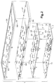
- Fig. 1 shows an isometric view of the input/output device of the preferred embodiment of the invention.
- Fig. 2 shows a rotated and exploded view of the input/output device of the preferred embodiment of the invention.
- Fig. 3 shows a fragmentary section view, taken along line A-A of Fig. 1, of the lamps and switches of the input/output device of the preferred embodiment of the invention.
- Fig. 4 shows an enlarged view, taken along line B-B of Fig. 3, of a lamp and a switch of the input/output device of the preferred embodiment of the invention.
- Fig. 5 shows how the input/output device of the preferred embodiment is manufactured.
- Fig. 1 shows an input/output device according to the preferred embodiment of the present invention.
- the term "input/output device” shall mean any keyboard, keypad, display, panel, mouse, or other device capable of communicating information to and from a user.
- the input/output device is shown as panel 1.
- Panel 1 is preferably a portion of electrocardiograph 100, although it could be a portion of other types of electronic equipment, such as a computer, audio equipment, video equipment, instrumentation, etc, and still fall within the spirit and scope of the invention.
- Panel 1 includes at least one switch 3 and at least one lamp 5.
- Fig. 2 is a rotated and exploded view of the input/output device according to the preferred embodiment of the invention.
- Panel 1 contains overlay 29, frame 27, membrane 13, and circuit board 7.
- Circuit board 7 contains light emitting portion 25 of lamp 5.
- light emitting portion 25 is a light emitting diode, although other light emitting devices, such as fluorescent or electro-luminescent devices, could be used and still fall within the spirit and scope of the invention.
- Circuit board 7 also contains tabs 15 and trace portions 23 of switch 3, and optionally contains other components, connectors, wires, traces, etc.
- Membrane 13 is formed over the upper surface of circuit board 7 and continuously extends over at least light emitting portion 25 and trace portions 23.
- Membrane 13 is preferably formed of a resilient, flexible, at least partially translucent material with electrically insulative properties, such as silicone rubber.
- Membrane 13 contains light pipe portion 35 of lamp 5, and actuation portion 33 of switch 3.
- Membrane 13 also contains electrically conductive portion 43 of switch 3, but this portion is hidden from view in Fig. 2 by actuation portion 33.
- electrically conductive portion 43 is not made of the same material as the rest of membrane 13, but instead is made of a conductive elastimer or other conductive material.
- the remainder of membrane 13 is translucent or transparent, although those skilled in the art will appreciate that only light pipe portion 35 needs to be translucent or transparent, so that light can be transmitted from light emitting portion 25 up to the surface of panel 1.
- Membrane 13 is secured to circuit board 7 by engagement of a plurality of posts 17 formed integrally with and depending from membrane 13 and interference fit into corresponding apertures 19 in circuit board 7.
- Membrane 13 serves to seal circuit board 7 and the components carried thereon against contamination and to insulate them against electrostatic discharge from an operator's fingers or other objects contacting panel 1, switch 3, or lamp 5.
- Circuit board 7 and membrane 13 are secured to frame 27 by engagement between tabs 15 in circuit board 7 and retaining snaps 58 in frame 27, thereby capturing membrane 13 in between.
- Light pipe portion 35 and actuation portion 33 of membrane 13 go through apertures 55 and 53, respectively, in frame 27.
- Overlay 29 is secured to frame 27 by engagement between tabs 66 in overlay 29 and slots 56 in frame 27.
- Light pipe portion 35 and actuation portion 33 of membrane 13 go through apertures 65 and 63, respectively, in overlay 29.
- overlay 29 contains textual information 69 describing the function of various switches and/or lights on panel 1.
- Overlay 29 is preferably localized for a particular country and language, and is easily affixable to frame 27.
- a first alternate embodiment has been contemplated where textual information is either not required or is written directly on frame 27 or on light pipe portion 35 or actuation portion 33 of membrane 13. In this embodiment, panel 1 does not contain overlay 29.
- a second alternate embodiment has been contemplated where textual information is either not required or is written directly on membrane 13. In this embodiment, panel 1 does not contain overlay 29 or frame 27. Overlay 29 can also be easily removed by the user for cleaning with conventional soap and water.
- Fig. 3 shows a fragmentary section view, taken along line A-A of Fig. 1, of the lamps and switches of the input/output device of the preferred embodiment of the invention
- Fig. 4 shows an enlarged view taken along line B-B of Fig. 3.
- Fig. 4 shows switch 3 in an open position, since electrically conductive portion 43 is not in contact with trace portions 23.
- actuation portion 33 of switch 3 is deflected downwardly by a user or other force, air pocket 21 is compressed, and electrically conductive portion 43 contacts trace portions 23. This contact between electrically conductive portion 43 and trace portions 23 completes the circuit between trace portions 23.
- Fig. 5 shows how the input/output device of the preferred embodiment is manufactured.
- Circuit board 7 is manufactured/populated in a conventional manner in step 210.
- Steps 220-240 manufacture membrane 13 in the following manner.
- Conductive elastimer used to make portions 43 of switch 3 is placed in nest areas in the membrane mold in step 220.
- An insulating elastimer, such as silicone rubber, is then placed in the membrane mold in step 230.
- the membrane mold is heated in step 240, the conductive elastimer chemically and mechanically bonds with the insulating elastimer.
- the insulating elastimer forms light pipe portion 35, actuation portion 33, posts 17, and the remainder of membrane 13.
- Membrane 13 is attached to circuit board 7 in step 250 by fitting posts 17 into apertures 19 (Fig. 2).
- Frame 27 is manufactured conventionally using resin transfer techniques in step 260.
- Frame 27 is attached to membrane 13 and circuit board 7 in step 270 by inserting tabs 15 in circuit board 7 into retaining snaps 58 in frame 27.
- Light pipe portion 35 and actuation portion 33 of membrane 13 are inserted through apertures 55 and 53, respectively, in frame 27.
- Overlay is manufactured conventionally using resin transfer techniques in step 280.
- Overlay 29 is secured to frame 27 in step 290 by engagement between tabs 66 in overlay 29 and slots 56 in frame 27.
- Light pipe portion 35 and actuation portion 33 of membrane 13 go through apertures 65 and 63, respectively, in overlay 29.
Landscapes
- Push-Button Switches (AREA)
- Casings For Electric Apparatus (AREA)
Applications Claiming Priority (2)
| Application Number | Priority Date | Filing Date | Title |
|---|---|---|---|
| US310185 | 1981-10-09 | ||
| US31018594A | 1994-09-21 | 1994-09-21 |
Publications (1)
| Publication Number | Publication Date |
|---|---|
| EP0703591A1 true EP0703591A1 (fr) | 1996-03-27 |
Family
ID=23201356
Family Applications (1)
| Application Number | Title | Priority Date | Filing Date |
|---|---|---|---|
| EP95305266A Withdrawn EP0703591A1 (fr) | 1994-09-21 | 1995-07-28 | Dispositif d'entrée/sortie avec une lampe et un interrupteur avec protection contre les décharges électrostatiques et la contamination |
Country Status (3)
| Country | Link |
|---|---|
| EP (1) | EP0703591A1 (fr) |
| JP (1) | JPH08204346A (fr) |
| CN (1) | CN1123454A (fr) |
Cited By (4)
| Publication number | Priority date | Publication date | Assignee | Title |
|---|---|---|---|---|
| WO1998039785A1 (fr) * | 1997-03-03 | 1998-09-11 | Telefonaktiebolaget Lm Ericsson | Protection contre les decharges electrostatiques dans un dispositif de telecommunication portable |
| WO2000077805A1 (fr) * | 1999-05-27 | 2000-12-21 | Storage Technology Corporation | Panneau d'interfaçage protege contre les decharges electrostatiques (esd) et methodes correspondantes |
| US8144036B2 (en) | 2007-02-08 | 2012-03-27 | Lear Corporation | Switch system |
| CN103915278A (zh) * | 2014-03-26 | 2014-07-09 | 海门市曼博莱电子发展有限公司 | 一种薄膜开关 |
Families Citing this family (1)
| Publication number | Priority date | Publication date | Assignee | Title |
|---|---|---|---|---|
| JP2005353412A (ja) * | 2004-06-10 | 2005-12-22 | Alps Electric Co Ltd | 板バネ付シート、及びこの板バネ付シートを使用したスイッチ装置 |
Citations (9)
| Publication number | Priority date | Publication date | Assignee | Title |
|---|---|---|---|---|
| GB1312740A (en) * | 1971-12-02 | 1973-04-04 | Standard Telephones Cables Ltd | Push buttons |
| GB2065373A (en) * | 1979-12-07 | 1981-06-24 | Shinetsu Polymer Co | Illuminated key-board switch unit |
| FR2517646A1 (fr) | 1981-12-07 | 1983-06-10 | Si Handling Systems | Piste pour vehicules sans conducteur |
| FR2517846A1 (fr) * | 1981-12-07 | 1983-06-10 | Thomson Csf Mat Tel | Dispositif de visualisation etanche, et clavier de commande comportant un tel dispositif |
| US4458123A (en) | 1982-09-03 | 1984-07-03 | Oak Industries, Inc. | Connector for attaching an electrical component to a membrane keyboard |
| US4636593A (en) * | 1985-03-13 | 1987-01-13 | Motorola Inc. | Light conducting, elastomeric membrane keypad |
| DE3541776A1 (de) | 1985-11-26 | 1987-05-27 | Siemens Ag | Optische anzeigevorrichtung fuer elektrische geraete |
| EP0358885A1 (fr) | 1988-09-15 | 1990-03-21 | Hagenuk Gmbh | Membrane de recouvrement pour plaquette de circuit |
| US5149923A (en) | 1991-03-15 | 1992-09-22 | Lucas Duralith Corporation | Backlit tactile keyboard with improved tactile and electrical characteristics |
-
1995
- 1995-07-28 EP EP95305266A patent/EP0703591A1/fr not_active Withdrawn
- 1995-09-18 CN CN 95115743 patent/CN1123454A/zh active Pending
- 1995-09-21 JP JP26792195A patent/JPH08204346A/ja active Pending
Patent Citations (9)
| Publication number | Priority date | Publication date | Assignee | Title |
|---|---|---|---|---|
| GB1312740A (en) * | 1971-12-02 | 1973-04-04 | Standard Telephones Cables Ltd | Push buttons |
| GB2065373A (en) * | 1979-12-07 | 1981-06-24 | Shinetsu Polymer Co | Illuminated key-board switch unit |
| FR2517646A1 (fr) | 1981-12-07 | 1983-06-10 | Si Handling Systems | Piste pour vehicules sans conducteur |
| FR2517846A1 (fr) * | 1981-12-07 | 1983-06-10 | Thomson Csf Mat Tel | Dispositif de visualisation etanche, et clavier de commande comportant un tel dispositif |
| US4458123A (en) | 1982-09-03 | 1984-07-03 | Oak Industries, Inc. | Connector for attaching an electrical component to a membrane keyboard |
| US4636593A (en) * | 1985-03-13 | 1987-01-13 | Motorola Inc. | Light conducting, elastomeric membrane keypad |
| DE3541776A1 (de) | 1985-11-26 | 1987-05-27 | Siemens Ag | Optische anzeigevorrichtung fuer elektrische geraete |
| EP0358885A1 (fr) | 1988-09-15 | 1990-03-21 | Hagenuk Gmbh | Membrane de recouvrement pour plaquette de circuit |
| US5149923A (en) | 1991-03-15 | 1992-09-22 | Lucas Duralith Corporation | Backlit tactile keyboard with improved tactile and electrical characteristics |
Cited By (8)
| Publication number | Priority date | Publication date | Assignee | Title |
|---|---|---|---|---|
| WO1998039785A1 (fr) * | 1997-03-03 | 1998-09-11 | Telefonaktiebolaget Lm Ericsson | Protection contre les decharges electrostatiques dans un dispositif de telecommunication portable |
| US6207912B1 (en) | 1997-03-03 | 2001-03-27 | Telefonaktiebolaget Lm Ericsson | Electrostatic discharge protection in a portable communication device |
| AU732251B2 (en) * | 1997-03-03 | 2001-04-12 | Telefonaktiebolaget Lm Ericsson (Publ) | Electrostatic discharge protection in a portable communication device |
| RU2204871C2 (ru) * | 1997-03-03 | 2003-05-20 | Телефонактиеболагет Лм Эрикссон | Защита от электростатического разряда в переносном устройстве связи |
| WO2000077805A1 (fr) * | 1999-05-27 | 2000-12-21 | Storage Technology Corporation | Panneau d'interfaçage protege contre les decharges electrostatiques (esd) et methodes correspondantes |
| US6331928B1 (en) | 1999-05-27 | 2001-12-18 | Storage Technology Corporation | ESD-protected interface panel and associated methods |
| US8144036B2 (en) | 2007-02-08 | 2012-03-27 | Lear Corporation | Switch system |
| CN103915278A (zh) * | 2014-03-26 | 2014-07-09 | 海门市曼博莱电子发展有限公司 | 一种薄膜开关 |
Also Published As
| Publication number | Publication date |
|---|---|
| CN1123454A (zh) | 1996-05-29 |
| JPH08204346A (ja) | 1996-08-09 |
Similar Documents
| Publication | Publication Date | Title |
|---|---|---|
| EP1039493B1 (fr) | Interrupteur en feuille combiné électroluminescent | |
| US7485824B2 (en) | Electrical switch component | |
| US5847336A (en) | Direct keypad backlighting | |
| CN100511530C (zh) | 用于便携式设备的具有按键支撑结构的键盘 | |
| US5770914A (en) | Illuminated piezoelectric switch | |
| US8168904B2 (en) | Illumination button switch assembly having lighting structure and electronic device | |
| US8258987B2 (en) | Icon illumination for capacitive touch switch | |
| US6670565B2 (en) | Illuminated button switch | |
| GB2276767A (en) | Selectively illuminated indicator | |
| US20070018965A1 (en) | Illuminated touch control interface | |
| US5442150A (en) | Piezo electric switch | |
| US6057517A (en) | Elastomeric keyboard incorporating a novel interconnect and back-lighting architecture | |
| US4796007A (en) | Micro-motion keyboard | |
| US6552289B2 (en) | Dome switch | |
| US20240345664A1 (en) | Through Hole Keyboard | |
| US6278069B1 (en) | Apparatus and method for supplying power to an electronic system | |
| EP0703591A1 (fr) | Dispositif d'entrée/sortie avec une lampe et un interrupteur avec protection contre les décharges électrostatiques et la contamination | |
| JP2022140759A (ja) | 表示構造 | |
| TW563144B (en) | Lighting unit and lighting apparatus using the same unit | |
| JP3208402B2 (ja) | 発光式スイッチ | |
| CN1192582C (zh) | 具有可换壳部的装置 | |
| TWI595523B (zh) | 發光鍵盤及鍵盤模組 | |
| US4417114A (en) | Connector for attaching an electrical component to a flat sheet | |
| JP3279809B2 (ja) | 電子機器の操作装置 | |
| JP2003306275A (ja) | エレベータ用押しボタンスイッチ |
Legal Events
| Date | Code | Title | Description |
|---|---|---|---|
| PUAI | Public reference made under article 153(3) epc to a published international application that has entered the european phase |
Free format text: ORIGINAL CODE: 0009012 |
|
| AK | Designated contracting states |
Kind code of ref document: A1 Designated state(s): DE FR GB IT |
|
| 17P | Request for examination filed |
Effective date: 19960607 |
|
| STAA | Information on the status of an ep patent application or granted ep patent |
Free format text: STATUS: THE APPLICATION HAS BEEN WITHDRAWN |
|
| 18W | Application withdrawn |
Withdrawal date: 19970626 |