EP0703613A2 - Schutz elektronischer Bauelemente in saurer und basischer Umgebung - Google Patents
Schutz elektronischer Bauelemente in saurer und basischer Umgebung Download PDFInfo
- Publication number
- EP0703613A2 EP0703613A2 EP95114227A EP95114227A EP0703613A2 EP 0703613 A2 EP0703613 A2 EP 0703613A2 EP 95114227 A EP95114227 A EP 95114227A EP 95114227 A EP95114227 A EP 95114227A EP 0703613 A2 EP0703613 A2 EP 0703613A2
- Authority
- EP
- European Patent Office
- Prior art keywords
- coating
- corrosive
- corrosive agent
- buffer
- acid
- Prior art date
- Legal status (The legal status is an assumption and is not a legal conclusion. Google has not performed a legal analysis and makes no representation as to the accuracy of the status listed.)
- Withdrawn
Links
Images
Classifications
-
- H—ELECTRICITY
- H10—SEMICONDUCTOR DEVICES; ELECTRIC SOLID-STATE DEVICES NOT OTHERWISE PROVIDED FOR
- H10W—GENERIC PACKAGES, INTERCONNECTIONS, CONNECTORS OR OTHER CONSTRUCTIONAL DETAILS OF DEVICES COVERED BY CLASS H10
- H10W74/00—Encapsulations, e.g. protective coatings
- H10W74/40—Encapsulations, e.g. protective coatings characterised by their materials
- H10W74/47—Encapsulations, e.g. protective coatings characterised by their materials comprising organic materials, e.g. plastics or resins
-
- H—ELECTRICITY
- H10—SEMICONDUCTOR DEVICES; ELECTRIC SOLID-STATE DEVICES NOT OTHERWISE PROVIDED FOR
- H10W—GENERIC PACKAGES, INTERCONNECTIONS, CONNECTORS OR OTHER CONSTRUCTIONAL DETAILS OF DEVICES COVERED BY CLASS H10
- H10W74/00—Encapsulations, e.g. protective coatings
- H10W74/10—Encapsulations, e.g. protective coatings characterised by their shape or disposition
- H10W74/111—Encapsulations, e.g. protective coatings characterised by their shape or disposition the semiconductor body being completely enclosed
- H10W74/121—Encapsulations, e.g. protective coatings characterised by their shape or disposition the semiconductor body being completely enclosed by multiple encapsulations, e.g. by a thin protective coating and a thick encapsulation
-
- H—ELECTRICITY
- H10—SEMICONDUCTOR DEVICES; ELECTRIC SOLID-STATE DEVICES NOT OTHERWISE PROVIDED FOR
- H10W—GENERIC PACKAGES, INTERCONNECTIONS, CONNECTORS OR OTHER CONSTRUCTIONAL DETAILS OF DEVICES COVERED BY CLASS H10
- H10W74/00—Encapsulations, e.g. protective coatings
- H10W74/40—Encapsulations, e.g. protective coatings characterised by their materials
- H10W74/47—Encapsulations, e.g. protective coatings characterised by their materials comprising organic materials, e.g. plastics or resins
- H10W74/473—Encapsulations, e.g. protective coatings characterised by their materials comprising organic materials, e.g. plastics or resins containing a filler
-
- H—ELECTRICITY
- H10—SEMICONDUCTOR DEVICES; ELECTRIC SOLID-STATE DEVICES NOT OTHERWISE PROVIDED FOR
- H10W—GENERIC PACKAGES, INTERCONNECTIONS, CONNECTORS OR OTHER CONSTRUCTIONAL DETAILS OF DEVICES COVERED BY CLASS H10
- H10W72/00—Interconnections or connectors in packages
- H10W72/50—Bond wires
- H10W72/551—Materials of bond wires
- H10W72/552—Materials of bond wires comprising metals or metalloids, e.g. silver
- H10W72/5522—Materials of bond wires comprising metals or metalloids, e.g. silver comprising gold [Au]
-
- H—ELECTRICITY
- H10—SEMICONDUCTOR DEVICES; ELECTRIC SOLID-STATE DEVICES NOT OTHERWISE PROVIDED FOR
- H10W—GENERIC PACKAGES, INTERCONNECTIONS, CONNECTORS OR OTHER CONSTRUCTIONAL DETAILS OF DEVICES COVERED BY CLASS H10
- H10W72/00—Interconnections or connectors in packages
- H10W72/851—Dispositions of multiple connectors or interconnections
- H10W72/874—On different surfaces
- H10W72/884—Die-attach connectors and bond wires
-
- H—ELECTRICITY
- H10—SEMICONDUCTOR DEVICES; ELECTRIC SOLID-STATE DEVICES NOT OTHERWISE PROVIDED FOR
- H10W—GENERIC PACKAGES, INTERCONNECTIONS, CONNECTORS OR OTHER CONSTRUCTIONAL DETAILS OF DEVICES COVERED BY CLASS H10
- H10W74/00—Encapsulations, e.g. protective coatings
-
- H—ELECTRICITY
- H10—SEMICONDUCTOR DEVICES; ELECTRIC SOLID-STATE DEVICES NOT OTHERWISE PROVIDED FOR
- H10W—GENERIC PACKAGES, INTERCONNECTIONS, CONNECTORS OR OTHER CONSTRUCTIONAL DETAILS OF DEVICES COVERED BY CLASS H10
- H10W90/00—Package configurations
- H10W90/701—Package configurations characterised by the relative positions of pads or connectors relative to package parts
- H10W90/731—Package configurations characterised by the relative positions of pads or connectors relative to package parts of die-attach connectors
- H10W90/734—Package configurations characterised by the relative positions of pads or connectors relative to package parts of die-attach connectors between a chip and a stacked insulating package substrate, interposer or RDL
-
- H—ELECTRICITY
- H10—SEMICONDUCTOR DEVICES; ELECTRIC SOLID-STATE DEVICES NOT OTHERWISE PROVIDED FOR
- H10W—GENERIC PACKAGES, INTERCONNECTIONS, CONNECTORS OR OTHER CONSTRUCTIONAL DETAILS OF DEVICES COVERED BY CLASS H10
- H10W90/00—Package configurations
- H10W90/701—Package configurations characterised by the relative positions of pads or connectors relative to package parts
- H10W90/751—Package configurations characterised by the relative positions of pads or connectors relative to package parts of bond wires
- H10W90/754—Package configurations characterised by the relative positions of pads or connectors relative to package parts of bond wires between a chip and a stacked insulating package substrate, interposer or RDL
-
- Y—GENERAL TAGGING OF NEW TECHNOLOGICAL DEVELOPMENTS; GENERAL TAGGING OF CROSS-SECTIONAL TECHNOLOGIES SPANNING OVER SEVERAL SECTIONS OF THE IPC; TECHNICAL SUBJECTS COVERED BY FORMER USPC CROSS-REFERENCE ART COLLECTIONS [XRACs] AND DIGESTS
- Y10—TECHNICAL SUBJECTS COVERED BY FORMER USPC
- Y10T—TECHNICAL SUBJECTS COVERED BY FORMER US CLASSIFICATION
- Y10T428/00—Stock material or miscellaneous articles
- Y10T428/23—Sheet including cover or casing
- Y10T428/239—Complete cover or casing
Definitions
- This invention relates to the protection of electronic components in acidic and basic environments. More particularly, our invention describes a method of imparting to conventional organic polymeric encapsulants greater protective qualities to sensitive electronic devices in the presence of a highly acidic or basic environment. Even more specifically our invention relates to elastomeric silicones affording heightened acid and base protection to encapsulated materials.
- encapsulation The purpose of encapsulation is to protect electronic IC devices from moisture, ionic contaminants such as mobile sodium, potassium, and chloride ions, uv and alpha particle radiation, and other hostile operating environments including corrosive agents such as acids, bases, and oxidizing agents.
- encapsulation enhances the mechanical and physical properties of fragile IC devices and improves manufacturing yields and reliability.
- the encapsulant must be an ultrapure material with an excellent barrier to moisture and contaminant mobile ions with superior electrical, physical, and mechanical properties, and which is easy to apply and to repair in production. See Encyclopedia of Polymer Science and Engineering, V 5, pp 638-641, J. Wiley & Sons (1989).
- encapsulants both inorganic and organic polymers
- encapsulants are available having a broad spectrum of properties, and generally the choice of encapsulants is made depending upon necessary properties which are a consequence of the working environment.
- a need for outstanding solvent resistance may dictate one type of encapsulant
- a need for high temperature stability may require a quite different type of encapsulant.
- the nature and properties of available encapsulants are sufficiently well known that the worker in this field can make an intelligent choice which will be well suited to the task at hand.
- This application is directed to one sort of such extreme; our invention is a solution to the unusual demands of a particularly unfriendly environment.
- the piezoresistive transducer in question is a monolithic silicon chip.
- the output voltage varies with pressure via a resistive element, acting as a strain gauge, implanted on a thin silicon diaphragm.
- the resulting die is aluminum metallized, with bond pads for, e.g., gold wire bonds to connect the chip to the lead frame and the die is mounted on a room temperature vulcanizing (RTV) elastomer, exemplified by a silicone or fluorosilicone, to the package base.
- RTV room temperature vulcanizing
- the die, including the wire bond pads is encapsulated in a protective polymer coating.
- the encapsulant Since the function of the die is to measure pressure, the encapsulant must not be a rigid, non-deformable polymer but instead must transmit external pressure changes to the die.
- the encapsulant is an elastomer, which can be described variously as a rubbery, gummy, or gel-like material, and silicones, including fluorosilicones, are the elastomers of choice, in part because of their excellent resistance to water and hydrocarbon vapors which are a normal incident of the environment in which the manifold absolute pressure sensor is placed.
- silicones including fluorosilicones
- the solution to the problem must be directed either to eliminating or reducing permeation of acids through the encapsulant, or to neutralize acids within the encapsulating polymer.
- Our solution to the problem is to disperse a solid buffer within the elastomer, which certainly serves to neutralize acids but, depending upon how the elastomer is used, also may prevent permeation of the encapsulating elastomer by offending acids.
- buffer in its most extended chemical sense, i.e., a substance which resists a change in hydrogen ion concentration upon addition of acids or alkali, or a substance which resists a change in oxidation potential.
- the former is more generally intended within this application; this class is referred to as “acid-base buffers.”
- buffer shall mean an “acid-base buffer.”
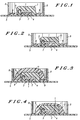
- Figure 1 is a side view of an encapsulated device according to the prior art.
- Figures 2 - 4 are embodiments of an encapsulated device protected against corrosive agents according to our invention.
- our invention is a method of either inhibiting permeation of agents corrosive to the material of construction of integrated circuits through the polymeric material encapsulating the integrated circuit, or a method of neutralizing a corrosive agent within the encapsulant, by dispersing a buffer within the encapsulating polymer itself or by providing the encapsulant with a protective polymeric coating containing the buffer.
- the corrosive agent is an acid, base, or oxidant.
- the corrosive agent is an acid.
- the corrosive agent is an acidic material typically found in the manifold intake of internal combustion engines.
- the polymeric encapsulant is an elastomer.
- the elastomer is a silicone.
- the buffer consists of solid particles of, for example alumina or magnesia hydrates.
- a different set of embodiments directed to the inhibition of permeation of corrosive agents into the encapsulating layer, constitutes a second, protective polymer layer over the encapsulating polymer, where the protective layer contains a buffer. In this way the corrosive agent is prevented from reaching the encapsulating polymer.
- both the protective and encapsulating polymers are elastomers.
- both elastomeric polymers are silicones.
- the buffer is a dispersion of solid particles of alumina or magnesia hydrates.
- sicones is a generic term applied to silicon-based polymers generally, and includes materials variously described as siloxanes, polysiloxanes, polyfluorosiloxanes, inter alia , within the class.
- polymeric encapsulants The purpose of polymeric encapsulants is to protect the underlying integrated circuit from corrosive agents and other agents which interfere with normal functioning of the integrated circuit.
- corrosive agents For example, water and alkali metal cations are well known interfering agents, although they are not normally considered as corrosive agents.
- acids, bases, and oxidizing agents are well known interfering agents, although they are not normally considered as corrosive agents.
- acids acids, bases, and oxidizing agents, but most importantly acids.
- acids which can act as corrosive agents the following may be mentioned; nitric acid (and the oxides of nitrogen generally), sulfuric acid (and the oxides of sulfur generally), hydrochloric acid, phosphoric acids, and organic acids to a lesser extent.
- Nitric and sulfuric acids are of principal interest here for they, along with the other acidic oxides of nitrogen and sulfur, are most likely to be found in the intake manifold of internal combustion engines.
- bases which may serve as corrosive agents may be mentioned the alkali metal hydroxides generally and ammonia.
- oxidizing agents which can serve as corrosive agents may be mentioned nitrogen oxides generally, especially the higher nitrogen oxides such as NO2 and N2O3.
- a buffer is a substance which resists a change in hydrogen ion concentration upon the addition of acid or alkali, or which resists a change in oxidation potential, but for use in our invention the buffer must be material which does not interfere with the formation of the polymer or significantly change the properties of the polymeric material when incorporated therein. Because aluminum oxide hydrates are amphoteric, i.e., can act either as an acid or base under appropriate conditions, we have found that aluminum oxide hydrates are outstanding acid-base buffers in the practice of our invention.
- acid buffers which may be used in our invention include the hydrates of magnesium and calcium oxides and their hydrates, borates of alkali metals, acetates (and carboxylates generally) of alkali metals, potassium dihydrogen phosphate-disodium phosphate (KH2PO4-Na2HPO4), potassium acid phosphate-sodium hydroxide, borax, boric acid-sodium hydroxide, calcium carbonate-calcium hydrogen carbonate, and so forth.
- Basic buffers include such materials as primary potassium citrate, secondary sodium citrate, and tris-(hydroxymethyl)aminomethane and its hydrochloride, and sodium carbonate-sodium hydroxide. See generally D. D. Perrin and B.
- Buffers for pH and Metal Ion Control (1979). Particle sizes in the range of 0.02-50 microns in diameter may be used in the practice of our invention, although it is recommended that particles be in the 0.5-10 micron diameter range. Buffers may be added in an amount, relative to the elastomer or other polymeric encapsulant, as low as 1 weight percent up to as high as 25 weight percent, but additions of 10-20 weight percent are preferred.
- Figure 1 represents the prior art.
- the electronic device 1 which in the case of immediate interest is a piezoresistive transducer, is mounted on a cushion 2, or a thick disk, of a suitable elastomer, generally a room temperature vulcanized silicone.
- the device is placed on the top surface 3 of the disk whose bottom surface 4 is attached to circuit board 5 .
- Wire connectors, here represented by the single connector 6 lead from the device via bond pads (not shown) to the circuit board.
- the entire device, including wire connectors, is encapsulated in a suitable protective polymeric coating 7 .
- the protective polymeric coating must itself be readily deformable and compliant so as to accurately transmit pressure changes to the encapsulated device. Consequently, the encapsulating polymer in this case is elastomeric, and silicones constitute the outstanding example of elastomeric encapsulants used in devices of this type.
- the entire device is housed in a semi-enclosed structure, i.e., one enclosed on three sides but open on the fourth so as to be in communication with the pressure source.
- a semi-enclosed structure i.e., one enclosed on three sides but open on the fourth so as to be in communication with the pressure source.
- this may be accomplished by having the circuit board as one of the closed sides and having the sides of a cylinder surrounding the device and itself connected to the circuit board form the other sides 8 completing the enclosure.
- a sealing gel 9 often is placed as a continuous, pressure-tight film between the encapsulated device and the cylinder sides 8, thereby effectively sealing the housing at places prone to leaks.
- One mode of practicing our invention is to incorporate the buffer directly into the encapsulant, as depicted in Figure 2.
- This variant is unquestionably the simplest to effect, since it requires minimal changes in the overall manufacturing process.
- the sole difference between this variant and that depicted in Figure 1 is the presence of a solid buffer dispersed (more-or-less uniformly) within the protective polymeric coating, i.e., the encapsulating polymer 10 is different from 7 in having present a dispersion of solid buffer particles.
- the buffer acts to neutralize the corrosive agent permeating the encapsulating polymer and prevents corrosive attack on the underlying device.
- the corrosive agent is an acid, which represents perhaps the chief problem
- the solid buffer serves to neutralize the acid.
- the outer, buffered protective polymeric layer effectively isolates both the encapsulant and the seal gel from the environment.
- the outer, buffered polymeric protective layer prevents or inhibits permeation of corrosive materials into the encapsulating polymer by neutralizing the offending corrosive agent.
- the encapsulant "sees" a corrosive-free environment; this variant may be viewed as effectively changing the environment in which the encapsulant is placed.
- Figure 4 depicts a mode where the buffer is incorporated into an elastomer which provides both an outer, protective layer to the encapsulant itself and which also acts as the seal gel.
- the outer buffered protective polymer layer 12 prevents or inhibits permeation of corrosive materials into the encapsulating polymer by neutralizing the offending corrosive agent while acting as a sealing agent.
- the environment presented to the encapsulant is free of corrosive agents.
- This variant also may be viewed as effectively changing the environment in which the encapsulant is placed. Note that in this variant, as in the prior one, the outer protective polymeric layer also must be an elastomer which readily transmits pressure changes, and in general must function in this regard identically to the encapsulant.
- the buffer must be an acid-base buffer tending to neutralize the basic medium.
- the buffer must be capable of reducing the oxidation potential so as to inhibit corrosion of the IC.
- a silicone adhesive acting as a cushion for the piezoresistive transducer die is dispensed onto an alumina substrate, and the die is placed on the top surface of the adhesive. After the silicone is cured, the die is wire bonded to the substrate.
- a thixotropic fluorinated siloxane (polyfluorosiloxane) is then dispensed on top of the die and wire bonds and cured to serve as the encapsulant; see figure 1.
- a second fluorosiloxane, serving as the sealing gel is then dispensed into the can and cured.
- a standardized, accelerated test was devised to determine failure time for these devices in the presence of nitric acid. Under standard test conditions devices prepared as above failed within 125 hours.
- Method of the Invention Preparation of the device begun as described above with deposit of a silicone adhesive as a cushion for the piezoresistive transducer die, placement of the die on the adhesive, and curing.
- a buffered gel was prepared by adding under vacuum to the fluorinated siloxane of the prior art method 7.5 weight percent each (based on final product gel) magnesium hydroxide and aluminum hydroxide. Additional Pt catalyst was added, to compensate for poisoning caused by the buffer, in an amount from 0.001-0.2 weight percent, but generally in the range of 0.01-0.1 weight percent. There was also added an inhibitor to give the polymer a useful pot life, and about 3 weight percent silica was added to give the siloxane thixotropic properties.
- the mixture was stirred under vacuum until a homogeneous paste was formed, thereafter dispensed on top of the die and wire bonds as described above, and then cured.
- a sealing gel was subsequently dispensed into the can as described above.
- the buffered gel configured devices had a lifetime of 400-500 hours. Thus, lifetimes could be extended by 3- to 4-fold by incorporation of a suitable buffer in the encapsulating polymer.
Landscapes
- Structures Or Materials For Encapsulating Or Coating Semiconductor Devices Or Solid State Devices (AREA)
Applications Claiming Priority (2)
| Application Number | Priority Date | Filing Date | Title |
|---|---|---|---|
| US31225294A | 1994-09-26 | 1994-09-26 | |
| US312252 | 1994-09-26 |
Publications (2)
| Publication Number | Publication Date |
|---|---|
| EP0703613A2 true EP0703613A2 (de) | 1996-03-27 |
| EP0703613A3 EP0703613A3 (de) | 1996-06-05 |
Family
ID=23210582
Family Applications (1)
| Application Number | Title | Priority Date | Filing Date |
|---|---|---|---|
| EP95114227A Withdrawn EP0703613A3 (de) | 1994-09-26 | 1995-09-11 | Schutz elektronischer Bauelemente in saurer und basischer Umgebung |
Country Status (2)
| Country | Link |
|---|---|
| US (2) | US5686162A (de) |
| EP (1) | EP0703613A3 (de) |
Cited By (3)
| Publication number | Priority date | Publication date | Assignee | Title |
|---|---|---|---|---|
| DE19804748B4 (de) * | 1997-03-25 | 2008-06-05 | Freescale Semiconductor, Inc., Austin | Anordnung und Verfahren der Isolierung gegen mechanische Spannung bei der Befestigung von Halbleiterchips |
| DE102015204499A1 (de) | 2015-03-12 | 2016-09-15 | Robert Bosch Gmbh | Drucksensor zur Erfassung eines Drucks eines fluiden Mediums und Verfahren zum Herstellen desselben |
| DE102015206875A1 (de) | 2015-04-16 | 2016-10-20 | Robert Bosch Gmbh | Klebematerial zur mediengeschützten elektrisch leitenden Verbindung mindestens eines Leitungsträgers mit mindestens einem elektronischen Bauteil |
Families Citing this family (32)
| Publication number | Priority date | Publication date | Assignee | Title |
|---|---|---|---|---|
| US6097099A (en) * | 1995-10-20 | 2000-08-01 | Texas Instruments Incorporated | Electro-thermal nested die-attach design |
| US5996219A (en) * | 1997-01-31 | 1999-12-07 | The Board Of Trustees Of The Leland Stanford Junior University | Method for embedding electric or optical components in high-temperature metals |
| JPH1120729A (ja) * | 1997-07-02 | 1999-01-26 | Toyota Autom Loom Works Ltd | 車両におけるセンサの取付構造 |
| US6306688B1 (en) * | 1999-04-28 | 2001-10-23 | Teravicta Technologies, Inc. | Method of reworkably removing a fluorinated polymer encapsulant |
| US6413620B1 (en) * | 1999-06-30 | 2002-07-02 | Kyocera Corporation | Ceramic wiring substrate and method of producing the same |
| US6303860B1 (en) * | 1999-11-30 | 2001-10-16 | Bombardier Motor Corporation Of America | Bladder insert for encapsulant displacement |
| US6338976B1 (en) | 2000-01-21 | 2002-01-15 | Taiwan Semiconductor Manufacturing Company, Ltd. | Method for forming optoelectronic microelectronic fabrication with attenuated bond pad corrosion |
| DE10038508A1 (de) * | 2000-08-08 | 2002-02-21 | Bosch Gmbh Robert | Elektrische Baugruppe und Verfahren zur Herstellung der elektrischen Baugruppe |
| US20030059078A1 (en) * | 2001-06-21 | 2003-03-27 | Downs Edward F. | Directional sensors for head-mounted contact microphones |
| JP2003133484A (ja) * | 2001-10-30 | 2003-05-09 | Tokai Rika Co Ltd | 半導体装置及びその製造方法 |
| JP2003139593A (ja) * | 2001-11-07 | 2003-05-14 | Hitachi Ltd | 車載電子機器および熱式流量計 |
| US7177143B1 (en) | 2002-08-05 | 2007-02-13 | Communication Associates, Inc. | Molded electronic components |
| US20050001316A1 (en) * | 2003-07-01 | 2005-01-06 | Motorola, Inc. | Corrosion-resistant bond pad and integrated device |
| US7078796B2 (en) * | 2003-07-01 | 2006-07-18 | Freescale Semiconductor, Inc. | Corrosion-resistant copper bond pad and integrated device |
| JP2005033390A (ja) * | 2003-07-10 | 2005-02-03 | Citizen Watch Co Ltd | 圧電デバイスとその製造方法 |
| JP4818654B2 (ja) * | 2005-07-25 | 2011-11-16 | ソニーケミカル&インフォメーションデバイス株式会社 | 発光素子の封止方法 |
| US20070052047A1 (en) * | 2005-09-01 | 2007-03-08 | Costas Hadjiloucas | Metal contact systems for semiconductor-based pressure sensors exposed to harsh chemical and thermal environments |
| EP1938068A1 (de) * | 2005-09-16 | 2008-07-02 | STMicroelectronics S.r.l. | Drucksensor mit hohem vollausschlagswert mit kapselung dafür |
| US20080115772A1 (en) * | 2006-11-21 | 2008-05-22 | Ti Group Automotive Systems, L.L.C. | Fluid encapsulant for protecting electronics |
| DE102007032058A1 (de) * | 2007-07-10 | 2009-01-22 | Continental Automotive Gmbh | Sensor mit einer Messstelle, die von einem Passivierungsmittel bedeckt ist |
| US8116102B2 (en) * | 2007-12-26 | 2012-02-14 | Infineon Technologies Ag | Integrated circuit device and method of producing |
| US20090206431A1 (en) * | 2008-02-20 | 2009-08-20 | Micron Technology, Inc. | Imager wafer level module and method of fabrication and use |
| DE102011013912A1 (de) * | 2011-03-15 | 2012-09-20 | Volkswagen Aktiengesellschaft | Drucksensor |
| US9508622B2 (en) * | 2011-04-28 | 2016-11-29 | Freescale Semiconductor, Inc. | Method for protecting copper wire bonds on aluminum pads of a semiconductor device from corrosion |
| US20140191841A1 (en) * | 2013-01-04 | 2014-07-10 | International Business Machines Corporation | Conformal coating to scavenge elemental sulfur |
| KR20150125946A (ko) * | 2013-02-06 | 2015-11-10 | 더 보오드 오브 트러스티스 오브 더 유니버시티 오브 일리노이즈 | 인장성의 전자장치에 대한 자기 유사형 및 프랙탈 설계 |
| US9613911B2 (en) | 2013-02-06 | 2017-04-04 | The Board Of Trustees Of The University Of Illinois | Self-similar and fractal design for stretchable electronics |
| US10497633B2 (en) | 2013-02-06 | 2019-12-03 | The Board Of Trustees Of The University Of Illinois | Stretchable electronic systems with fluid containment |
| US10840536B2 (en) | 2013-02-06 | 2020-11-17 | The Board Of Trustees Of The University Of Illinois | Stretchable electronic systems with containment chambers |
| US9412709B2 (en) * | 2013-05-21 | 2016-08-09 | Freescale Semiconductor, Inc. | Semiconductor structure with sacrificial anode and passivation layer and method for forming |
| DE102016101694A1 (de) * | 2016-02-01 | 2017-08-03 | Infineon Technologies Ag | Korrosionsgeschütztes Elektronikmodul und Verfahren zu dessen Herstellung |
| DE102020208024A1 (de) * | 2020-06-29 | 2021-04-15 | Robert Bosch Gesellschaft mit beschränkter Haftung | Wasserdichte Drucksensoren mit einer bioziden Oberfläche sowie ein Herstellungsverfahren |
Family Cites Families (11)
| Publication number | Priority date | Publication date | Assignee | Title |
|---|---|---|---|---|
| US4529755A (en) * | 1982-10-23 | 1985-07-16 | Denki Kagaku Kogyo Kabushiki Kaisha | Epoxy resin composition for encapsulating semiconductor |
| JPS5998123A (ja) * | 1982-11-26 | 1984-06-06 | Sanyurejin Kk | 難燃性エポキシ樹脂組成物 |
| JP2757938B2 (ja) * | 1987-09-14 | 1998-05-25 | 日東電工株式会社 | 半導体装置 |
| US5104604A (en) * | 1989-10-05 | 1992-04-14 | Dexter Electronic Materials Div. Of Dexter Corp. | Flame retardant epoxy molding compound, method and encapsulated device method of encapsulating a semiconductor device with a flame retardant epoxy molding compound |
| JP2523204B2 (ja) * | 1990-03-19 | 1996-08-07 | 日本ペイント株式会社 | プレコ―ト金属材料用被覆組成物 |
| US5258650A (en) * | 1991-08-26 | 1993-11-02 | Motorola, Inc. | Semiconductor device having encapsulation comprising of a thixotropic fluorosiloxane material |
| US5165956A (en) * | 1991-09-27 | 1992-11-24 | At&T Bell Laboratories | Method of encapsulating an electronic device with a silicone encapsulant |
| US5252694A (en) * | 1992-01-22 | 1993-10-12 | Minnesota Mining And Manufacturing Company | Energy-polymerization adhesive, coating, film and process for making the same |
| US5346743A (en) * | 1992-03-13 | 1994-09-13 | Kabushiki Kaisha Toshiba | Resin encapsulation type semiconductor device |
| JPH065740A (ja) * | 1992-06-19 | 1994-01-14 | Mitsubishi Electric Corp | 半導体集積回路パッケージ装置 |
| JPH06220167A (ja) * | 1993-01-28 | 1994-08-09 | Toshiba Chem Corp | エポキシ樹脂組成物および半導体封止装置 |
-
1995
- 1995-09-11 EP EP95114227A patent/EP0703613A3/de not_active Withdrawn
-
1996
- 1996-01-31 US US08/594,385 patent/US5686162A/en not_active Expired - Lifetime
-
1997
- 1997-06-20 US US08/879,880 patent/US6030684A/en not_active Expired - Lifetime
Cited By (3)
| Publication number | Priority date | Publication date | Assignee | Title |
|---|---|---|---|---|
| DE19804748B4 (de) * | 1997-03-25 | 2008-06-05 | Freescale Semiconductor, Inc., Austin | Anordnung und Verfahren der Isolierung gegen mechanische Spannung bei der Befestigung von Halbleiterchips |
| DE102015204499A1 (de) | 2015-03-12 | 2016-09-15 | Robert Bosch Gmbh | Drucksensor zur Erfassung eines Drucks eines fluiden Mediums und Verfahren zum Herstellen desselben |
| DE102015206875A1 (de) | 2015-04-16 | 2016-10-20 | Robert Bosch Gmbh | Klebematerial zur mediengeschützten elektrisch leitenden Verbindung mindestens eines Leitungsträgers mit mindestens einem elektronischen Bauteil |
Also Published As
| Publication number | Publication date |
|---|---|
| US5686162A (en) | 1997-11-11 |
| US6030684A (en) | 2000-02-29 |
| EP0703613A3 (de) | 1996-06-05 |
Similar Documents
| Publication | Publication Date | Title |
|---|---|---|
| US6030684A (en) | Protecting electronic components in acidic and basic environment | |
| US6512255B2 (en) | Semiconductor pressure sensor device having sensor chip covered with protective member | |
| EP0736757B1 (de) | Korrosionsbeständiger Druckwandler durch anorganischen Überzug im Hohlraum | |
| CN1113226C (zh) | 带有气密封接的应力隔绝座以保护传感器芯的压力传感器 | |
| CN1914494A (zh) | 隔离的压力传感器 | |
| US6425294B1 (en) | Pressure sensor unit | |
| CN106017750A (zh) | 半导体应变仪 | |
| US7963154B2 (en) | Sensor unit for the measurment of a variable in a medium | |
| KR102484047B1 (ko) | Mems 감지 요소 및 와이어 접합부를 위한 인캡슐레이션 | |
| US7216545B2 (en) | Acid-resistant pressure sensor | |
| US6020648A (en) | Die structure using microspheres as a stress buffer for integrated circuit prototypes | |
| US20050284216A1 (en) | Sensor equipment having sensing portion and method for manufacturing the same | |
| Suhl | Thermally induced IC package cracking | |
| CN114551371A (zh) | 模块型半导体装置及模块型半导体装置的制造方法 | |
| US20050034526A1 (en) | Semiconductor sensor and method of plating semiconductor devices | |
| US6584853B2 (en) | Corrosion-proof pressure transducer | |
| JP2572120B2 (ja) | ポリマー/乾燥剤複合被覆 | |
| US6809423B1 (en) | Electronic module | |
| US20250157998A1 (en) | Micromechanical component and corresponding production method | |
| WO2020058512A1 (en) | Sensor apparatus | |
| Kubacki | Low temperature plasma deposition of silicon nitride to produce ultra-reliable, high performance, low cost sealed chip-on-board (SCOB) assemblies | |
| TWI779419B (zh) | 可降低半導體晶粒上應力之積體電路封裝 | |
| JP2633285B2 (ja) | 車載用混成集積回路装置 | |
| Suhir | Application of an Epoxy Cap in a Flip-Chip Package Design | |
| JP3384259B2 (ja) | 樹脂封止半導体装置 |
Legal Events
| Date | Code | Title | Description |
|---|---|---|---|
| PUAI | Public reference made under article 153(3) epc to a published international application that has entered the european phase |
Free format text: ORIGINAL CODE: 0009012 |
|
| AK | Designated contracting states |
Kind code of ref document: A2 Designated state(s): DE FR GB IT |
|
| PUAL | Search report despatched |
Free format text: ORIGINAL CODE: 0009013 |
|
| AK | Designated contracting states |
Kind code of ref document: A3 Designated state(s): DE FR GB IT |
|
| 17P | Request for examination filed |
Effective date: 19961205 |
|
| 17Q | First examination report despatched |
Effective date: 19971031 |
|
| STAA | Information on the status of an ep patent application or granted ep patent |
Free format text: STATUS: THE APPLICATION IS DEEMED TO BE WITHDRAWN |
|
| 18D | Application deemed to be withdrawn |
Effective date: 19991103 |