EP0703624A1 - Elément programmable dans les dispositifs à couches-barrière métalliques et procédé - Google Patents
Elément programmable dans les dispositifs à couches-barrière métalliques et procédé Download PDFInfo
- Publication number
- EP0703624A1 EP0703624A1 EP95401944A EP95401944A EP0703624A1 EP 0703624 A1 EP0703624 A1 EP 0703624A1 EP 95401944 A EP95401944 A EP 95401944A EP 95401944 A EP95401944 A EP 95401944A EP 0703624 A1 EP0703624 A1 EP 0703624A1
- Authority
- EP
- European Patent Office
- Prior art keywords
- metal
- layer
- aperture
- contact region
- semiconductor material
- Prior art date
- Legal status (The legal status is an assumption and is not a legal conclusion. Google has not performed a legal analysis and makes no representation as to the accuracy of the status listed.)
- Granted
Links
Images


Classifications
-
- H—ELECTRICITY
- H10—SEMICONDUCTOR DEVICES; ELECTRIC SOLID-STATE DEVICES NOT OTHERWISE PROVIDED FOR
- H10W—GENERIC PACKAGES, INTERCONNECTIONS, CONNECTORS OR OTHER CONSTRUCTIONAL DETAILS OF DEVICES COVERED BY CLASS H10
- H10W20/00—Interconnections in chips, wafers or substrates
- H10W20/40—Interconnections external to wafers or substrates, e.g. back-end-of-line [BEOL] metallisations or vias connecting to gate electrodes
- H10W20/49—Adaptable interconnections, e.g. fuses or antifuses
- H10W20/491—Antifuses, i.e. interconnections changeable from non-conductive to conductive
-
- H—ELECTRICITY
- H10—SEMICONDUCTOR DEVICES; ELECTRIC SOLID-STATE DEVICES NOT OTHERWISE PROVIDED FOR
- H10B—ELECTRONIC MEMORY DEVICES
- H10B20/00—Read-only memory [ROM] devices
- H10B20/20—Programmable ROM [PROM] devices comprising field-effect components
-
- Y—GENERAL TAGGING OF NEW TECHNOLOGICAL DEVELOPMENTS; GENERAL TAGGING OF CROSS-SECTIONAL TECHNOLOGIES SPANNING OVER SEVERAL SECTIONS OF THE IPC; TECHNICAL SUBJECTS COVERED BY FORMER USPC CROSS-REFERENCE ART COLLECTIONS [XRACs] AND DIGESTS
- Y10—TECHNICAL SUBJECTS COVERED BY FORMER USPC
- Y10S—TECHNICAL SUBJECTS COVERED BY FORMER USPC CROSS-REFERENCE ART COLLECTIONS [XRACs] AND DIGESTS
- Y10S257/00—Active solid-state devices, e.g. transistors, solid-state diodes
- Y10S257/926—Elongated lead extending axially through another elongated lead
Definitions
- This invention relates to metallization systems, and, in particular, to a metallization system for an integrated circuit having a barrier metal.
- Conductive metal films provide interconnections between contacts of devices in an integrated circuit and between the circuit and the outside world.
- a typical integrated circuit there is at least one layer of metal and often two or more layers of metal. While a number of metals are suitable for use in integrated circuits, aluminum is the metal most widely used for contacting devices and for interconnections of devices to the outside world.
- a first level of metal such as aluminum, provides ohmic contacts to surface contact regions of semiconductor devices. The ohmic contacts are separated from each other by one or more insulating regions.
- a second level of metal, also aluminum provides an interconnection between one or more first level metal contacts and the outside world.
- barrier metal layer between the silicon and the deposited aluminum.
- a typical barrier layer metal is titanium tungsten (Tiw). TiW acts as an adhesive layer and adheres to both silicon and aluminum. In addition, it has the property of preventing the migration or diffusion of aluminum into silicon.
- TiW titanium tungsten
- Such barrier metal layers are widely used in integrated circuits.
- Other barrier metals include, but are not limited to, TiN,& Ti.
- Certain integrated circuits also take advantage of the metal migration properties of aluminum deposited on silicon.
- Such devices are typically programmable devices and are typically diodes with Zener diodes being the preferred choice.
- the Zener diode under normal biasing conditions, is back biased and appears to be an open circuit.
- the Zener is subjected to high currents and high voltages, resulting in Joule heating, which cause one of its aluminum contacts to a Zener surface region to migrate through the junction of the Zener diode and effectively short out the diode.
- a Zener diode in its initial state and back biased will appear as an open circuit.
- a Zener diode programmed and shorted out by metal migration will appear as a short circuit or at least a very low resistance path as compared to a back biased Zener diode.
- Zener diodes lose their programmability since the barrier layer metal prevents the metal migration of aluminum into silicon and thereby prevents the programming of Zener type programmable devices.
- Programmable Zener diodes are often used in application specific integrated circuits (ASIC). Such circuits may be individually designed for a particular application. Alternatively, ASICs are often constructed from a number of so-called cells. Each cell represents a design of one circuit that is compatible in operation and manufacture with other circuits or cells. Together the cells form a library of modular circuit designs available for creating an ASIC. In ASICs, it is often desirable to combine predetermined integrated circuit cells with individually programmable cells where such programmable cells are programmable by the user or programmable at the end of the manufacturing process. In the manufacture of such ASICs, barrier metals are now widely used in order to prevent aluminum from penetrating into the surface of the silicon. However, the presence of the barrier metal interferes with those ASICs that rely upon programmable Zener diodes.
- An object of the invention is to provide a programmable device in an integrated circuit with a barrier metal system for programming a Zener diode.
- the invention provides an integrated circuit having one or more programmable devices such as programmable Zener diodes.
- the integrated circuit of the invention is formed on a substrate of semiconductor material.
- the substrate has a surface and in that surface a programmable device is formed, preferably a programmable Zener diode.
- the programmable device has first and second surface contact regions for receiving first and second level metal contacts.
- a first thin oxide layer is grown or deposited on the substrate.
- a layer of polysilicon is deposited on the first thin oxide to form gates and define the Zener diffusion.
- a field oxide separates adjacent devices.
- a second oxide layer is deposited over the surface of the polysilicon material.
- the second oxide layer is etched or patterned to expose over the polysilicon and the first and second surface contact regions in the semiconductor material for the purpose of defining regions to be silicided and to provide sidewall oxide spaces.
- a third oxide layer is deposited and patterned to establish apertures for a first level metal. The apertures are filled with a first level of metal.
- the first level of metal includes a barrier metal layer. A layer of metal, e.g., aluminum, is deposited on the barrier layer. In the preferred embodiment, the barrier metal layer is typically TiW.
- the first level of metal is patterned and etched to remove it from selective second contact surface regions of the semiconductor that form one of the terminals of the Zener diode.
- the first level metal is masked and the metal is removed so that the metal deposited in the second aperture is mostly removed or is at least removed from the contact surface area of the second contact surface region.
- a fourth oxide layer is then provided to insulate the first level metal contacts from a second metal layer.
- the fourth oxide layer is patterned to open an aperture above the second surface contact region.
- a second level of metal is uniformly deposited and suitably patterned to provide aluminum in the second aperture region.
- the aluminum deposited in the second aperture has a step-like configuration down to the surface of the silicon.
- the second metal contact layer is subjected to a relatively high voltage and high current so that the aluminum in the second contact is forced into the silicon surface and past the junction of the Zener diode.
- the second surface contact region has a layer of polysilicon that overlaps the junction of the Zener diode at the surface of the silicon.
- the layer of polysilicon is etched to provide an opening to a second contact region of the Zener diode that is formed on the surface of the silicon material.
- the polysilicon layer and the silicon surface exposed between ends of the polysilicon layer may be silicided, preferably with platinum.
- the platinum silicide on the polysilicon and silicon layers can act as an etch stop when the first level of metal is removed from the second aperture. It will also act as an etch stop for the third and fourth oxide layers.
- the silicide layer may receive the second level of metal because aluminum can migrate through silicides.
- the second level of metal is deposited over the surface and in the second apertures that include the second surface contact region of the Zener diode as well as a portion of the junction of opposite conductivity.
- polysilicon in the structure allows the size of the diode to be built small. This allows for a greater current density making the diode easier to program.
- the present invention includes an integrated circuit comprising a substrate of semiconductor material having a surface with a programmable device formed in the surface, the programmable device having first and second surface contact regions for receiving metal contacts, a first layer of dielectric insulation over the surface, a first aperture in the first dielectric layer, the first aperture aligned with the first surface contact region, a first metal having a barrier layer disposed in the first aperture and contacting the first surface contact region, a second dielectric layer over the device and the first metal contact a second aperture extending through the first and second dielectric layers and aligned with the second surface contact region a second metal contact in the second aperture, the metal of the second metal contact for migrating into the surface of the semiconductor material and through the programmable device when a predetermined current passes through the two metal contacts and the programmable device.
- the present invention also includes a method for forming a programmable device with a migrating metal contact on a substrate and with a barrier metal contact that prevents metal migration comprising providing a semiconductor substrate, selectively forming first and second surface contact regions of predetermined conductivity in said surface, forming a first dielectric layer over said surface, forming a plurality of apertures in said dielectric, including apertures above said first and second contact regions, depositing in said apertures a first level of metal having a barrier layer and a metal layer on said barrier layer, removing at least a portion of said first level of metal from the aperture above said second contact region, forming a second dielectric layer over said surface, forming a second aperture in said dielectric layer over the second contact region, and depositing a second level of metal to fill said second aperture.
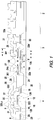
- Figure 1 is a cross sectional area of an integrated circuit with a programmable diode.
- Figures 2(a) - (j) show a series of sequential steps for forming conductive and insulating layers on top of the substrate in order to provide the device shown in Fig. 1.
- Figure 3 is a cross section of a second embodiment of the invention.
- Figure 4 is a cross section of a third embodiment of the invention.
- Figure 1 illustrates an integrated circuit with a transistor 4, resistor 2, and a diode 3 constructed on a substrate of monocrystalline silicon 12.
- the n-type substrate 12 has a p-type layer 16. Within the layer 16 are highly doped n-type regions 18.
- the p-n type diode 3 having a highly doped n-type region 18a surrounded by the p-type layer 16 is formed in the integrated circuit 10.
- the diode has first and second metal contact terminals 32a, 34a, respectively.
- a thick field oxide layer 20 separates the device 3, 4 from each other and from adjacent devices.
- the first level metal contact layer 32 has an aluminum layer 31 in mechanical and electrical contact with a conductive barrier layer 30 that is also in mechanical and electrical contact with an optional silicide layer 128 that is also in mechanical and electrical contact with the upper surface of the monosilicon 26 substrate 12 and in contact with the p layer 16.
- First level metal layer 32 provides contacts 32a, 32b, 32c . . . 32n.
- the barrier layer 30 is typically comprised of a barrier metal material such as titanium tungsten (TiW). Other barrier metals may include, but are not limited to TiN and Ti.
- the substrate 12 has a thin, first oxide layer 8. On first oxide 8 there is a polysilicon layer 22.
- the polysilicon layer 22 is patterned to define apertures for the diode 3 and the gate 22b of the transistor 4.
- the polysilicon layer 22 in the region of diode 3 has an opening a.
- the opening a is less than the width of the n+ diffusion region 18a, whose width is b.
- the opening a in polysilicon layer 22 defines the diffusion region 18a of diode 3.
- Bach polysilicon layer portion 22a, 22a' has a width c which overlaps portions d of the n+ region 18a.
- the remainders of the polysilicon layer portions 22a, 22a' are disposed over the p-region 16, and oxide 20.
- Oxide layer 24 is opened to silicide the polysilicon and the substrate.
- Oxide spacers 9 enclose the sidewalls of the patterned polysilicon 22a, 22a'.
- a third oxide layer 26 has sidewalls 25 that initially define a first level metal aperture opening. Adjacent to sidewalls 25 are residual portions 301 (stringers) of the first metal layer.
- First metal layer 32 provides contacts 32a, 32b, ... 32n.
- a fourth oxide layer 28 is disposed over the residual portions 301 of the first metal layer and the third oxide layer 26 and metal contacts 32n. The fourth oxide layer 28 extends partially over the polysilicon layer 22.
- the final second aperture for metal contacts 34n is defined by sidewalls 27 in the fourth oxide 28.
- the sidewalls 27 together with the polysilicon 22 define a stepped aperture to receive the second level metal 34, which is preferably aluminum.
- the second level metal 34 fills the aperture defined by sidewalls 27 and contacts the surface of the substrate 12 in the center of the region defined by n+ diffusion 18.
- a silicide layer 128 is provided on top of the polysilicon layer 22 and portions of surface 12. Silicide layer 128 will allow the migration of the second metal contact 34 into the silicon 12.
- Figure 1 shows a diode 3 defined by a first metal contact 15 32a, a p region 16, ann region 18a, and a second metal contact 34a.
- the diode 3 In its normal state as shown in Figure 1, if the diode 3 is back biased, it appears to be an open circuit in the integrated circuit 10. However, when the diode 3 is programmed it appears to be a short circuit or at least a very low resistive path. Programming is accomplished by passing a relatively high current in the order of 100 milliamps at a relatively high voltage on the order of 10 volts through the second metal contact 34a.
- the polysilicon layer 22 extends over a portion of the n region 18a as well as a portion of the p region 16.
- the aperture in fourth oxide 28 is formed to receive metal contact 34a and is wider than the opening a in polysilicon layer 22.
- the opening a in the polysilicon layer 22 is less than the width b of the n+ region 18.
- the shape of the metal contact 34 is generally reduced in diameter as the metal 34 nears the surface 12 of the silicon.
- the substrate 12 is a n single crystal silicon substrate with a p-type surface region 16. Thick oxide regions 20 separate adjacent device regions.
- a thin, first oxide layer 8 is formed upon which an n-doped polysilicon layer 22 is uniformly deposited.
- a layer of photoresist 50 is uniformly deposited and patterned to define the polysilicon 22 layer in Figure 2 (b). The areas of the polysilicon layer 22 not covered by photoresist 50 are suitably etched to the thin oxide layer 8 and provide the intermediate structure shown in Figure 2(c).
- polysilicon layer 22 is patterned to define a surface contact region 44 on the surface of substrate 12.
- the n region 18 is implanted (see arrows) or diffused via an implant or diffusion 52 into the surface of the substrate 12 using masking layer 51.
- the polysilicon layer 22 is self-aligned with the n region 18. The spacing a between the polysilicon strips 22a, 22a' defines the n region 18 which subsequently diffuses laterally. Thereafter the masking layer 51 is removed and a conformal second layer 24 of silicon dioxide is deposited as shown in Figure 2(d).
- the second silicon dioxide layer 24 and portions of layer 8 are etched to expose the surface of poly layer 22 and the surface of substrate 12.
- the polysilicon 22 and the substrate 12 are silicided to provide a silicide layer 128 as shown in Figure 2(e).
- a third silicon dioxide layer 26 is deposited and coated with photoresist 53 which is patterned to define first and second contact apertures 60, 61, respectively.
- the third oxide layer 26 is suitably patterned and etched to expose the silicided surface 128 of polysilicon 22 and of the silicon in the regions of the first and second apertures 60, 61, respectively.
- Figure 2(g) shows a first metal layer 32 with barrier layer 30 and metal layer 31 is deposited over the surface of the substrate 12, patterned and etched, as shown in Figure 2(h) to provide the first metal contact 32a in the first aperture 60.
- the metal layer 31 is aluminum and the etch stops on the barrier layer 30.
- the barrier layer is etched, stopping on the silicide 128.
- the second aperture 61 has the first metal 32 removed except for metal stringers 301. Stringers 301 remain because it is difficult to remove residual first metal layer 32 without significant overetch in second aperture 61. Overetch of layer 32 is undesirable and the presence of stringers 301 is not detrimental to the process or the diode 3 since stringers 301 are laterally displaced from the active programming area. This is an advantage of using polysilicon 22 as part of the diode 3 structure.
- a fourth oxide layer 28 is deposited over the substrate 12 in order to isolate the first metal layer 32 from the rest of the circuit.
- the layer 28 is then suitably patterned and etched to stop on the silicide 128 and to open the second aperture 61.
- a second level metal 34 typically aluminum, is uniformly deposited over the entire surface of the substrate and second level metal layer 34 is then patterned to form second level metal contacts 34a, 34b ... 34n. The second level metal 34 is etched to stop on fourth level oxide 28.
- the layer of polysilicon 22 is absent and the first level metal stringers 301 contact the silicide areas 128 and adhere to the adjacent oxide 26. Alternately, the silicide 128 can be removed. With such a structure, the process is simpler since the polysilicon layer 22 is omitted. However, the stringers 301 give the resulting diode 3 a wider programming voltage variation.
- FIG 4 a third embodiment is shown.
- the opening A1 in polysilicon layer 22 is enlarged so that opening A2 in the fourth oxide layer 28 can accommodate the second level metal layer 34.
- the second level metal layer 34 is nested within the opening A1 of polysilicon layer 22.
- the polysilicon layer 22 is electrically isolated from second level metal layer 34 by the fourth oxide layer 28.
- the tiered structure shown in Figure 4 for layer 34 provides good step coverage so long as opening A2 is large enough. Since sidewall spacer oxide 24 is thin, it may be etched away during earlier oxide etch steps, e.g. during the etching of third oxide layer 26.
- the structure of Figure 4 also protects the non-silicided surface areas 40 of the substrate 12.
- the areas 40 located between the edges of the polysilicon layer 22 and the silicide surface 128, have a low selectivity to an oxide etch. If sidewall spacer 24 is removed by an earlier oxide etch, an overetch of fourth oxide layer 28 could damage the junction 18 in the areas 40. Damage to areas 40 may result in excessive diode leakage. However, the opening A1 in polysilicon layer 22 is large enough to accept a fourth oxide layer 28 that is thick enough to protect areas 40.
- An integrated circuit 10 has a programmable Zener diode with diffusion regions 18 and 16 and metal contacts 34 and 32.
- a barrier metal 30 is disposed between one contact 32 and the substrate 12; another contact region 44 has no barrier metal on its surface.
- a polysilicon layer 22 is self-aligned with surface regions 44 and diffusion region 18.
- a silicide layer 128 may be used on the polysilicon layer 22 and on surface region 44.
Landscapes
- Semiconductor Memories (AREA)
- Internal Circuitry In Semiconductor Integrated Circuit Devices (AREA)
Applications Claiming Priority (2)
| Application Number | Priority Date | Filing Date | Title |
|---|---|---|---|
| US08/310,280 US5648678A (en) | 1994-09-21 | 1994-09-21 | Programmable element in barrier metal device |
| US310280 | 1994-09-21 |
Publications (2)
| Publication Number | Publication Date |
|---|---|
| EP0703624A1 true EP0703624A1 (fr) | 1996-03-27 |
| EP0703624B1 EP0703624B1 (fr) | 2000-07-19 |
Family
ID=23201779
Family Applications (1)
| Application Number | Title | Priority Date | Filing Date |
|---|---|---|---|
| EP95401944A Expired - Lifetime EP0703624B1 (fr) | 1994-09-21 | 1995-08-24 | Elément programmable dans les dispositifs à couches-barrière métalliques et procédé |
Country Status (3)
| Country | Link |
|---|---|
| US (1) | US5648678A (fr) |
| EP (1) | EP0703624B1 (fr) |
| DE (1) | DE69518047T2 (fr) |
Families Citing this family (9)
| Publication number | Priority date | Publication date | Assignee | Title |
|---|---|---|---|---|
| US5814887A (en) * | 1996-01-26 | 1998-09-29 | Nippon Steel Corporation | Semiconductor device and production method thereof |
| JP3799714B2 (ja) * | 1997-02-17 | 2006-07-19 | ソニー株式会社 | 半導体装置 |
| US6140692A (en) | 1997-05-29 | 2000-10-31 | Micron Technology, Inc. | Isolated anti-fuse structure and method for fabricating same |
| US5888894A (en) * | 1997-11-07 | 1999-03-30 | Integrated Silicon Solution, Inc. | Method for reducing stray conductive material near vertical surfaces in semiconductor manufacturing processes |
| US6051486A (en) * | 1997-12-18 | 2000-04-18 | Advanced Miero Devices | Method and structure for replaceable gate electrode in insulated gate field effect transistors |
| US6262460B1 (en) * | 2000-01-07 | 2001-07-17 | National Semiconductor Corporation | Long channel MOS transistor that utilizes a schottky diode to increase the threshold voltage of the transistor |
| US6440781B1 (en) * | 2001-06-06 | 2002-08-27 | National Semiconductor Corporation | Method of adding bias-independent aluminum bridged anti-fuses to a tungsten plug process |
| US6563189B1 (en) * | 2001-06-06 | 2003-05-13 | National Semiconductor Corporation | Method of adding Zener zap aluminum bridged anti-fuses to a tungsten plug process |
| US6770531B2 (en) * | 2001-06-30 | 2004-08-03 | Intel Corporation | Adhesive material for programmable device |
Citations (3)
| Publication number | Priority date | Publication date | Assignee | Title |
|---|---|---|---|---|
| US4312046A (en) * | 1979-10-04 | 1982-01-19 | Harris Corporation | Vertical fuse and method of fabrication |
| EP0509631A1 (fr) * | 1991-04-18 | 1992-10-21 | Actel Corporation | Antifusibles avec superfixie minimale |
| EP0562996A1 (fr) * | 1992-03-27 | 1993-09-29 | International Business Machines Corporation | Antifusible électriquement programmable utilisant une pénétration métallique d'une jonction |
Family Cites Families (6)
| Publication number | Priority date | Publication date | Assignee | Title |
|---|---|---|---|---|
| US4569120A (en) * | 1983-03-07 | 1986-02-11 | Signetics Corporation | Method of fabricating a programmable read-only memory cell incorporating an antifuse utilizing ion implantation |
| US5021840A (en) * | 1987-08-18 | 1991-06-04 | Texas Instruments Incorporated | Schottky or PN diode with composite sidewall |
| US5270569A (en) * | 1990-01-24 | 1993-12-14 | Harris Corporation | Method and device in which bottoming of a well in a dielectrically isolated island is assured |
| US5272101A (en) * | 1990-04-12 | 1993-12-21 | Actel Corporation | Electrically programmable antifuse and fabrication processes |
| US5270265A (en) * | 1992-09-01 | 1993-12-14 | Harris Corporation | Stress relief technique of removing oxide from surface of trench-patterned semiconductor-on-insulator structure |
| US5272104A (en) * | 1993-03-11 | 1993-12-21 | Harris Corporation | Bonded wafer process incorporating diamond insulator |
-
1994
- 1994-09-21 US US08/310,280 patent/US5648678A/en not_active Expired - Lifetime
-
1995
- 1995-08-24 DE DE69518047T patent/DE69518047T2/de not_active Expired - Fee Related
- 1995-08-24 EP EP95401944A patent/EP0703624B1/fr not_active Expired - Lifetime
Patent Citations (3)
| Publication number | Priority date | Publication date | Assignee | Title |
|---|---|---|---|---|
| US4312046A (en) * | 1979-10-04 | 1982-01-19 | Harris Corporation | Vertical fuse and method of fabrication |
| EP0509631A1 (fr) * | 1991-04-18 | 1992-10-21 | Actel Corporation | Antifusibles avec superfixie minimale |
| EP0562996A1 (fr) * | 1992-03-27 | 1993-09-29 | International Business Machines Corporation | Antifusible électriquement programmable utilisant une pénétration métallique d'une jonction |
Also Published As
| Publication number | Publication date |
|---|---|
| US5648678A (en) | 1997-07-15 |
| DE69518047T2 (de) | 2001-01-11 |
| EP0703624B1 (fr) | 2000-07-19 |
| DE69518047D1 (de) | 2000-08-24 |
Similar Documents
| Publication | Publication Date | Title |
|---|---|---|
| US4651409A (en) | Method of fabricating a high density, low power, merged vertical fuse/bipolar transistor | |
| US5163180A (en) | Low voltage programming antifuse and transistor breakdown method for making same | |
| US4748490A (en) | Deep polysilicon emitter antifuse memory cell | |
| CA1181848A (fr) | Cellule programmable pour reseaux electroniques programmables | |
| CA1211561A (fr) | Memoire morte programmable et methode de fabrication d'une telle structure | |
| US5311039A (en) | PROM and ROM memory cells | |
| US5352923A (en) | Trench resistors for integrated circuits | |
| EP0365932A1 (fr) | Dispositif semi-conducteur | |
| JP2000100979A (ja) | 電気的にプログラム可能な不揮発性メモリセル装置及びこの不揮発性メモリセル装置を製造する方法 | |
| US5436496A (en) | Vertical fuse device | |
| EP0729647A1 (fr) | Grille a ouvertures en forme de diamant pour groupement de transistors mos cellulaire | |
| US6013940A (en) | Poly-crystalline silicon film ladder resistor | |
| JPH10506755A (ja) | エンハンストドリフト領域を備える高電圧横型dmosデバイス | |
| NL8003612A (nl) | Werkwijze ter vervaardiging van een halfgeleider- inrichting en halfgeleiderinrichting vervaardigd door toepassing van deze werkwijze. | |
| EP1233453A2 (fr) | Circuit intégré semi-conducteur comprenant un anti-fusible, procédé de fabrication, et procédé d'écriture de données dans le même | |
| EP0703624B1 (fr) | Elément programmable dans les dispositifs à couches-barrière métalliques et procédé | |
| US4635345A (en) | Method of making an intergrated vertical NPN and vertical oxide fuse programmable memory cell | |
| EP0172193B1 (fr) | Cellule de memoire morte programmable et son procede de fabrication | |
| US5852323A (en) | Electrically programmable antifuse using metal penetration of a P-N junction | |
| US4692787A (en) | Programmable read-only-memory element with polycrystalline silicon layer | |
| GB2188778A (en) | Resistor for semiconductor IC devices | |
| EP0018173A1 (fr) | Dispositif de mémoire morte programmable | |
| US4898838A (en) | Method for fabricating a poly emitter logic array | |
| EP0621631B1 (fr) | Méthode de formation de résistances pour circuits intégrés, en utilisant des tranchées | |
| EP0041770A2 (fr) | Elément de mémoire morte programmable et procédé pour sa fabrication |
Legal Events
| Date | Code | Title | Description |
|---|---|---|---|
| PUAI | Public reference made under article 153(3) epc to a published international application that has entered the european phase |
Free format text: ORIGINAL CODE: 0009012 |
|
| AK | Designated contracting states |
Kind code of ref document: A1 Designated state(s): DE FR GB IT NL SE |
|
| 17P | Request for examination filed |
Effective date: 19960614 |
|
| 17Q | First examination report despatched |
Effective date: 19980401 |
|
| GRAG | Despatch of communication of intention to grant |
Free format text: ORIGINAL CODE: EPIDOS AGRA |
|
| GRAG | Despatch of communication of intention to grant |
Free format text: ORIGINAL CODE: EPIDOS AGRA |
|
| GRAH | Despatch of communication of intention to grant a patent |
Free format text: ORIGINAL CODE: EPIDOS IGRA |
|
| GRAH | Despatch of communication of intention to grant a patent |
Free format text: ORIGINAL CODE: EPIDOS IGRA |
|
| RAP1 | Party data changed (applicant data changed or rights of an application transferred) |
Owner name: INTERSIL CORPORATION |
|
| GRAA | (expected) grant |
Free format text: ORIGINAL CODE: 0009210 |
|
| AK | Designated contracting states |
Kind code of ref document: B1 Designated state(s): DE FR GB IT NL SE |
|
| ET | Fr: translation filed | ||
| REF | Corresponds to: |
Ref document number: 69518047 Country of ref document: DE Date of ref document: 20000824 |
|
| ITF | It: translation for a ep patent filed | ||
| PLBE | No opposition filed within time limit |
Free format text: ORIGINAL CODE: 0009261 |
|
| STAA | Information on the status of an ep patent application or granted ep patent |
Free format text: STATUS: NO OPPOSITION FILED WITHIN TIME LIMIT |
|
| 26N | No opposition filed | ||
| REG | Reference to a national code |
Ref country code: GB Ref legal event code: IF02 |
|
| PGFP | Annual fee paid to national office [announced via postgrant information from national office to epo] |
Ref country code: FR Payment date: 20020731 Year of fee payment: 8 |
|
| PGFP | Annual fee paid to national office [announced via postgrant information from national office to epo] |
Ref country code: NL Payment date: 20020801 Year of fee payment: 8 |
|
| PGFP | Annual fee paid to national office [announced via postgrant information from national office to epo] |
Ref country code: GB Payment date: 20020821 Year of fee payment: 8 |
|
| PGFP | Annual fee paid to national office [announced via postgrant information from national office to epo] |
Ref country code: DE Payment date: 20020830 Year of fee payment: 8 |
|
| PG25 | Lapsed in a contracting state [announced via postgrant information from national office to epo] |
Ref country code: GB Free format text: LAPSE BECAUSE OF NON-PAYMENT OF DUE FEES Effective date: 20030824 |
|
| PG25 | Lapsed in a contracting state [announced via postgrant information from national office to epo] |
Ref country code: NL Free format text: LAPSE BECAUSE OF NON-PAYMENT OF DUE FEES Effective date: 20040301 |
|
| PGFP | Annual fee paid to national office [announced via postgrant information from national office to epo] |
Ref country code: SE Payment date: 20040301 Year of fee payment: 9 |
|
| PG25 | Lapsed in a contracting state [announced via postgrant information from national office to epo] |
Ref country code: DE Free format text: LAPSE BECAUSE OF NON-PAYMENT OF DUE FEES Effective date: 20040302 |
|
| GBPC | Gb: european patent ceased through non-payment of renewal fee | ||
| PG25 | Lapsed in a contracting state [announced via postgrant information from national office to epo] |
Ref country code: FR Free format text: LAPSE BECAUSE OF NON-PAYMENT OF DUE FEES Effective date: 20040430 |
|
| NLV4 | Nl: lapsed or anulled due to non-payment of the annual fee |
Effective date: 20040301 |
|
| REG | Reference to a national code |
Ref country code: FR Ref legal event code: ST |
|
| PG25 | Lapsed in a contracting state [announced via postgrant information from national office to epo] |
Ref country code: SE Free format text: LAPSE BECAUSE OF NON-PAYMENT OF DUE FEES Effective date: 20040825 |
|
| EUG | Se: european patent has lapsed | ||
| PG25 | Lapsed in a contracting state [announced via postgrant information from national office to epo] |
Ref country code: IT Free format text: LAPSE BECAUSE OF NON-PAYMENT OF DUE FEES;WARNING: LAPSES OF ITALIAN PATENTS WITH EFFECTIVE DATE BEFORE 2007 MAY HAVE OCCURRED AT ANY TIME BEFORE 2007. THE CORRECT EFFECTIVE DATE MAY BE DIFFERENT FROM THE ONE RECORDED. Effective date: 20050824 |