EP0703629A2 - Transistor à effet de champ vertical de puissance - Google Patents
Transistor à effet de champ vertical de puissance Download PDFInfo
- Publication number
- EP0703629A2 EP0703629A2 EP95113532A EP95113532A EP0703629A2 EP 0703629 A2 EP0703629 A2 EP 0703629A2 EP 95113532 A EP95113532 A EP 95113532A EP 95113532 A EP95113532 A EP 95113532A EP 0703629 A2 EP0703629 A2 EP 0703629A2
- Authority
- EP
- European Patent Office
- Prior art keywords
- zone
- effect transistor
- gate
- vertical field
- transistor according
- Prior art date
- Legal status (The legal status is an assumption and is not a legal conclusion. Google has not performed a legal analysis and makes no representation as to the accuracy of the status listed.)
- Ceased
Links
Images


Classifications
-
- H—ELECTRICITY
- H10—SEMICONDUCTOR DEVICES; ELECTRIC SOLID-STATE DEVICES NOT OTHERWISE PROVIDED FOR
- H10D—INORGANIC ELECTRIC SEMICONDUCTOR DEVICES
- H10D30/00—Field-effect transistors [FET]
- H10D30/60—Insulated-gate field-effect transistors [IGFET]
- H10D30/611—Insulated-gate field-effect transistors [IGFET] having multiple independently-addressable gate electrodes influencing the same channel
- H10D30/615—Insulated-gate field-effect transistors [IGFET] having multiple independently-addressable gate electrodes influencing the same channel comprising a MOS gate electrode and at least one non-MOS gate electrode
-
- H—ELECTRICITY
- H10—SEMICONDUCTOR DEVICES; ELECTRIC SOLID-STATE DEVICES NOT OTHERWISE PROVIDED FOR
- H10D—INORGANIC ELECTRIC SEMICONDUCTOR DEVICES
- H10D12/00—Bipolar devices controlled by the field effect, e.g. insulated-gate bipolar transistors [IGBT]
- H10D12/01—Manufacture or treatment
- H10D12/031—Manufacture or treatment of IGBTs
-
- H—ELECTRICITY
- H10—SEMICONDUCTOR DEVICES; ELECTRIC SOLID-STATE DEVICES NOT OTHERWISE PROVIDED FOR
- H10D—INORGANIC ELECTRIC SEMICONDUCTOR DEVICES
- H10D30/00—Field-effect transistors [FET]
- H10D30/80—FETs having rectifying junction gate electrodes
- H10D30/83—FETs having PN junction gate electrodes
- H10D30/831—Vertical FETs having PN junction gate electrodes
-
- H—ELECTRICITY
- H10—SEMICONDUCTOR DEVICES; ELECTRIC SOLID-STATE DEVICES NOT OTHERWISE PROVIDED FOR
- H10D—INORGANIC ELECTRIC SEMICONDUCTOR DEVICES
- H10D62/00—Semiconductor bodies, or regions thereof, of devices having potential barriers
- H10D62/80—Semiconductor bodies, or regions thereof, of devices having potential barriers characterised by the materials
- H10D62/83—Semiconductor bodies, or regions thereof, of devices having potential barriers characterised by the materials being Group IV materials, e.g. B-doped Si or undoped Ge
- H10D62/832—Semiconductor bodies, or regions thereof, of devices having potential barriers characterised by the materials being Group IV materials, e.g. B-doped Si or undoped Ge being Group IV materials comprising two or more elements, e.g. SiGe
- H10D62/8325—Silicon carbide
-
- H—ELECTRICITY
- H10—SEMICONDUCTOR DEVICES; ELECTRIC SOLID-STATE DEVICES NOT OTHERWISE PROVIDED FOR
- H10D—INORGANIC ELECTRIC SEMICONDUCTOR DEVICES
- H10D62/00—Semiconductor bodies, or regions thereof, of devices having potential barriers
- H10D62/80—Semiconductor bodies, or regions thereof, of devices having potential barriers characterised by the materials
- H10D62/85—Semiconductor bodies, or regions thereof, of devices having potential barriers characterised by the materials being Group III-V materials, e.g. GaAs
- H10D62/8503—Nitride Group III-V materials, e.g. AlN or GaN
Definitions
- the invention relates to a vertical field effect transistor according to the preamble of claim 1 and a method for its production.
- the doping of the drift zone between gate and drain determines the maximum reverse voltage. High reverse voltages require low doping of the drift zone, which is associated with a high drift zone resistance.
- the invention has for its object to develop a vertical field effect transistor of high dielectric strength of the type mentioned so that the constriction of the channel zone begins even at low gate voltages and that the resistance of the channel zone is within the usual range with this measure.
- Areas of application of the invention are high-blocking components for drive technology. Such components can be used, for example, for converters in electric drives.
- the essence of the invention is that the gate region in the vertical component is initially formed laterally and has a large horizontal spread. This lateral channel zone is blocked off particularly well by the buried gate. Below that is the drift zone, which receives the reverse voltage.
- the dielectric strength and the on-resistance of the material are of crucial importance for the drift zone. Therefore, semiconducting materials with a large band gap (SiC, diamond, AlN, GaN, BN) are favorable, which achieve high breakdown voltages with doping that is considerably higher than that of silicon.
- the substrate should be as low-resistance as possible. Either the same material as for the drift zone or silicon can be used as the material for the substrate.
- the vertical field effect transistor 1 is shown in FIGS. 1 and 2 and consists essentially of the substrate 2 (n+- or p+- doped), on the underside of which the drain contact 3 is attached, the drift zone 4, which has an n ⁇ Doping, the gate 7, which extends only partially over the drift zone 4 and which is p+-doped, the n-doped channel zone 5 and the source region 6 embedded in this channel zone, which is n+-doped.
- the drift zone material can be semiconducting diamond, AlN, GaN, another nitride or SiC. The material's dielectric strength is the decisive factor.
- the channel zone 5 is preferably made of the same material as the drift zone 4, but the material must be selected so that the majority charge carriers have the highest possible mobility there.
- a hexagonal polytype of SiC (4H or 6H) is used as the material for the drift zone.
- the dimensions are entered in Fig. 2.
- the drift zone 4 extends over the entire width of the silicon carbide disk.
- the gate 7, like the entire component, is only shown in half in FIG. 2. Its thickness is b 0.5 ⁇ m.
- the channel zone preferably consists of 3C-SiC, which has been grown heteroepitaxially.
- FIG. 8 shows computer simulation results for the component shown in FIG. 2.
- the drain current density as a function of the drain-source voltage U D for different gate voltages U g is plotted in both partial images.
- a breakdown voltage of can be read from the left partial image (semi-logarithmic representation) approx. 4500 V.
- the saturation behavior of the drain current is also clear.
- the voltage gain is about 1000. If one assumes a maximum permissible power density of approx. 100 W / cm, the maximum current densities are approx. 50 A / cm.
- drift zone doping N D1 It is generally known that other breakdown voltages can be set by appropriately adapting the drift zone doping N D1 .
- cell-shaped arrangements of rotationally symmetrical components are available.
- the substrate is p+-doped and thus further reduces the on-resistance as a drain-side emitter due to charge carrier flooding of the drift zone.
- the gate zone 7 can be supplemented by a further gate zone 17 on the surface of the component in order to better constrict the channel region (FIG. 9). In this way, the canal is constricted from both sides.
- a pn junction can be used for this.
- a further preferred structure variant would instead be a metal-insulator-semiconductor structure (MIS or MOS structure).
- MIS metal-insulator-semiconductor structure
- MOS metal-insulator-semiconductor structure
- the buried gate 7 and the source contact 8 are short-circuited, so that the constriction of the channel is essentially achieved by the surface gate zone 17.
- All semiconductors with a large band gap can be used as the material for the component.
- Such materials are e.g. As silicon carbide, AlN, GaN, BN and semiconducting diamond. These materials are used when it comes to high dielectric strength. You will generally deposited or bonded on a substrate made of the same material as the drift zone or silicon. Bonding is a process in which two semiconductor wafers are placed on top of one another and connected to one another by means of high temperature.
- SiC the starting material for the component as n als layer 4
- the doping N D1 is chosen according to the maximum reverse voltage, as is the thickness.
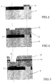
- a mask 12 made of SiO2 is applied and a p+ zone 7 is generated by ion implantation.
- the mask 12 is removed and, as shown in FIG. 4, a channel zone 5 is epitaxially deposited. Thickness and doping have to be optimized for the channel conductivity and favorable constriction or barrier properties. With SiC this can also be achieved by changing the polytype.
- the second mask 13 is then applied.
- the gate contacting is carried out as a further step. It consists in first etching a trench and sputtering on metal 11. Examples of suitable metals are titanium, Ni or NiCr. The trench is filled with an insulator 10. The second mask is then removed. This process is referred to as "lift-off" (Fig. 6).
- the next step consists in applying the third mask 16 (see FIG. 7) for the n + ion implantation in preparation for the source contact.
- the n+ layer 6 is formed.
- metal 8 is sputtered on.
- the final step is to remove the third mask; if necessary, the surface is passivated. The result is the finished component according to FIGS. 1 and 2.
- the back of the substrate is contacted in the usual way and forms the drain contact 3, which is shown schematically in FIG. 2.
Landscapes
- Junction Field-Effect Transistors (AREA)
Applications Claiming Priority (2)
| Application Number | Priority Date | Filing Date | Title |
|---|---|---|---|
| DE4430732A DE4430732C2 (de) | 1994-08-30 | 1994-08-30 | Vertikaler Feldeffekt-Transistor hoher Leistung und Verfahren zu dessen Herstellung |
| DE4430732 | 1994-08-30 |
Publications (2)
| Publication Number | Publication Date |
|---|---|
| EP0703629A2 true EP0703629A2 (fr) | 1996-03-27 |
| EP0703629A3 EP0703629A3 (fr) | 1996-11-13 |
Family
ID=6526902
Family Applications (1)
| Application Number | Title | Priority Date | Filing Date |
|---|---|---|---|
| EP95113532A Ceased EP0703629A3 (fr) | 1994-08-30 | 1995-08-29 | Transistor à effet de champ vertical de puissance |
Country Status (2)
| Country | Link |
|---|---|
| EP (1) | EP0703629A3 (fr) |
| DE (1) | DE4430732C2 (fr) |
Cited By (8)
| Publication number | Priority date | Publication date | Assignee | Title |
|---|---|---|---|---|
| EP0726604A3 (fr) * | 1995-02-08 | 1997-09-24 | Ngk Insulators Ltd | Dispositif de type MIS et méthode de fabrication |
| WO1998010468A1 (fr) * | 1996-09-05 | 1998-03-12 | Northrop Grumman Corporation | Transistors a induction statique |
| WO1998019342A1 (fr) * | 1996-10-29 | 1998-05-07 | Daimler-Benz Aktiengesellschaft | Structure a semi-conducteur pilotable a proprietes de commutation ameliorees |
| EP0869558A3 (fr) * | 1997-03-31 | 1999-07-21 | Motorola, Inc. | Transistor bipolaire à grille isolée avec un champ électrique réduit |
| WO2000003440A1 (fr) * | 1998-07-09 | 2000-01-20 | Cree, Inc. | Dispositif a semi-conducteur a grille tamponnee a canal horizontal au carbure de silicium |
| US6693322B2 (en) | 2000-07-25 | 2004-02-17 | Siced Electronics Development Gmbh & Co. Kg | Semiconductor construction with buried island region and contact region |
| EP2375451A3 (fr) * | 2004-12-01 | 2012-04-18 | Ss Sc Ip, Llc | Transistors à effet de champ à tranchée latérale dans des matériaux semi-conducteurs à bande interdite large, procédés de fabrication et circuits intégrés intégrant les transistors |
| WO2021202228A1 (fr) * | 2020-03-29 | 2021-10-07 | Power Integrations, Inc. | Transistors à effet de champ à jonction en carbure de silicium |
Family Cites Families (5)
| Publication number | Priority date | Publication date | Assignee | Title |
|---|---|---|---|---|
| FR2205749B1 (fr) * | 1972-11-09 | 1978-03-31 | Teszner Stanislas | |
| FR2303383A1 (fr) * | 1975-03-06 | 1976-10-01 | Alsthom Cgee | Transistor a effet de champ a plat |
| DE2611338C3 (de) * | 1976-03-17 | 1979-03-29 | Siemens Ag, 1000 Berlin Und 8000 Muenchen | Feldeffekttransistor mit sehr kurzer Kanallange |
| US4454523A (en) * | 1981-03-30 | 1984-06-12 | Siliconix Incorporated | High voltage field effect transistor |
| US5323040A (en) * | 1993-09-27 | 1994-06-21 | North Carolina State University At Raleigh | Silicon carbide field effect device |
-
1994
- 1994-08-30 DE DE4430732A patent/DE4430732C2/de not_active Expired - Lifetime
-
1995
- 1995-08-29 EP EP95113532A patent/EP0703629A3/fr not_active Ceased
Cited By (15)
| Publication number | Priority date | Publication date | Assignee | Title |
|---|---|---|---|---|
| US6025233A (en) * | 1995-02-08 | 2000-02-15 | Ngk Insulators, Ltd. | Method of manufacturing a semiconductor device |
| EP0726604A3 (fr) * | 1995-02-08 | 1997-09-24 | Ngk Insulators Ltd | Dispositif de type MIS et méthode de fabrication |
| US6002143A (en) * | 1995-02-08 | 1999-12-14 | Ngk Insulators, Ltd. | Hybrid vertical type power semiconductor device |
| WO1998010468A1 (fr) * | 1996-09-05 | 1998-03-12 | Northrop Grumman Corporation | Transistors a induction statique |
| WO1998019342A1 (fr) * | 1996-10-29 | 1998-05-07 | Daimler-Benz Aktiengesellschaft | Structure a semi-conducteur pilotable a proprietes de commutation ameliorees |
| EP0869558A3 (fr) * | 1997-03-31 | 1999-07-21 | Motorola, Inc. | Transistor bipolaire à grille isolée avec un champ électrique réduit |
| WO2000003440A1 (fr) * | 1998-07-09 | 2000-01-20 | Cree, Inc. | Dispositif a semi-conducteur a grille tamponnee a canal horizontal au carbure de silicium |
| US6281521B1 (en) | 1998-07-09 | 2001-08-28 | Cree Research Inc. | Silicon carbide horizontal channel buffered gate semiconductor devices |
| CN100385676C (zh) * | 1998-07-09 | 2008-04-30 | 克里公司 | 碳化硅水平沟道缓冲栅极半导体器件 |
| EP2264769A1 (fr) * | 1998-07-09 | 2010-12-22 | Cree, Inc. | Dispositif a semi-conducteur a grille tamponnee a canal horizontal au carbure de silicium |
| US6693322B2 (en) | 2000-07-25 | 2004-02-17 | Siced Electronics Development Gmbh & Co. Kg | Semiconductor construction with buried island region and contact region |
| DE10036208B4 (de) * | 2000-07-25 | 2007-04-19 | Siced Electronics Development Gmbh & Co. Kg | Halbleiteraufbau mit vergrabenem Inselgebiet und Konaktgebiet |
| EP2375451A3 (fr) * | 2004-12-01 | 2012-04-18 | Ss Sc Ip, Llc | Transistors à effet de champ à tranchée latérale dans des matériaux semi-conducteurs à bande interdite large, procédés de fabrication et circuits intégrés intégrant les transistors |
| WO2021202228A1 (fr) * | 2020-03-29 | 2021-10-07 | Power Integrations, Inc. | Transistors à effet de champ à jonction en carbure de silicium |
| US11824094B2 (en) | 2020-03-29 | 2023-11-21 | Power Integrations, Inc. | Silicon carbide junction field effect transistors |
Also Published As
| Publication number | Publication date |
|---|---|
| DE4430732C2 (de) | 1998-07-02 |
| EP0703629A3 (fr) | 1996-11-13 |
| DE4430732A1 (de) | 1996-03-28 |
Similar Documents
| Publication | Publication Date | Title |
|---|---|---|
| EP0715771B1 (fr) | TRANSISTOR SiC A EFFET DE CHAMP ET SON PROCEDE DE FABRICATION | |
| AT404525B (de) | Leistungstransistorvorrichtung und verfahren zu deren herstellung | |
| DE69414311T2 (de) | Halbleiteranordnung mit einer Bipolarfeldeffektanordnung mit isoliertem Gate | |
| DE69535441T2 (de) | Verfahren zur herstellung eines mos gesteuerten bauelements mit reduzierter maskenzahl | |
| DE69524777T2 (de) | Selbstausgerichteter feldeffekttransistor für hochfrequenzanwendungen | |
| EP0772889B1 (fr) | Composant a semi-conducteur a terminaison marginale a haut pouvoir de blocage | |
| DE69622295T2 (de) | MIS-Anordnung und Verfahren zur Herstellung | |
| DE3853778T2 (de) | Verfahren zur Herstellung eines Halbleiterbauelements. | |
| DE19702110B4 (de) | Siliziumkarbid-Halbleiterbauelement und Verfahren zu dessen Herstellung | |
| DE69412515T2 (de) | Drei-anschlussklemmen-gategesteuerte halbleiterschalteranordnung mit gleichrichtergate | |
| DE19629088A1 (de) | Vertikaler Siliziumcarbid-Feldeffekttransistor | |
| DE3688518T2 (de) | Halbleiteranordnungen mit Leitfähigkeitsmodulation. | |
| DE112011104322T5 (de) | Halbleitervorrichtung und Verfahren zur Herstellung einer Halbleitervorrichtung | |
| DE102018103849A1 (de) | Siliziumcarbid-Halbleiterbauelement mit einer in einer Grabenstruktur ausgebildeten Gateelektrode | |
| DE112017002113B4 (de) | Halbleitereinheit | |
| DE112017003513B4 (de) | Halbleitereinheit und Verfahren zur Herstellung derselben | |
| DE19641838A1 (de) | Abschlußstruktur für Halbleiterbauteile sowie Verfahren zur Herstellung derartiger Abschlußstrukturen | |
| EP0938751A1 (fr) | Structure a semi-conducteur pilotable a proprietes de commutation ameliorees | |
| DE2937261A1 (de) | Mos-feldeffekttransistor | |
| EP0006428B1 (fr) | Dispositif semiconducteur à tension de seuil constante | |
| DE4104588B4 (de) | Halbleiterbauelement mit einem Leitfähigkeitsmodulations-MISFET | |
| DE4430732C2 (de) | Vertikaler Feldeffekt-Transistor hoher Leistung und Verfahren zu dessen Herstellung | |
| DE2724165A1 (de) | Oberflaechen-feldeffekttransistorvorrichtung | |
| DE102019008556A1 (de) | Feldeffekttransistorstruktur mit isoliertem Gate mit abgeschirmter Quelle und Verfahren | |
| WO2021089230A1 (fr) | Transistor à effet de champ vertical et son procédé de formation |
Legal Events
| Date | Code | Title | Description |
|---|---|---|---|
| PUAI | Public reference made under article 153(3) epc to a published international application that has entered the european phase |
Free format text: ORIGINAL CODE: 0009012 |
|
| AK | Designated contracting states |
Kind code of ref document: A2 Designated state(s): CH DE FR GB IT LI NL SE |
|
| RIN1 | Information on inventor provided before grant (corrected) |
Inventor name: HELD, RABAN, DIPL.-PHYS. Inventor name: SCHLANGENOTTO, HEINRICH, DR. Inventor name: NIEMANN, EKKEHARD, DIPL.-PHYS. Inventor name: KOREC, JACEK, DR. Inventor name: LOOSE, WERNER, DR. |
|
| PUAL | Search report despatched |
Free format text: ORIGINAL CODE: 0009013 |
|
| AK | Designated contracting states |
Kind code of ref document: A3 Designated state(s): CH DE FR GB IT LI NL SE |
|
| 17P | Request for examination filed |
Effective date: 19970310 |
|
| 17Q | First examination report despatched |
Effective date: 19970721 |
|
| STAA | Information on the status of an ep patent application or granted ep patent |
Free format text: STATUS: THE APPLICATION HAS BEEN REFUSED |
|
| 18R | Application refused |
Effective date: 19980125 |