EP0703639B1 - Circuit électrique multicouche avec des bornes de raccordement - Google Patents
Circuit électrique multicouche avec des bornes de raccordement Download PDFInfo
- Publication number
- EP0703639B1 EP0703639B1 EP94114867A EP94114867A EP0703639B1 EP 0703639 B1 EP0703639 B1 EP 0703639B1 EP 94114867 A EP94114867 A EP 94114867A EP 94114867 A EP94114867 A EP 94114867A EP 0703639 B1 EP0703639 B1 EP 0703639B1
- Authority
- EP
- European Patent Office
- Prior art keywords
- limb
- circuit board
- bent
- printed circuit
- film circuit
- Prior art date
- Legal status (The legal status is an assumption and is not a legal conclusion. Google has not performed a legal analysis and makes no representation as to the accuracy of the status listed.)
- Expired - Lifetime
Links
Images

Classifications
-
- H—ELECTRICITY
- H01—ELECTRIC ELEMENTS
- H01R—ELECTRICALLY-CONDUCTIVE CONNECTIONS; STRUCTURAL ASSOCIATIONS OF A PLURALITY OF MUTUALLY-INSULATED ELECTRICAL CONNECTING ELEMENTS; COUPLING DEVICES; CURRENT COLLECTORS
- H01R12/00—Structural associations of a plurality of mutually-insulated electrical connecting elements, specially adapted for printed circuits, e.g. printed circuit boards [PCB], flat or ribbon cables, or like generally planar structures, e.g. terminal strips, terminal blocks; Coupling devices specially adapted for printed circuits, flat or ribbon cables, or like generally planar structures; Terminals specially adapted for contact with, or insertion into, printed circuits, flat or ribbon cables, or like generally planar structures
- H01R12/50—Fixed connections
- H01R12/51—Fixed connections for rigid printed circuits or like structures
- H01R12/55—Fixed connections for rigid printed circuits or like structures characterised by the terminals
- H01R12/58—Fixed connections for rigid printed circuits or like structures characterised by the terminals terminals for insertion into holes
- H01R12/585—Terminals having a press fit or a compliant portion and a shank passing through a hole in the printed circuit board
-
- H—ELECTRICITY
- H05—ELECTRIC TECHNIQUES NOT OTHERWISE PROVIDED FOR
- H05K—PRINTED CIRCUITS; CASINGS OR CONSTRUCTIONAL DETAILS OF ELECTRIC APPARATUS; MANUFACTURE OF ASSEMBLAGES OF ELECTRICAL COMPONENTS
- H05K3/00—Apparatus or processes for manufacturing printed circuits
- H05K3/30—Assembling printed circuits with electric components, e.g. with resistors
- H05K3/306—Assembling printed circuits with electric components, e.g. with resistors with lead-in-hole components
- H05K3/308—Adaptations of leads
-
- H—ELECTRICITY
- H01—ELECTRIC ELEMENTS
- H01R—ELECTRICALLY-CONDUCTIVE CONNECTIONS; STRUCTURAL ASSOCIATIONS OF A PLURALITY OF MUTUALLY-INSULATED ELECTRICAL CONNECTING ELEMENTS; COUPLING DEVICES; CURRENT COLLECTORS
- H01R12/00—Structural associations of a plurality of mutually-insulated electrical connecting elements, specially adapted for printed circuits, e.g. printed circuit boards [PCB], flat or ribbon cables, or like generally planar structures, e.g. terminal strips, terminal blocks; Coupling devices specially adapted for printed circuits, flat or ribbon cables, or like generally planar structures; Terminals specially adapted for contact with, or insertion into, printed circuits, flat or ribbon cables, or like generally planar structures
- H01R12/50—Fixed connections
- H01R12/51—Fixed connections for rigid printed circuits or like structures
- H01R12/55—Fixed connections for rigid printed circuits or like structures characterised by the terminals
- H01R12/57—Fixed connections for rigid printed circuits or like structures characterised by the terminals surface mounting terminals
-
- H—ELECTRICITY
- H01—ELECTRIC ELEMENTS
- H01R—ELECTRICALLY-CONDUCTIVE CONNECTIONS; STRUCTURAL ASSOCIATIONS OF A PLURALITY OF MUTUALLY-INSULATED ELECTRICAL CONNECTING ELEMENTS; COUPLING DEVICES; CURRENT COLLECTORS
- H01R13/00—Details of coupling devices of the kinds covered by groups H01R12/70 or H01R24/00 - H01R33/00
- H01R13/02—Contact members
- H01R13/04—Pins or blades for co-operation with sockets
- H01R13/05—Resilient pins or blades
-
- H—ELECTRICITY
- H01—ELECTRIC ELEMENTS
- H01R—ELECTRICALLY-CONDUCTIVE CONNECTIONS; STRUCTURAL ASSOCIATIONS OF A PLURALITY OF MUTUALLY-INSULATED ELECTRICAL CONNECTING ELEMENTS; COUPLING DEVICES; CURRENT COLLECTORS
- H01R13/00—Details of coupling devices of the kinds covered by groups H01R12/70 or H01R24/00 - H01R33/00
- H01R13/02—Contact members
- H01R13/193—Means for increasing contact pressure at the end of engagement of coupling part, e.g. zero insertion force or no friction
-
- H—ELECTRICITY
- H05—ELECTRIC TECHNIQUES NOT OTHERWISE PROVIDED FOR
- H05K—PRINTED CIRCUITS; CASINGS OR CONSTRUCTIONAL DETAILS OF ELECTRIC APPARATUS; MANUFACTURE OF ASSEMBLAGES OF ELECTRICAL COMPONENTS
- H05K2201/00—Indexing scheme relating to printed circuits covered by H05K1/00
- H05K2201/10—Details of components or other objects attached to or integrated in a printed circuit board
- H05K2201/10227—Other objects, e.g. metallic pieces
- H05K2201/1034—Edge terminals, i.e. separate pieces of metal attached to the edge of the printed circuit board [PCB]
-
- H—ELECTRICITY
- H05—ELECTRIC TECHNIQUES NOT OTHERWISE PROVIDED FOR
- H05K—PRINTED CIRCUITS; CASINGS OR CONSTRUCTIONAL DETAILS OF ELECTRIC APPARATUS; MANUFACTURE OF ASSEMBLAGES OF ELECTRICAL COMPONENTS
- H05K2201/00—Indexing scheme relating to printed circuits covered by H05K1/00
- H05K2201/10—Details of components or other objects attached to or integrated in a printed circuit board
- H05K2201/10613—Details of electrical connections of non-printed components, e.g. special leads
- H05K2201/10742—Details of leads
- H05K2201/1075—Shape details
- H05K2201/10757—Bent leads
- H05K2201/10765—Leads folded back, i.e. bent with an angle of 180 deg
-
- H—ELECTRICITY
- H05—ELECTRIC TECHNIQUES NOT OTHERWISE PROVIDED FOR
- H05K—PRINTED CIRCUITS; CASINGS OR CONSTRUCTIONAL DETAILS OF ELECTRIC APPARATUS; MANUFACTURE OF ASSEMBLAGES OF ELECTRICAL COMPONENTS
- H05K2201/00—Indexing scheme relating to printed circuits covered by H05K1/00
- H05K2201/10—Details of components or other objects attached to or integrated in a printed circuit board
- H05K2201/10613—Details of electrical connections of non-printed components, e.g. special leads
- H05K2201/10742—Details of leads
- H05K2201/1075—Shape details
- H05K2201/10878—Means for retention of a lead in a hole
-
- H—ELECTRICITY
- H05—ELECTRIC TECHNIQUES NOT OTHERWISE PROVIDED FOR
- H05K—PRINTED CIRCUITS; CASINGS OR CONSTRUCTIONAL DETAILS OF ELECTRIC APPARATUS; MANUFACTURE OF ASSEMBLAGES OF ELECTRICAL COMPONENTS
- H05K3/00—Apparatus or processes for manufacturing printed circuits
- H05K3/36—Assembling printed circuits with other printed circuits
- H05K3/366—Assembling printed circuits with other printed circuits substantially perpendicularly to each other
Definitions
- the invention relates to a layer circuit with at least a series of terminals for connection to metallized Holes on a circuit board, the terminals on the one side over a pocket-shaped clamping contour with connection surfaces the layer circuit are connected and on the other side for connection to the printed circuit board in the connection to a widening a band-shaped comparatively narrower
- Such a layer circuit is known from EP-0 148 461 B1 known.
- the present invention is therefore based on the object an improved layer circuit of the above Way of creating.
- this object is achieved in that the Material thickness of the bent connection pieces in the bending area is reduced by about 50%.
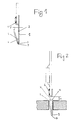
- Figure 1 is in a belonging to the terminal Clamping contour 6 soldered layer circuit shown. Recognizable the material thinning in the bending area 3 is opposite the cross-sectional thickness 2 of the remaining connector 1 with V-shape 4. With a tin layer thickness 5 of more than 10 ⁇ m, those when dip-soldering the clamping contours 6 or connection clips the layer circuit is created in the area of the connection pins, is an inner bending radius due to the changed cross-section less than 0, lmm possible. This creates such a small tapered outer radius 7, so that a desired Insertion aid and a low insertion force in the case of circuit board holes given with a diameter of less than 1.0mm is.
- connections are up to the "stand off" (s) in the plated-through z.
- B an average of 0.9mm PCB holes inserted.
- the crowned inwardly shaped end portion 8 of the free spring leg is defined below the hole edge 9 and prevents thus the otherwise disruptive driving force. In this position can be transported and wave soldered without the Circuit changed its position to the circuit board.
- the deformation path f of the spring indicated in FIG elastic material range. This is a multiple plug possible under the required criteria.
- Figure 5 shows the possible application of this invention to dual in-line circuits for the purpose of contacting as in the figures 3 and 4 or for mounting during transport and soldering in Circuit boards.
Landscapes
- Engineering & Computer Science (AREA)
- Manufacturing & Machinery (AREA)
- Microelectronics & Electronic Packaging (AREA)
- Coupling Device And Connection With Printed Circuit (AREA)
- Multi-Conductor Connections (AREA)
- Parts Printed On Printed Circuit Boards (AREA)
Claims (4)
- Circuit électrique multicouche avec au moins une rangée de bornes de raccordement servant à la liaison avec des trous métallisés d'un circuit imprimé, les bornes de raccordement étant reliées à des surfaces de connexion du circuit électrique multicouche, sur un côté, par le biais d'un contour de borne (6) en forme de poche et étant pourvues, sur l'autre côté, en vue de la liaison avec le circuit imprimé, succédant à un élargissement, d'un élément de raccordement (1) relativement plus étroit en forme de bande, et où, en vue de la mise en contact par enfichage dans les trous du circuit imprimé, au moins un des éléments de raccordement (1) est plié en forme de V de manière à former un ressort avec une branche libre et une branche reliée à l'élargissement, le rayon de courbure étant nettement plus petit que le diamètre du trou correspondant du circuit imprimé, caractérisé en ce que l'épaisseur de matériau des éléments de raccordement (1) pliés est réduite d'à peu près 50% dans la zone de pliage (3).
- Circuit électrique multicouche selon la revendication 1, dans lequel l'élément de raccordement (1) est exécuté avec un rayon de courbure interne inférieur à 0,1 mm et un rayon externe (7) se terminant en pointe et qui est, en conséquence, petit.
- Circuit électrique multicouche selon la revendication 1 ou 2, dans lequel la zone d'extrémité (8) de la branche libre est exécutée de manière bombée avec une extrémité de branche dirigée à l'intérieur vers l'autre branche.
- Circuit électrique multicouche selon la revendication 3, dans lequel la zone d'extrémité (8) est bombée à un tel point vers l'intérieur que l'extrémité de la branche est appuyée sur l'autre branche.
Priority Applications (5)
| Application Number | Priority Date | Filing Date | Title |
|---|---|---|---|
| EP94114867A EP0703639B1 (fr) | 1994-09-21 | 1994-09-21 | Circuit électrique multicouche avec des bornes de raccordement |
| DE59405595T DE59405595D1 (de) | 1994-09-21 | 1994-09-21 | Schichtschaltung mit Anschlussklemmen |
| AT94114867T ATE164706T1 (de) | 1994-09-21 | 1994-09-21 | Schichtschaltung mit anschlussklemmen |
| US08/426,221 US5635758A (en) | 1994-09-21 | 1995-04-21 | Film IC with connection terminals |
| CN95116876A CN1045694C (zh) | 1994-09-21 | 1995-09-21 | 带接线卡头的薄膜电路 |
Applications Claiming Priority (1)
| Application Number | Priority Date | Filing Date | Title |
|---|---|---|---|
| EP94114867A EP0703639B1 (fr) | 1994-09-21 | 1994-09-21 | Circuit électrique multicouche avec des bornes de raccordement |
Publications (2)
| Publication Number | Publication Date |
|---|---|
| EP0703639A1 EP0703639A1 (fr) | 1996-03-27 |
| EP0703639B1 true EP0703639B1 (fr) | 1998-04-01 |
Family
ID=8216304
Family Applications (1)
| Application Number | Title | Priority Date | Filing Date |
|---|---|---|---|
| EP94114867A Expired - Lifetime EP0703639B1 (fr) | 1994-09-21 | 1994-09-21 | Circuit électrique multicouche avec des bornes de raccordement |
Country Status (5)
| Country | Link |
|---|---|
| US (1) | US5635758A (fr) |
| EP (1) | EP0703639B1 (fr) |
| CN (1) | CN1045694C (fr) |
| AT (1) | ATE164706T1 (fr) |
| DE (1) | DE59405595D1 (fr) |
Families Citing this family (10)
| Publication number | Priority date | Publication date | Assignee | Title |
|---|---|---|---|---|
| US6542122B1 (en) * | 2001-10-16 | 2003-04-01 | Telefonaktiebolaget Lm Ericsson (Publ) | Patch antenna precision connection |
| DE102004027602A1 (de) * | 2004-06-05 | 2006-01-05 | Hella Kgaa Hueck & Co. | Scheinwerfer für Fahrzeuge |
| TWI387411B (zh) * | 2007-02-28 | 2013-02-21 | Finisar Corp | 印刷電路板及捲帶系統 |
| DE102007014356A1 (de) * | 2007-03-26 | 2008-10-02 | Robert Bosch Gmbh | Pin zum Einsetzen in eine Aufnahmeöffnung einer Leiterplatte und Verfahren zum Einsetzen eines Pin in eine Aufnahmeöffnung einer Leiterplatte |
| KR100952322B1 (ko) * | 2007-12-17 | 2010-04-09 | 케이. 에이. 이 (주) | 이동전자장치의 배터리용 리셉터클 커넥터 |
| CN104124553A (zh) * | 2014-07-24 | 2014-10-29 | 珠海格力电器股份有限公司 | 插片及具有其的印制电路板 |
| US9941567B2 (en) * | 2015-07-16 | 2018-04-10 | L-3 Communications Corporation | Integrated PCB interconnect system |
| KR20200002194A (ko) * | 2018-06-29 | 2020-01-08 | 엘지디스플레이 주식회사 | 집적회로, 집적회로를 갖는 회로보드 및 이를 이용한 표시장치 |
| JP7195644B2 (ja) * | 2020-10-02 | 2022-12-26 | 株式会社シンエイ・ハイテック | プレスフィット端子 |
| CN112688100B (zh) * | 2020-12-11 | 2022-08-02 | 中国北方发动机研究所(天津) | 一种子板连接固定结构 |
Family Cites Families (9)
| Publication number | Priority date | Publication date | Assignee | Title |
|---|---|---|---|---|
| DE2806683C2 (de) * | 1978-02-16 | 1983-11-24 | Siemens AG, 1000 Berlin und 8000 München | Stromzuführungselement für elektrische Bauelemente zum Einbau in gedruckte Schaltungen |
| US4712850A (en) * | 1982-01-04 | 1987-12-15 | North American Specialties Corp. | Terminal strip with attached support and method of manufacture |
| US4469389A (en) * | 1982-07-06 | 1984-09-04 | Amp Incorporated | Rotatable cam actuated connector for circuit board edge |
| DE3345993A1 (de) * | 1983-12-20 | 1985-06-27 | Siemens AG, 1000 Berlin und 8000 München | Schichtschaltung mit anschlussklemmen |
| IT1215437B (it) * | 1987-04-22 | 1990-02-14 | Sgs Microelettronica Spa | Contenitore per dispositivi integrati, per il fissaggio su piastre di supporto, in particolare su circuiti stampati. |
| EP0388478A1 (fr) * | 1989-03-18 | 1990-09-26 | CANNON ELECTRIC GmbH | Broche d'enclenchement pour fixation dans un trou d'une carte de circuits imprimés etc. |
| JPH0760877B2 (ja) * | 1990-10-25 | 1995-06-28 | 三菱電機株式会社 | 電力用半導体装置 |
| JP2643074B2 (ja) * | 1993-03-17 | 1997-08-20 | インターナショナル・ビジネス・マシーンズ・コーポレイション | 電気的接続構造 |
| JP2560974B2 (ja) * | 1993-06-04 | 1996-12-04 | 日本電気株式会社 | 半導体装置 |
-
1994
- 1994-09-21 EP EP94114867A patent/EP0703639B1/fr not_active Expired - Lifetime
- 1994-09-21 DE DE59405595T patent/DE59405595D1/de not_active Expired - Fee Related
- 1994-09-21 AT AT94114867T patent/ATE164706T1/de not_active IP Right Cessation
-
1995
- 1995-04-21 US US08/426,221 patent/US5635758A/en not_active Expired - Fee Related
- 1995-09-21 CN CN95116876A patent/CN1045694C/zh not_active Expired - Fee Related
Also Published As
| Publication number | Publication date |
|---|---|
| DE59405595D1 (de) | 1998-05-07 |
| CN1045694C (zh) | 1999-10-13 |
| US5635758A (en) | 1997-06-03 |
| EP0703639A1 (fr) | 1996-03-27 |
| ATE164706T1 (de) | 1998-04-15 |
| CN1129365A (zh) | 1996-08-21 |
Similar Documents
| Publication | Publication Date | Title |
|---|---|---|
| DE69704185T2 (de) | Verformbarer elektrischer Verbindungsstift | |
| DE69519226T2 (de) | Verbinder mit integrierter Flachbaugruppe | |
| DE2203435A1 (de) | Elektrisches Verbinderelement fuer gedruckte Schaltungen | |
| DE68923016T2 (de) | Elektrischer Endstückstift mit nachgiebigem Teil. | |
| EP0909120A2 (fr) | Boítier abritant des composants électroniques | |
| DE4192038C2 (de) | Herstellungsverfahren für bedruckte Schaltungsplatinen, bei dem sowohl Wellenlöten als auch das Einpressen von Bauteilen ermöglicht wird | |
| DE2911972C2 (de) | Anschlußklemme zum Einbau auf Leiterplatten von gedruckten Schaltungen | |
| DE1615666C3 (de) | Elektrische Klemmhülse | |
| DE19829920A1 (de) | Gehäuse zur Aufnahme elektronischer Bauelemente | |
| EP0703639A1 (fr) | Circuit électrique multicouches avec des bornes de raccordement | |
| EP0211357A2 (fr) | procédé d'installation d'un dispositif de contact sur une carte de circuits imprimés. | |
| DE3320672C2 (de) | Metallischer Verbindungsstift | |
| DE2444699A1 (de) | Anschlussteil fuer eine in dickfilmtechnik ausgefuehrte kleinstbaueinheit | |
| EP1128476A2 (fr) | Connecteur et procédé de fabrication d'un connecteur | |
| DE3933658A1 (de) | Elektrischer steckverbinder | |
| DE4236268A1 (en) | Mother and daughter circuit board arrangement - has lugs formed on daughter board locating in holes in mother board for connections | |
| DE2937883C2 (de) | Anschlußstift für lötfreie Anschlußtechniken | |
| EP0148461B1 (fr) | Methode de production d'un circuit électrique multi-couches avec des bornes de raccordement | |
| DE3444667C2 (de) | Kontaktbrücke für in gleicher Ebene angeordnete Leiterplatten in elektrischen und elektronischen Geräten und Anlagen | |
| DE69313361T2 (de) | Elektrischer Verbinder mit Kontakten die Mittel zur Sicherung der Kontakte an der Leiterplatte aufweisen | |
| DE102020104620B3 (de) | Kontaktelement und Leiterplatte mit einem solchen Kontaktelement | |
| EP0177955A2 (fr) | Elément de contact | |
| DE102017004489B3 (de) | Einstückiger, als Blechstanzteil ausgebildeter Einpresskontaktstift zur Übertragung von elektrischem Strom und/oder elektrischen Signalen | |
| EP0508395B1 (fr) | Dispositif pour mise à la terre | |
| DE2813160C2 (de) | Anordnung zur Durchkontaktierung von Leiterplatten |
Legal Events
| Date | Code | Title | Description |
|---|---|---|---|
| PUAI | Public reference made under article 153(3) epc to a published international application that has entered the european phase |
Free format text: ORIGINAL CODE: 0009012 |
|
| AK | Designated contracting states |
Kind code of ref document: A1 Designated state(s): AT BE DE FR GB NL |
|
| 17P | Request for examination filed |
Effective date: 19960806 |
|
| GRAG | Despatch of communication of intention to grant |
Free format text: ORIGINAL CODE: EPIDOS AGRA |
|
| GRAG | Despatch of communication of intention to grant |
Free format text: ORIGINAL CODE: EPIDOS AGRA |
|
| GRAH | Despatch of communication of intention to grant a patent |
Free format text: ORIGINAL CODE: EPIDOS IGRA |
|
| 17Q | First examination report despatched |
Effective date: 19970929 |
|
| GRAH | Despatch of communication of intention to grant a patent |
Free format text: ORIGINAL CODE: EPIDOS IGRA |
|
| GRAA | (expected) grant |
Free format text: ORIGINAL CODE: 0009210 |
|
| AK | Designated contracting states |
Kind code of ref document: B1 Designated state(s): AT BE DE FR GB NL |
|
| REF | Corresponds to: |
Ref document number: 164706 Country of ref document: AT Date of ref document: 19980415 Kind code of ref document: T |
|
| REF | Corresponds to: |
Ref document number: 59405595 Country of ref document: DE Date of ref document: 19980507 |
|
| ET | Fr: translation filed | ||
| GBT | Gb: translation of ep patent filed (gb section 77(6)(a)/1977) |
Effective date: 19980603 |
|
| PLBE | No opposition filed within time limit |
Free format text: ORIGINAL CODE: 0009261 |
|
| STAA | Information on the status of an ep patent application or granted ep patent |
Free format text: STATUS: NO OPPOSITION FILED WITHIN TIME LIMIT |
|
| 26N | No opposition filed | ||
| REG | Reference to a national code |
Ref country code: GB Ref legal event code: 732E |
|
| PGFP | Annual fee paid to national office [announced via postgrant information from national office to epo] |
Ref country code: FR Payment date: 20010831 Year of fee payment: 8 |
|
| PGFP | Annual fee paid to national office [announced via postgrant information from national office to epo] |
Ref country code: BE Payment date: 20011010 Year of fee payment: 8 |
|
| REG | Reference to a national code |
Ref country code: GB Ref legal event code: IF02 |
|
| PGFP | Annual fee paid to national office [announced via postgrant information from national office to epo] |
Ref country code: NL Payment date: 20020618 Year of fee payment: 9 |
|
| PGFP | Annual fee paid to national office [announced via postgrant information from national office to epo] |
Ref country code: AT Payment date: 20020807 Year of fee payment: 9 |
|
| PGFP | Annual fee paid to national office [announced via postgrant information from national office to epo] |
Ref country code: GB Payment date: 20020808 Year of fee payment: 9 |
|
| PG25 | Lapsed in a contracting state [announced via postgrant information from national office to epo] |
Ref country code: BE Free format text: LAPSE BECAUSE OF NON-PAYMENT OF DUE FEES Effective date: 20020930 |
|
| BERE | Be: lapsed |
Owner name: *SIEMENS A.G. Effective date: 20020930 |
|
| PG25 | Lapsed in a contracting state [announced via postgrant information from national office to epo] |
Ref country code: FR Free format text: LAPSE BECAUSE OF NON-PAYMENT OF DUE FEES Effective date: 20030603 |
|
| REG | Reference to a national code |
Ref country code: FR Ref legal event code: ST |
|
| PG25 | Lapsed in a contracting state [announced via postgrant information from national office to epo] |
Ref country code: GB Free format text: LAPSE BECAUSE OF NON-PAYMENT OF DUE FEES Effective date: 20030921 Ref country code: AT Free format text: LAPSE BECAUSE OF NON-PAYMENT OF DUE FEES Effective date: 20030921 |
|
| PG25 | Lapsed in a contracting state [announced via postgrant information from national office to epo] |
Ref country code: NL Free format text: LAPSE BECAUSE OF NON-PAYMENT OF DUE FEES Effective date: 20040401 |
|
| GBPC | Gb: european patent ceased through non-payment of renewal fee |
Effective date: 20030921 |
|
| NLV4 | Nl: lapsed or anulled due to non-payment of the annual fee |
Effective date: 20040401 |
|
| PGFP | Annual fee paid to national office [announced via postgrant information from national office to epo] |
Ref country code: DE Payment date: 20081031 Year of fee payment: 15 |
|
| PG25 | Lapsed in a contracting state [announced via postgrant information from national office to epo] |
Ref country code: DE Free format text: LAPSE BECAUSE OF NON-PAYMENT OF DUE FEES Effective date: 20100401 |