EP0703668A2 - CMOS-Multiplexeur mit selbsttätiger Rückstellung und statischem Ausgangstreiber - Google Patents
CMOS-Multiplexeur mit selbsttätiger Rückstellung und statischem Ausgangstreiber Download PDFInfo
- Publication number
- EP0703668A2 EP0703668A2 EP95112832A EP95112832A EP0703668A2 EP 0703668 A2 EP0703668 A2 EP 0703668A2 EP 95112832 A EP95112832 A EP 95112832A EP 95112832 A EP95112832 A EP 95112832A EP 0703668 A2 EP0703668 A2 EP 0703668A2
- Authority
- EP
- European Patent Office
- Prior art keywords
- input
- circuit
- output
- latch
- gate
- Prior art date
- Legal status (The legal status is an assumption and is not a legal conclusion. Google has not performed a legal analysis and makes no representation as to the accuracy of the status listed.)
- Withdrawn
Links
- 230000003068 static effect Effects 0.000 title abstract description 11
- 238000000034 method Methods 0.000 claims description 7
- 230000004913 activation Effects 0.000 claims description 5
- 230000004044 response Effects 0.000 claims description 5
- 230000000295 complement effect Effects 0.000 claims description 2
- 238000010586 diagram Methods 0.000 description 7
- 230000001934 delay Effects 0.000 description 5
- 230000009471 action Effects 0.000 description 4
- 230000008859 change Effects 0.000 description 1
- 238000006243 chemical reaction Methods 0.000 description 1
- 230000008034 disappearance Effects 0.000 description 1
- 230000000694 effects Effects 0.000 description 1
- 230000006870 function Effects 0.000 description 1
- 230000008569 process Effects 0.000 description 1
- 230000001360 synchronised effect Effects 0.000 description 1
Images
Classifications
-
- H—ELECTRICITY
- H03—ELECTRONIC CIRCUITRY
- H03K—PULSE TECHNIQUE
- H03K3/00—Circuits for generating electric pulses; Monostable, bistable or multistable circuits
- H03K3/02—Generators characterised by the type of circuit or by the means used for producing pulses
- H03K3/353—Generators characterised by the type of circuit or by the means used for producing pulses by the use, as active elements, of field-effect transistors with internal or external positive feedback
- H03K3/356—Bistable circuits
- H03K3/356104—Bistable circuits using complementary field-effect transistors
- H03K3/356113—Bistable circuits using complementary field-effect transistors using additional transistors in the input circuit
- H03K3/356147—Bistable circuits using complementary field-effect transistors using additional transistors in the input circuit using pass gates
-
- H—ELECTRICITY
- H03—ELECTRONIC CIRCUITRY
- H03K—PULSE TECHNIQUE
- H03K17/00—Electronic switching or gating, i.e. not by contact-making and –breaking
- H03K17/51—Electronic switching or gating, i.e. not by contact-making and –breaking characterised by the components used
- H03K17/56—Electronic switching or gating, i.e. not by contact-making and –breaking characterised by the components used by the use, as active elements, of semiconductor devices
- H03K17/687—Electronic switching or gating, i.e. not by contact-making and –breaking characterised by the components used by the use, as active elements, of semiconductor devices the devices being field-effect transistors
- H03K17/693—Switching arrangements with several input- or output-terminals, e.g. multiplexers, distributors
Definitions
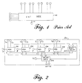
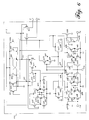
- This invention relates to a self-resetting CMOS (SRCMOS) circuitry and more particularly to SRCMOS circuitry for converting a pulsed input signal to a static output signal for circuitry requiring longer duration signals.
- SRCMOS self-resetting CMOS
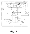
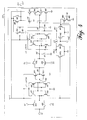
- the circuit 202 is reset by means of a low going pulse on input RS1, which is connected to the gate inputs of p-type gates 203 and 208.
- the low going pulse will cause these gates to conduct to provide a charging current to nodes 215 and 216.
- P-type gates 204 and 207 have their gate inputs connected to ground to provide a low magnitude current to the nodes 215 and 216.
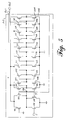
- FIG. 4 is a circuit diagram representation of the driver and latch circuit 210 shown in FIG. 2.
- FIG. 2 shows the inputs C and T which represent the wired-or of the outputs c and t of the MUX circuits 202, 204, 206 and 208.
- the circuit 210 is initially in a standby state as a result of a positive going pulse having been applied to input RS2 connected to gate inputs of n-type gates 401 and 402.
- node 406 When the input signal RS2 goes high, node 406 will be connected to ground through gate 401, causing gate 415 to remain in the conducting state. Furthermore, the reset will also cause the node 405 to be connected to ground, through gate 402. However, this will not effect the state of node 413 since gate 404, which was in the nonconducting state, and gate 409 which was in the conducting state will remain in the conducting state. Hence, the gate input of p-type gate 416 will remain in the conducting state and the output 450 will remain connected to voltage source V through the operation of gates 415 and 416, even though gate 422, which has its gate input connected to node 405, will be turned off.
- the circuit 210 is provided with a test activated circuit input si and a test output sc, as well as clock signals: at, ac, bt, bc, representing true and complement inputs.
- clock signals at, ac, bt, bc, representing true and complement inputs.
- the n-type gate 430 When a clock at is active, and a voltage representing a logical high is applied to the si input, the n-type gate 430 will conduct and the latch L1 will be set such that node 460 will be connected to ground through n-type gate 431. As a consequence, the p-type gate 435 will conduct causing the node 461 to be raised to the high logic level defined by the voltage source V.
- P-type gate 440 and n-type 441 are connected in series between the voltage source V and ground with the sc output terminal connected between the two gates.
- the gate inputs of gates 440 and 441 are directly connected to the node 413.
- gate 440 will conduct and the high value will be provided at test output sc. Therefore, the test output sc will always read the current state of the L2 latch.
- output RS1 Since the output RS1 is connected between gates 515 and 516, the state of this output will change from a high logical level to a low logic level and cause the reset function to be initiated in the MUX circuits 202, 204, 206 and 208. Furthermore, the low level on output on RS1 to the input of p-type gate 517 causes this gate to conduct and provide a high logic level to the input of n-type gate 520 which in turn provides a low input to p-type gate 521 and n-type gate 522. As a result, output RS2 changes from a low logic level to a high logic level signal which initiates the reset action of the driver and latch circuit 210.
- the latch L2 will be reset by the low state of node 655, which is connected to the gate input of p-type gate 631 and the gate input of n-type gate 640, causing the flip-flop to be reset such that node 655 remains low after the disappearance of the RS1 reset pulse. Consequently, node 654 on the other side of latch L2 will be in the high state charging the Ca input gate 639.
Landscapes
- Logic Circuits (AREA)
- Electronic Switches (AREA)
- Tests Of Electronic Circuits (AREA)
Applications Claiming Priority (2)
| Application Number | Priority Date | Filing Date | Title |
|---|---|---|---|
| US309811 | 1994-09-21 | ||
| US08/309,811 US5552745A (en) | 1994-09-21 | 1994-09-21 | Self-resetting CMOS multiplexer with static output driver |
Publications (2)
| Publication Number | Publication Date |
|---|---|
| EP0703668A2 true EP0703668A2 (de) | 1996-03-27 |
| EP0703668A3 EP0703668A3 (de) | 1997-10-15 |
Family
ID=23199758
Family Applications (1)
| Application Number | Title | Priority Date | Filing Date |
|---|---|---|---|
| EP95112832A Withdrawn EP0703668A3 (de) | 1994-09-21 | 1995-08-16 | CMOS-Multiplexeur mit selbsttätiger Rückstellung und statischem Ausgangstreiber |
Country Status (3)
| Country | Link |
|---|---|
| US (2) | US5552745A (de) |
| EP (1) | EP0703668A3 (de) |
| JP (1) | JPH08111632A (de) |
Cited By (4)
| Publication number | Priority date | Publication date | Assignee | Title |
|---|---|---|---|---|
| EP1049257A3 (de) * | 1999-03-09 | 2002-01-02 | Vitesse Semiconductor Corporation | Phasenauswahlschaltung |
| EP1193714A3 (de) * | 2000-10-02 | 2003-05-14 | Broadcom Corporation | Hochschwindigkeitsbankauswahlmultiplexorverriegler |
| US6621312B2 (en) | 2000-11-13 | 2003-09-16 | Primarion, Inc. | High bandwidth multi-phase clock selector with continuous phase output |
| US10713915B2 (en) | 2008-10-24 | 2020-07-14 | Ilumisys, Inc. | Integration of LED lighting control with emergency notification systems |
Families Citing this family (9)
| Publication number | Priority date | Publication date | Assignee | Title |
|---|---|---|---|---|
| US5701447A (en) * | 1995-07-28 | 1997-12-23 | Intel Corporation | Method and apparatus for eliminating latch propagation delays in an alignment unit for use in a fractional bus architecture |
| US5777505A (en) * | 1996-01-25 | 1998-07-07 | The Boeing Company | Low-power crosspoint switch |
| US5815023A (en) * | 1997-03-20 | 1998-09-29 | Sun Microsystems, Inc. | Unbalanced multiplexer and arbiter combination |
| JPH1166890A (ja) * | 1997-08-12 | 1999-03-09 | Mitsubishi Electric Corp | 半導体集積回路装置 |
| US6252445B1 (en) * | 1999-03-31 | 2001-06-26 | Agilent Technologies, Inc. | Method and apparatus for extending a resolution of a clock |
| US6614265B2 (en) * | 2000-05-12 | 2003-09-02 | International Business Machines Corporation | Static logic compatible multiport latch |
| US6674671B1 (en) * | 2002-08-14 | 2004-01-06 | Broadcom Corp. | Circuit for lines with multiple drivers |
| KR100894984B1 (ko) * | 2003-01-20 | 2009-04-24 | 삼성전자주식회사 | 동기형 출력버퍼, 동기형 메모리장치 및 액세스 타임측정방법 |
| KR100714021B1 (ko) | 2006-06-15 | 2007-05-04 | 주식회사 하이닉스반도체 | 출력 신호의 출력 지연 시간을 감소시키는 먹싱 회로 |
Family Cites Families (11)
| Publication number | Priority date | Publication date | Assignee | Title |
|---|---|---|---|---|
| DE3373759D1 (en) * | 1982-06-09 | 1987-10-22 | Fujitsu Ltd | One-chip semiconductor device incorporating a power-supply-potential detecting circuit with reset function |
| JPS61263313A (ja) * | 1985-05-17 | 1986-11-21 | Matsushita Electric Ind Co Ltd | セレクタ付ラツチ回路 |
| US5295174A (en) * | 1990-11-21 | 1994-03-15 | Nippon Steel Corporation | Shifting circuit and shift register |
| US5220213A (en) * | 1991-03-06 | 1993-06-15 | Quicklogic Corporation | Programmable application specific integrated circuit and logic cell therefor |
| US5155380A (en) * | 1991-04-12 | 1992-10-13 | Acer Incorporated | Clock switching circuit and method for preventing glitch during switching |
| US5189319A (en) * | 1991-10-10 | 1993-02-23 | Intel Corporation | Power reducing buffer/latch circuit |
| US5250852A (en) * | 1992-04-16 | 1993-10-05 | Texas Instruments Incorporated | Circuitry and method for latching a logic state |
| US5164612A (en) * | 1992-04-16 | 1992-11-17 | Kaplinsky Cecil H | Programmable CMOS flip-flop emptying multiplexers |
| US5371766A (en) * | 1992-11-20 | 1994-12-06 | International Business Machines Corporation | Clock extraction and data regeneration logic for multiple speed data communications systems |
| US5329529A (en) * | 1993-04-02 | 1994-07-12 | Thomson Consumer Electronics, Inc. | Digital data arbitration apparatus |
| US5410194A (en) * | 1993-08-11 | 1995-04-25 | Xilinx, Inc. | Asynchronous or synchronous load multifunction flip-flop |
-
1994
- 1994-09-21 US US08/309,811 patent/US5552745A/en not_active Expired - Fee Related
-
1995
- 1995-06-02 US US08/459,048 patent/US5568076A/en not_active Expired - Fee Related
- 1995-08-16 EP EP95112832A patent/EP0703668A3/de not_active Withdrawn
- 1995-09-06 JP JP7228725A patent/JPH08111632A/ja active Pending
Non-Patent Citations (1)
| Title |
|---|
| None |
Cited By (5)
| Publication number | Priority date | Publication date | Assignee | Title |
|---|---|---|---|---|
| EP1049257A3 (de) * | 1999-03-09 | 2002-01-02 | Vitesse Semiconductor Corporation | Phasenauswahlschaltung |
| EP1193714A3 (de) * | 2000-10-02 | 2003-05-14 | Broadcom Corporation | Hochschwindigkeitsbankauswahlmultiplexorverriegler |
| US6630856B2 (en) | 2000-10-02 | 2003-10-07 | Broadcom Corporation | High-speed bank select multiplexer latch |
| US6621312B2 (en) | 2000-11-13 | 2003-09-16 | Primarion, Inc. | High bandwidth multi-phase clock selector with continuous phase output |
| US10713915B2 (en) | 2008-10-24 | 2020-07-14 | Ilumisys, Inc. | Integration of LED lighting control with emergency notification systems |
Also Published As
| Publication number | Publication date |
|---|---|
| US5552745A (en) | 1996-09-03 |
| EP0703668A3 (de) | 1997-10-15 |
| US5568076A (en) | 1996-10-22 |
| JPH08111632A (ja) | 1996-04-30 |
Similar Documents
| Publication | Publication Date | Title |
|---|---|---|
| US5488319A (en) | Latch interface for self-reset logic | |
| US5264738A (en) | Flip-flop circuit having transfer gate delay | |
| CA1257344A (en) | Dual domino cmos logic circuit, including complementary vectorization and integration | |
| US5867049A (en) | Zero setup time flip flop | |
| US4806786A (en) | Edge set/reset latch circuit having low device count | |
| US5552745A (en) | Self-resetting CMOS multiplexer with static output driver | |
| EP0476940B1 (de) | Verriegelungsschaltung mit verminderter Metastabilität | |
| US6870408B2 (en) | Power-up circuit | |
| US5892372A (en) | Creating inversions in ripple domino logic | |
| EP0502732B1 (de) | Impulsgenerator | |
| EP0128194B1 (de) | Programmierte logikmatrix | |
| EP0477706B1 (de) | Schaltung zum Synchronisieren von asynchronen Zustandsmaschinen | |
| GB2220272A (en) | Testing digital circuits | |
| JP2853807B2 (ja) | 集積回路 | |
| US5859547A (en) | Dynamic logic circuit | |
| EP0862269A2 (de) | Datenverriegelungs-Schaltungsvorrichtung mit synchronem Halbleiterflipflop-DRAM-Speicher | |
| US5541537A (en) | High speed static circuit design | |
| EP1087529B1 (de) | Halteschaltung in Dominologic mit Rückstellzeit | |
| US6445236B1 (en) | Master-slave flip-flop circuit with embedded hold function and method for holding data in a master-slave flip-flop circuit | |
| US5818264A (en) | Dynamic circuit having improved noise immunity and method therefor | |
| US5638008A (en) | Method and apparatus for generating an asynchronously clocked signal in a synchronously clocked programmable device | |
| US4816702A (en) | CMOS logic circuit | |
| EP0928069A2 (de) | Selbstrücksetzende dynamische logische Schaltungen und Verfahren dazu | |
| US6708261B1 (en) | Multi-stage data buffers having efficient data transfer characteristics and methods of operating same | |
| US5278456A (en) | Process independent digital clock signal shaping network |
Legal Events
| Date | Code | Title | Description |
|---|---|---|---|
| PUAI | Public reference made under article 153(3) epc to a published international application that has entered the european phase |
Free format text: ORIGINAL CODE: 0009012 |
|
| AK | Designated contracting states |
Kind code of ref document: A2 Designated state(s): DE FR GB |
|
| PUAL | Search report despatched |
Free format text: ORIGINAL CODE: 0009013 |
|
| AK | Designated contracting states |
Kind code of ref document: A3 Designated state(s): DE FR GB |
|
| STAA | Information on the status of an ep patent application or granted ep patent |
Free format text: STATUS: THE APPLICATION IS DEEMED TO BE WITHDRAWN |
|
| 18D | Application deemed to be withdrawn |
Effective date: 19980416 |