EP0704068B1 - Composant optique - Google Patents
Composant optique Download PDFInfo
- Publication number
- EP0704068B1 EP0704068B1 EP94916885A EP94916885A EP0704068B1 EP 0704068 B1 EP0704068 B1 EP 0704068B1 EP 94916885 A EP94916885 A EP 94916885A EP 94916885 A EP94916885 A EP 94916885A EP 0704068 B1 EP0704068 B1 EP 0704068B1
- Authority
- EP
- European Patent Office
- Prior art keywords
- layers
- layer
- optical component
- porous silicon
- optical
- Prior art date
- Legal status (The legal status is an assumption and is not a legal conclusion. Google has not performed a legal analysis and makes no representation as to the accuracy of the status listed.)
- Expired - Lifetime
Links
Images


Classifications
-
- H—ELECTRICITY
- H10—SEMICONDUCTOR DEVICES; ELECTRIC SOLID-STATE DEVICES NOT OTHERWISE PROVIDED FOR
- H10H—INORGANIC LIGHT-EMITTING SEMICONDUCTOR DEVICES HAVING POTENTIAL BARRIERS
- H10H20/00—Individual inorganic light-emitting semiconductor devices having potential barriers, e.g. light-emitting diodes [LED]
- H10H20/80—Constructional details
- H10H20/84—Coatings, e.g. passivation layers or antireflective coatings
-
- H—ELECTRICITY
- H10—SEMICONDUCTOR DEVICES; ELECTRIC SOLID-STATE DEVICES NOT OTHERWISE PROVIDED FOR
- H10F—INORGANIC SEMICONDUCTOR DEVICES SENSITIVE TO INFRARED RADIATION, LIGHT, ELECTROMAGNETIC RADIATION OF SHORTER WAVELENGTH OR CORPUSCULAR RADIATION
- H10F30/00—Individual radiation-sensitive semiconductor devices in which radiation controls the flow of current through the devices, e.g. photodetectors
- H10F30/20—Individual radiation-sensitive semiconductor devices in which radiation controls the flow of current through the devices, e.g. photodetectors the devices having potential barriers, e.g. phototransistors
- H10F30/21—Individual radiation-sensitive semiconductor devices in which radiation controls the flow of current through the devices, e.g. photodetectors the devices having potential barriers, e.g. phototransistors the devices being sensitive to infrared, visible or ultraviolet radiation
- H10F30/22—Individual radiation-sensitive semiconductor devices in which radiation controls the flow of current through the devices, e.g. photodetectors the devices having potential barriers, e.g. phototransistors the devices being sensitive to infrared, visible or ultraviolet radiation the devices having only one potential barrier, e.g. photodiodes
- H10F30/221—Individual radiation-sensitive semiconductor devices in which radiation controls the flow of current through the devices, e.g. photodetectors the devices having potential barriers, e.g. phototransistors the devices being sensitive to infrared, visible or ultraviolet radiation the devices having only one potential barrier, e.g. photodiodes the potential barrier being a PN homojunction
-
- H—ELECTRICITY
- H10—SEMICONDUCTOR DEVICES; ELECTRIC SOLID-STATE DEVICES NOT OTHERWISE PROVIDED FOR
- H10F—INORGANIC SEMICONDUCTOR DEVICES SENSITIVE TO INFRARED RADIATION, LIGHT, ELECTROMAGNETIC RADIATION OF SHORTER WAVELENGTH OR CORPUSCULAR RADIATION
- H10F77/00—Constructional details of devices covered by this subclass
- H10F77/30—Coatings
- H10F77/306—Coatings for devices having potential barriers
- H10F77/331—Coatings for devices having potential barriers for filtering or shielding light, e.g. multicolour filters for photodetectors
- H10F77/337—Coatings for devices having potential barriers for filtering or shielding light, e.g. multicolour filters for photodetectors using interference filters, e.g. multilayer dielectric filters
-
- H—ELECTRICITY
- H10—SEMICONDUCTOR DEVICES; ELECTRIC SOLID-STATE DEVICES NOT OTHERWISE PROVIDED FOR
- H10H—INORGANIC LIGHT-EMITTING SEMICONDUCTOR DEVICES HAVING POTENTIAL BARRIERS
- H10H20/00—Individual inorganic light-emitting semiconductor devices having potential barriers, e.g. light-emitting diodes [LED]
- H10H20/80—Constructional details
- H10H20/81—Bodies
- H10H20/822—Materials of the light-emitting regions
- H10H20/826—Materials of the light-emitting regions comprising only Group IV materials
- H10H20/8264—Materials of the light-emitting regions comprising only Group IV materials comprising polycrystalline, amorphous or porous Group IV materials
-
- H—ELECTRICITY
- H01—ELECTRIC ELEMENTS
- H01S—DEVICES USING THE PROCESS OF LIGHT AMPLIFICATION BY STIMULATED EMISSION OF RADIATION [LASER] TO AMPLIFY OR GENERATE LIGHT; DEVICES USING STIMULATED EMISSION OF ELECTROMAGNETIC RADIATION IN WAVE RANGES OTHER THAN OPTICAL
- H01S5/00—Semiconductor lasers
- H01S5/10—Construction or shape of the optical resonator, e.g. extended or external cavity, coupled cavities, bent-guide, varying width, thickness or composition of the active region
- H01S5/18—Surface-emitting [SE] lasers, e.g. having both horizontal and vertical cavities
- H01S5/183—Surface-emitting [SE] lasers, e.g. having both horizontal and vertical cavities having only vertical cavities, e.g. vertical cavity surface-emitting lasers [VCSEL]
-
- H—ELECTRICITY
- H01—ELECTRIC ELEMENTS
- H01S—DEVICES USING THE PROCESS OF LIGHT AMPLIFICATION BY STIMULATED EMISSION OF RADIATION [LASER] TO AMPLIFY OR GENERATE LIGHT; DEVICES USING STIMULATED EMISSION OF ELECTROMAGNETIC RADIATION IN WAVE RANGES OTHER THAN OPTICAL
- H01S5/00—Semiconductor lasers
- H01S5/30—Structure or shape of the active region; Materials used for the active region
- H01S5/32—Structure or shape of the active region; Materials used for the active region comprising PN junctions, e.g. hetero- or double- heterostructures
- H01S5/3223—IV compounds
- H01S5/3224—Si
- H01S5/3227—Si porous Si
Definitions
- the invention relates to an optical component, consisting of transparent, thin layers different thickness and different refractive indices.
- optical components have long been known.
- optical components used their effect on interference effects in based on thin layers.
- This is for example Uni interference filter and mirror.
- the desired Effect of a sequence of layers that generally out Layers with two materials that are different Have refractive index, is made by a suitable choice of the layer sequence and the optical Thickness of the individual layers determined.
- the so-called optical Thickness is the thickness of the layer multiplied by the refractive index.
- These are optical layer thicknesses usually whole fractions of that wavelength, for which the filter or mirror is designed.
- a so-called Bragg reflector consists of a periodic one Layer sequence of two layers with as different as possible Refractive index and an optical layer thickness of 1/4 of the wavelength for which the reflector should have optimal effect.
- Fabry-Perot filter which is a bit modified layer sequence, one for one certain wavelength defined high transmission, while for other wavelengths the filter is opaque is.
- Optical components from layers with gradually changed Refractive index are as waveguides or as Antireflection coatings known.
- the layers consist of porous silicon.
- the methods mentioned under a) to d) can be also combine with each other, so the optical properties to optimally design the layer system.
- the layer system according to the invention can, depending on the desired Use case can be varied and so Emission or absorption characteristics of a light emitting Component or photodetector (filter, Anti-reflective coating) can be influenced. So there is a version of the optical component in that the Layers of thicknesses and refractive indices in the manner of a Have interference filters and can be used as such are.
- the filter effect is a periodic sequence of layers with different optical properties (dielectric functions) achieved.
- different types of filters can be implemented (Bandpass, bandstop, Fabry Perot filter)
- the Filter effect also through the series connection of different types of filters can be combined.
- Such Filters are both in optics and for influencing the emission characteristics of light emitting Components (e.g. colored flat screen also made of porous silicon) and as a front filter for photodiodes, e.g. usable with color cameras.
- porous silicon as Layer material are not only in the light and cheap manufacturability of any complex Layer systems, but also in the possibility of gradual To achieve transitions in the refractive index.
- compositions have a continuously changing refractive index and therefore retlex-reducing or reflex-enhancing Have an effect.
- the gradual transitions in the refractive index are included necessary for optimal shaft guidance in one To achieve optical fibers, as is the case with glass fibers Case is. Due to the possibility, also in layer system gradual transitions in the refractive index from porous silicon are waveguides on one Silicon chip can be produced in a very simple manner. At A waveguide should have the layer sequence of porous Silicon a gradually increasing and decreasing Have refractive index. In addition to the filter effect of layer systems can thus be gradual Change in the optical properties of a layer system made of porous silicon an anti-reflective / anti-reflective Top layer can be produced. This is both to reduce internal reflections decoupling in the case of light emitters Structures like waveguides as well as reduction the reflectivity in photodetectors or as Anti-reflective coating, e.g. for solar cells, applicable.
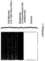
- the figure shows a structure that looks like this composed:
- the main one is located directly on the substrate Part of the component, which is either light detected or emitted.
- a layer system which is used as a filter works.
- layers of different porosity too have different sized refractive indices.
- This layer system can e.g. a Fabry-Perot Be a filter.
- the entire structure is etched electrochemically produced from a silicon wafer.
- the layer systems made of porous silicon can be apply very differently. There are two uses shown here:
- a layer system can be manufactured so that it is transparent to the wavelength of color 1, while it a highly reflective for the wavelength of color 2 Represents mirror. Will this structure Made on a wafer, you get a reflection filter for a certain wavelength. All other wavelengths are absorbed in the device. This type of application is on the left shown in the figure.
- the filter is made self-supporting. In this way a splinter of paint is produced, which reflects a certain wavelength and lets the others through. This structure is on the right Page shown in the drawing.
- a light guide on a chip can also directly from the silicon wafer of the chip getting produced.
- Layer system produced which a course in Refractive index as it is on the left the drawing is shown.
- the light-guiding layer lies in the middle of the layer system and has the largest refractive index. The light is coupled in from the side edge of the layer system.
Landscapes
- Optical Filters (AREA)
- Optical Integrated Circuits (AREA)
- Optical Elements Other Than Lenses (AREA)
- Surface Treatment Of Optical Elements (AREA)
- Led Devices (AREA)
Abstract
Claims (4)
- Composant optique, constitué de minces couches transparentes d'épaisseurs différentes et d'indices de réfraction différents, caractérisé en ce que les couches sont en silicium poreux.
- Composant optique suivant la revendication 1, caractérisé en ce que les couches ont des épaisseurs et un indice de réfraction du genre d'un filtre à interférence ou d'un miroir à interférence et peuvent être utilisées comme telles.
- Composant optique suivant la revendication 1, caractérisé on ce que les couches ont un indice de réfraction qui varie de manière continue.
- Composant optique suivant la revendication 3, caractérisé en ce que la succession de couches a un indice de réfraction qui augmente graduellement et diminue à nouveau.
Applications Claiming Priority (3)
| Application Number | Priority Date | Filing Date | Title |
|---|---|---|---|
| DE4319413 | 1993-06-14 | ||
| DE4319413A DE4319413C2 (de) | 1993-06-14 | 1993-06-14 | Interferenzfilter oder dielektrischer Spiegel |
| PCT/DE1994/000635 WO1994029757A1 (fr) | 1993-06-14 | 1994-06-08 | Composant optique |
Publications (2)
| Publication Number | Publication Date |
|---|---|
| EP0704068A1 EP0704068A1 (fr) | 1996-04-03 |
| EP0704068B1 true EP0704068B1 (fr) | 2000-09-13 |
Family
ID=6490150
Family Applications (1)
| Application Number | Title | Priority Date | Filing Date |
|---|---|---|---|
| EP94916885A Expired - Lifetime EP0704068B1 (fr) | 1993-06-14 | 1994-06-08 | Composant optique |
Country Status (5)
| Country | Link |
|---|---|
| US (1) | US5696629A (fr) |
| EP (1) | EP0704068B1 (fr) |
| JP (1) | JP3615760B2 (fr) |
| DE (2) | DE4319413C2 (fr) |
| WO (1) | WO1994029757A1 (fr) |
Families Citing this family (36)
| Publication number | Priority date | Publication date | Assignee | Title |
|---|---|---|---|---|
| US5828118A (en) * | 1993-09-09 | 1998-10-27 | The United States Of America As Represented By The Secretary Of The Navy | System which uses porous silicon for down converting electromagnetic energy to an energy level within the bandpass of an electromagnetic energy detector |
| US5699188A (en) * | 1995-06-26 | 1997-12-16 | Minnesota Mining And Manufacturing Co. | Metal-coated multilayer mirror |
| DE19609073A1 (de) * | 1996-03-08 | 1997-09-11 | Forschungszentrum Juelich Gmbh | Farbselektives Si-Detektorarray |
| GB2312090A (en) * | 1996-04-10 | 1997-10-15 | Rank Taylor Hobson Ltd | Photosensitive device |
| DE19622748A1 (de) * | 1996-06-05 | 1997-12-11 | Forschungszentrum Juelich Gmbh | Interferenzfilter auf der Basis von porösem Silicium |
| DE19638885C1 (de) * | 1996-09-21 | 1998-04-23 | Forschungszentrum Juelich Gmbh | Optisches Beugungsgitter auf der Basis eines porösen Materials |
| DE19653097A1 (de) | 1996-12-20 | 1998-07-02 | Forschungszentrum Juelich Gmbh | Schicht mit porösem Schichtbereich, eine solche Schicht enthaltendes Interferenzfilter sowie Verfahren zu ihrer Herstellung |
| FR2758003B1 (fr) * | 1996-12-27 | 1999-06-18 | France Telecom | Traitement anti-reflet de surfaces reflectives |
| DE19738607B4 (de) * | 1997-09-04 | 2008-07-31 | Robert Bosch Gmbh | Mikrospiegel und Verfahren zur Herstellung eines Mikrospiegels |
| US6037612A (en) | 1997-09-11 | 2000-03-14 | Kokusai Denshin Denwa Kabushiki Kaisha | Semiconductor light emitting device having nanostructure porous silicon and mesostructure porous silicon |
| DE19740096A1 (de) * | 1997-09-12 | 1999-03-25 | Forschungszentrum Juelich Gmbh | Verfahren zur Herstellung einer oder mehrerer optischer Komponenten in porösem Silicium sowie solche optische Komponenten enthaltenes Bauelement |
| DE19746089A1 (de) * | 1997-10-20 | 1999-04-29 | Forschungszentrum Juelich Gmbh | Eine Filterstruktur aufweisendes Bauelement |
| DE19757560A1 (de) * | 1997-12-23 | 1999-07-01 | Forschungszentrum Juelich Gmbh | Verfahren zur Herstellung einer porösen Schicht mit Hilfe eines elektrochemischen Ätzprozesses |
| EP0969522A1 (fr) * | 1998-07-03 | 2000-01-05 | Interuniversitair Microelektronica Centrum Vzw | Dispositif optoélectronique à couche mince et son procédé de fabrication |
| AU4593499A (en) | 1998-07-03 | 2000-01-24 | Interuniversitair Micro-Elektronica Centrum | A thin-film opto-electronic device and a method of making it |
| DE19900879A1 (de) | 1999-01-12 | 2000-08-17 | Forschungszentrum Juelich Gmbh | Optischer Detektor mit einer Filterschicht aus porösem Silizium und Herstellungsverfahren dazu |
| US6370307B1 (en) * | 1999-07-15 | 2002-04-09 | Agere Systems Guardian Corp. | Optical device formed on a substrate with thermal isolation regions formed therein |
| FR2797093B1 (fr) * | 1999-07-26 | 2001-11-02 | France Telecom | Procede de realisation d'un dispositif comprenant un empilement de plans de boites quantiques sur un substrat de silicium ou germanium monocristallin |
| EP1088785A1 (fr) * | 1999-09-10 | 2001-04-04 | Ecole Polytechnique Federale De Lausanne | Procédé de fabrication d'une microstructure intégrée suspendue tridimensionnelle, microstructure intégrée notamment obtenue par ce procédé et élément optique intégré réglable |
| DE10160987B4 (de) * | 2001-12-05 | 2005-08-04 | Siemens Ag | Baueinheit zur simultanen, optischen Beleuchtung einer Vielzahl von Proben |
| US8765484B2 (en) * | 2002-02-07 | 2014-07-01 | The Regents Of The University Of California | Optically encoded particles |
| US7022544B2 (en) * | 2002-12-18 | 2006-04-04 | International Business Machines Corporation | High speed photodiode with a barrier layer for blocking or eliminating slow photonic carriers and method for forming same |
| AU2004308380A1 (en) * | 2003-12-22 | 2005-07-14 | The Regents Of The University Of California | Optically encoded particles, system and high-throughput screening |
| US7560018B2 (en) | 2004-01-21 | 2009-07-14 | Lake Shore Cryotronics, Inc. | Semiconductor electrochemical etching processes employing closed loop control |
| US20060027459A1 (en) * | 2004-05-28 | 2006-02-09 | Lake Shore Cryotronics, Inc. | Mesoporous silicon infrared filters and methods of making same |
| US7994600B2 (en) * | 2005-12-21 | 2011-08-09 | Texas Instruments Incorporated | Antireflective coating |
| JP5526331B2 (ja) | 2007-04-27 | 2014-06-18 | 国立大学法人 香川大学 | 反射防止膜およびその製造方法。 |
| US20090110356A1 (en) * | 2007-06-18 | 2009-04-30 | Xiao-Dong Xiang | Methods and apparatuses for waveguiding luminescence generated in a scattering medium |
| US7808657B2 (en) * | 2007-06-28 | 2010-10-05 | International Business Machines Corporation | Wafer and stage alignment using photonic devices |
| JP2011505267A (ja) * | 2007-11-08 | 2011-02-24 | エム. セイガー、ブライアン | 改善された反射防止用被覆 |
| US8080849B2 (en) * | 2008-01-17 | 2011-12-20 | International Business Machines Corporation | Characterizing films using optical filter pseudo substrate |
| US20090316250A1 (en) * | 2008-06-18 | 2009-12-24 | Lee Boman | Window having wavelength selectivity and photovoltaic capability |
| WO2012103292A1 (fr) * | 2011-01-26 | 2012-08-02 | Massachusetts Institute Of Technology | Dispositif et procédé d'augmentation de la luminescence par transfert d'énergie par résonance depuis une couche mince absorbante |
| MX351488B (es) * | 2013-05-17 | 2017-06-30 | Univ Autonoma Del Estado De Morelos | Estructura antirreflejante cuasi-omnidireccional basada en multicapas dieléctricas de silicio poroso para la región ultravioleta media, visible e infrarroja cercana al espectro electromagnético. |
| CN103779636B (zh) * | 2014-01-10 | 2015-10-28 | 上海理工大学 | 基于多孔硅的太赫兹滤波器 |
| CN105842785A (zh) * | 2016-05-20 | 2016-08-10 | 燕山大学 | 基于啁啾多孔硅光子晶体的多通道滤波器 |
Family Cites Families (5)
| Publication number | Priority date | Publication date | Assignee | Title |
|---|---|---|---|---|
| US4271210A (en) * | 1979-10-25 | 1981-06-02 | Westinghouse Electric Corp. | Method of forming transmissive, porous metal oxide optical layer of a vitreous substrate |
| US4535026A (en) * | 1983-06-29 | 1985-08-13 | The United States Of America As Represented By The United States Department Of Energy | Antireflective graded index silica coating, method for making |
| US4633131A (en) * | 1984-12-12 | 1986-12-30 | North American Philips Corporation | Halo-reducing faceplate arrangement |
| JPS61170702A (ja) * | 1985-01-25 | 1986-08-01 | Kunio Yoshida | 光学薄膜の製作方法 |
| US5218472A (en) * | 1989-03-22 | 1993-06-08 | Alcan International Limited | Optical interference structures incorporating porous films |
-
1993
- 1993-06-14 DE DE4319413A patent/DE4319413C2/de not_active Expired - Lifetime
-
1994
- 1994-06-08 US US08/564,335 patent/US5696629A/en not_active Expired - Lifetime
- 1994-06-08 EP EP94916885A patent/EP0704068B1/fr not_active Expired - Lifetime
- 1994-06-08 WO PCT/DE1994/000635 patent/WO1994029757A1/fr not_active Ceased
- 1994-06-08 DE DE59409521T patent/DE59409521D1/de not_active Expired - Lifetime
- 1994-06-08 JP JP50118595A patent/JP3615760B2/ja not_active Expired - Lifetime
Also Published As
| Publication number | Publication date |
|---|---|
| WO1994029757A1 (fr) | 1994-12-22 |
| EP0704068A1 (fr) | 1996-04-03 |
| DE4319413A1 (de) | 1994-12-15 |
| DE59409521D1 (de) | 2000-10-19 |
| US5696629A (en) | 1997-12-09 |
| JP3615760B2 (ja) | 2005-02-02 |
| JPH10508113A (ja) | 1998-08-04 |
| DE4319413C2 (de) | 1999-06-10 |
Similar Documents
| Publication | Publication Date | Title |
|---|---|---|
| EP0704068B1 (fr) | Composant optique | |
| DE68918764T2 (de) | Wellenlängenmultiplexermodul. | |
| EP1293018B1 (fr) | Laser a fibre optique | |
| DE69404701T2 (de) | Abstimmbarer oberflächenemittierender Halbleiterlaser | |
| EP0985159B1 (fr) | Circuit optique integre | |
| DE3873689T2 (de) | Halbleiterlaser. | |
| DE3903019A1 (de) | Optische farbteiler-anordnung | |
| DE3920416A1 (de) | Optisches bauteil, und verfahren zu seiner herstellung | |
| EP2702364A1 (fr) | Dispositif pour mesurer des paramètres d'état | |
| EP0053324A2 (fr) | Diviseur optique | |
| EP0212438A2 (fr) | Réseau de diffraction à réflexion ayant un haut coefficient de réflexion | |
| DE102007033567A1 (de) | Phasenschiebe-Einrichtung und Laserresonator zur Erzeugung radial oder azimutal polarisierter Laserstrahlung | |
| EP2478400A2 (fr) | Filtres de modes transversaux pour guide d'onde | |
| DE68903311T2 (de) | Optische sensorsysteme. | |
| EP1560306A2 (fr) | VCSEL avec filtre optique | |
| EP0831343A2 (fr) | Guide d'ondes optique et son procédé de fabrication | |
| DE3329719A1 (de) | Fotodiode mit resonatorstruktur zur absorptionserhoehung | |
| DE69109433T2 (de) | Wellenlängenfilter in Form eines optischen Wellenleiters. | |
| DE4120198A1 (de) | Integriert optische schaltung | |
| DE102020112806A1 (de) | Halbleiterlaserbauelement und verfahren zum betrieb zumindest eines halbleiterlasers | |
| DE102015222328A1 (de) | Optische Komponente und Verfahren zu deren Herstellung | |
| EP0923798A1 (fr) | Laser a guide d'ondes multimode pompe par diode laser en particulier un laser a fibre | |
| DE10227367B4 (de) | Reflektierendes Element für freie Elektronen-Laserstrahlung, Verfahren zu seiner Herstellung und seine Verwendung | |
| EP0173930A2 (fr) | Multiplexeur/démultiplexeur optique | |
| DE69901194T2 (de) | Bragg-Gitter für optische Faser mit verschobener äquivalenter Spiegelebene und Herstellungsmethode dafür |
Legal Events
| Date | Code | Title | Description |
|---|---|---|---|
| PUAI | Public reference made under article 153(3) epc to a published international application that has entered the european phase |
Free format text: ORIGINAL CODE: 0009012 |
|
| 17P | Request for examination filed |
Effective date: 19951208 |
|
| AK | Designated contracting states |
Kind code of ref document: A1 Designated state(s): DE FR GB IT NL |
|
| 17Q | First examination report despatched |
Effective date: 19960705 |
|
| GRAG | Despatch of communication of intention to grant |
Free format text: ORIGINAL CODE: EPIDOS AGRA |
|
| GRAG | Despatch of communication of intention to grant |
Free format text: ORIGINAL CODE: EPIDOS AGRA |
|
| GRAH | Despatch of communication of intention to grant a patent |
Free format text: ORIGINAL CODE: EPIDOS IGRA |
|
| GRAH | Despatch of communication of intention to grant a patent |
Free format text: ORIGINAL CODE: EPIDOS IGRA |
|
| GRAA | (expected) grant |
Free format text: ORIGINAL CODE: 0009210 |
|
| AK | Designated contracting states |
Kind code of ref document: B1 Designated state(s): DE FR GB IT NL |
|
| REF | Corresponds to: |
Ref document number: 59409521 Country of ref document: DE Date of ref document: 20001019 |
|
| ITF | It: translation for a ep patent filed | ||
| ET | Fr: translation filed | ||
| GBT | Gb: translation of ep patent filed (gb section 77(6)(a)/1977) |
Effective date: 20001130 |
|
| PLBE | No opposition filed within time limit |
Free format text: ORIGINAL CODE: 0009261 |
|
| STAA | Information on the status of an ep patent application or granted ep patent |
Free format text: STATUS: NO OPPOSITION FILED WITHIN TIME LIMIT |
|
| 26N | No opposition filed | ||
| REG | Reference to a national code |
Ref country code: GB Ref legal event code: IF02 |
|
| PGFP | Annual fee paid to national office [announced via postgrant information from national office to epo] |
Ref country code: GB Payment date: 20130620 Year of fee payment: 20 Ref country code: DE Payment date: 20130504 Year of fee payment: 20 |
|
| PGFP | Annual fee paid to national office [announced via postgrant information from national office to epo] |
Ref country code: NL Payment date: 20130620 Year of fee payment: 20 Ref country code: FR Payment date: 20130703 Year of fee payment: 20 |
|
| PGFP | Annual fee paid to national office [announced via postgrant information from national office to epo] |
Ref country code: IT Payment date: 20130621 Year of fee payment: 20 |
|
| REG | Reference to a national code |
Ref country code: DE Ref legal event code: R071 Ref document number: 59409521 Country of ref document: DE |
|
| REG | Reference to a national code |
Ref country code: NL Ref legal event code: V4 Effective date: 20140608 |
|
| REG | Reference to a national code |
Ref country code: GB Ref legal event code: PE20 Expiry date: 20140607 |
|
| PG25 | Lapsed in a contracting state [announced via postgrant information from national office to epo] |
Ref country code: GB Free format text: LAPSE BECAUSE OF EXPIRATION OF PROTECTION Effective date: 20140607 |
|
| PG25 | Lapsed in a contracting state [announced via postgrant information from national office to epo] |
Ref country code: DE Free format text: LAPSE BECAUSE OF EXPIRATION OF PROTECTION Effective date: 20140611 |