EP0704742A2 - Optische Steuervorrichtung und Verfahren zu ihrer Herstellung - Google Patents
Optische Steuervorrichtung und Verfahren zu ihrer Herstellung Download PDFInfo
- Publication number
- EP0704742A2 EP0704742A2 EP95306831A EP95306831A EP0704742A2 EP 0704742 A2 EP0704742 A2 EP 0704742A2 EP 95306831 A EP95306831 A EP 95306831A EP 95306831 A EP95306831 A EP 95306831A EP 0704742 A2 EP0704742 A2 EP 0704742A2
- Authority
- EP
- European Patent Office
- Prior art keywords
- crystalline substrate
- control device
- layer
- channel
- film layer
- Prior art date
- Legal status (The legal status is an assumption and is not a legal conclusion. Google has not performed a legal analysis and makes no representation as to the accuracy of the status listed.)
- Withdrawn
Links
- 230000003287 optical effect Effects 0.000 title claims abstract description 178
- 238000000034 method Methods 0.000 title claims description 39
- 239000000758 substrate Substances 0.000 claims abstract description 104
- 229910052751 metal Inorganic materials 0.000 claims abstract description 55
- 239000002184 metal Substances 0.000 claims abstract description 55
- 229910003327 LiNbO3 Inorganic materials 0.000 claims abstract description 39
- 229910012463 LiTaO3 Inorganic materials 0.000 claims abstract description 16
- 230000000694 effects Effects 0.000 claims abstract description 13
- WHXSMMKQMYFTQS-UHFFFAOYSA-N Lithium Chemical compound [Li] WHXSMMKQMYFTQS-UHFFFAOYSA-N 0.000 claims description 94
- 229910052744 lithium Inorganic materials 0.000 claims description 94
- 230000000903 blocking effect Effects 0.000 claims description 70
- 229910052719 titanium Inorganic materials 0.000 claims description 16
- 239000010936 titanium Substances 0.000 claims description 16
- 238000009792 diffusion process Methods 0.000 claims description 15
- 239000000463 material Substances 0.000 claims description 15
- RTAQQCXQSZGOHL-UHFFFAOYSA-N Titanium Chemical compound [Ti] RTAQQCXQSZGOHL-UHFFFAOYSA-N 0.000 claims description 10
- 229910052802 copper Inorganic materials 0.000 claims description 9
- 239000010949 copper Substances 0.000 claims description 9
- 229910052750 molybdenum Inorganic materials 0.000 claims description 9
- 229910052804 chromium Inorganic materials 0.000 claims description 8
- 239000011651 chromium Substances 0.000 claims description 8
- 229910052742 iron Inorganic materials 0.000 claims description 7
- 229910052720 vanadium Inorganic materials 0.000 claims description 7
- 230000015572 biosynthetic process Effects 0.000 claims description 4
- 230000005684 electric field Effects 0.000 claims description 4
- 239000004065 semiconductor Substances 0.000 claims description 4
- 230000010287 polarization Effects 0.000 claims description 3
- VYZAMTAEIAYCRO-UHFFFAOYSA-N Chromium Chemical compound [Cr] VYZAMTAEIAYCRO-UHFFFAOYSA-N 0.000 claims description 2
- 230000005012 migration Effects 0.000 claims description 2
- 238000013508 migration Methods 0.000 claims description 2
- 239000011368 organic material Substances 0.000 claims description 2
- 229910052710 silicon Inorganic materials 0.000 claims description 2
- XEEYBQQBJWHFJM-UHFFFAOYSA-N Iron Chemical compound [Fe] XEEYBQQBJWHFJM-UHFFFAOYSA-N 0.000 claims 3
- RYGMFSIKBFXOCR-UHFFFAOYSA-N Copper Chemical compound [Cu] RYGMFSIKBFXOCR-UHFFFAOYSA-N 0.000 claims 1
- ZOKXTWBITQBERF-UHFFFAOYSA-N Molybdenum Chemical compound [Mo] ZOKXTWBITQBERF-UHFFFAOYSA-N 0.000 claims 1
- 239000011733 molybdenum Substances 0.000 claims 1
- LEONUFNNVUYDNQ-UHFFFAOYSA-N vanadium atom Chemical compound [V] LEONUFNNVUYDNQ-UHFFFAOYSA-N 0.000 claims 1
- VYPSYNLAJGMNEJ-UHFFFAOYSA-N Silicium dioxide Chemical compound O=[Si]=O VYPSYNLAJGMNEJ-UHFFFAOYSA-N 0.000 description 34
- 229910052681 coesite Inorganic materials 0.000 description 17
- 229910052906 cristobalite Inorganic materials 0.000 description 17
- 239000000377 silicon dioxide Substances 0.000 description 17
- 235000012239 silicon dioxide Nutrition 0.000 description 17
- 229910052682 stishovite Inorganic materials 0.000 description 17
- 229910052905 tridymite Inorganic materials 0.000 description 17
- 238000004544 sputter deposition Methods 0.000 description 16
- 238000007740 vapor deposition Methods 0.000 description 12
- 239000000203 mixture Substances 0.000 description 10
- 230000008569 process Effects 0.000 description 10
- 238000005229 chemical vapour deposition Methods 0.000 description 8
- 238000000151 deposition Methods 0.000 description 8
- 150000002500 ions Chemical class 0.000 description 4
- 230000001902 propagating effect Effects 0.000 description 4
- 229910052581 Si3N4 Inorganic materials 0.000 description 3
- 229910008812 WSi Inorganic materials 0.000 description 3
- 230000008901 benefit Effects 0.000 description 3
- 238000005530 etching Methods 0.000 description 3
- 239000010931 gold Substances 0.000 description 3
- 229910052737 gold Inorganic materials 0.000 description 3
- 239000012535 impurity Substances 0.000 description 3
- 238000005468 ion implantation Methods 0.000 description 3
- 238000001459 lithography Methods 0.000 description 3
- 229910001635 magnesium fluoride Inorganic materials 0.000 description 3
- 239000011159 matrix material Substances 0.000 description 3
- 238000000206 photolithography Methods 0.000 description 3
- -1 ITO Inorganic materials 0.000 description 2
- 229910052782 aluminium Inorganic materials 0.000 description 2
- PNEYBMLMFCGWSK-UHFFFAOYSA-N aluminium oxide Inorganic materials [O-2].[O-2].[O-2].[Al+3].[Al+3] PNEYBMLMFCGWSK-UHFFFAOYSA-N 0.000 description 2
- WPYMKLBDIGXBTP-UHFFFAOYSA-N benzoic acid Chemical compound OC(=O)C1=CC=CC=C1 WPYMKLBDIGXBTP-UHFFFAOYSA-N 0.000 description 2
- 230000005540 biological transmission Effects 0.000 description 2
- 238000004891 communication Methods 0.000 description 2
- 229920001940 conductive polymer Polymers 0.000 description 2
- 239000004020 conductor Substances 0.000 description 2
- 229910052593 corundum Inorganic materials 0.000 description 2
- 238000010894 electron beam technology Methods 0.000 description 2
- 230000010354 integration Effects 0.000 description 2
- 238000000059 patterning Methods 0.000 description 2
- 229910052814 silicon oxide Inorganic materials 0.000 description 2
- 229910001845 yogo sapphire Inorganic materials 0.000 description 2
- 239000005711 Benzoic acid Substances 0.000 description 1
- 229910001218 Gallium arsenide Inorganic materials 0.000 description 1
- DGAQECJNVWCQMB-PUAWFVPOSA-M Ilexoside XXIX Chemical compound C[C@@H]1CC[C@@]2(CC[C@@]3(C(=CC[C@H]4[C@]3(CC[C@@H]5[C@@]4(CC[C@@H](C5(C)C)OS(=O)(=O)[O-])C)C)[C@@H]2[C@]1(C)O)C)C(=O)O[C@H]6[C@@H]([C@H]([C@@H]([C@H](O6)CO)O)O)O.[Na+] DGAQECJNVWCQMB-PUAWFVPOSA-M 0.000 description 1
- OAICVXFJPJFONN-UHFFFAOYSA-N Phosphorus Chemical compound [P] OAICVXFJPJFONN-UHFFFAOYSA-N 0.000 description 1
- 239000004642 Polyimide Substances 0.000 description 1
- ZLMJMSJWJFRBEC-UHFFFAOYSA-N Potassium Chemical compound [K] ZLMJMSJWJFRBEC-UHFFFAOYSA-N 0.000 description 1
- 238000010521 absorption reaction Methods 0.000 description 1
- 235000010233 benzoic acid Nutrition 0.000 description 1
- 230000008033 biological extinction Effects 0.000 description 1
- 238000010276 construction Methods 0.000 description 1
- 239000013078 crystal Substances 0.000 description 1
- 230000008021 deposition Effects 0.000 description 1
- XPPKVPWEQAFLFU-UHFFFAOYSA-N diphosphoric acid Chemical compound OP(O)(=O)OP(O)(O)=O XPPKVPWEQAFLFU-UHFFFAOYSA-N 0.000 description 1
- 239000000835 fiber Substances 0.000 description 1
- 238000001914 filtration Methods 0.000 description 1
- PCHJSUWPFVWCPO-UHFFFAOYSA-N gold Chemical compound [Au] PCHJSUWPFVWCPO-UHFFFAOYSA-N 0.000 description 1
- 230000031700 light absorption Effects 0.000 description 1
- GQYHUHYESMUTHG-UHFFFAOYSA-N lithium niobate Chemical compound [Li+].[O-][Nb](=O)=O GQYHUHYESMUTHG-UHFFFAOYSA-N 0.000 description 1
- 230000004048 modification Effects 0.000 description 1
- 238000012986 modification Methods 0.000 description 1
- 239000011574 phosphorus Substances 0.000 description 1
- 229910052698 phosphorus Inorganic materials 0.000 description 1
- 229920001721 polyimide Polymers 0.000 description 1
- 229910052700 potassium Inorganic materials 0.000 description 1
- 239000011591 potassium Substances 0.000 description 1
- 238000012545 processing Methods 0.000 description 1
- 229940005657 pyrophosphoric acid Drugs 0.000 description 1
- 230000009467 reduction Effects 0.000 description 1
- 229910052708 sodium Inorganic materials 0.000 description 1
- 239000011734 sodium Substances 0.000 description 1
- 238000002207 thermal evaporation Methods 0.000 description 1
- 230000008719 thickening Effects 0.000 description 1
Images






Classifications
-
- G—PHYSICS
- G02—OPTICS
- G02F—OPTICAL DEVICES OR ARRANGEMENTS FOR THE CONTROL OF LIGHT BY MODIFICATION OF THE OPTICAL PROPERTIES OF THE MEDIA OF THE ELEMENTS INVOLVED THEREIN; NON-LINEAR OPTICS; FREQUENCY-CHANGING OF LIGHT; OPTICAL LOGIC ELEMENTS; OPTICAL ANALOGUE/DIGITAL CONVERTERS
- G02F1/00—Devices or arrangements for the control of the intensity, colour, phase, polarisation or direction of light arriving from an independent light source, e.g. switching, gating or modulating; Non-linear optics
- G02F1/01—Devices or arrangements for the control of the intensity, colour, phase, polarisation or direction of light arriving from an independent light source, e.g. switching, gating or modulating; Non-linear optics for the control of the intensity, phase, polarisation or colour
- G02F1/03—Devices or arrangements for the control of the intensity, colour, phase, polarisation or direction of light arriving from an independent light source, e.g. switching, gating or modulating; Non-linear optics for the control of the intensity, phase, polarisation or colour based on ceramics or electro-optical crystals, e.g. exhibiting Pockels effect or Kerr effect
- G02F1/035—Devices or arrangements for the control of the intensity, colour, phase, polarisation or direction of light arriving from an independent light source, e.g. switching, gating or modulating; Non-linear optics for the control of the intensity, phase, polarisation or colour based on ceramics or electro-optical crystals, e.g. exhibiting Pockels effect or Kerr effect in an optical waveguide structure
-
- G—PHYSICS
- G02—OPTICS
- G02F—OPTICAL DEVICES OR ARRANGEMENTS FOR THE CONTROL OF LIGHT BY MODIFICATION OF THE OPTICAL PROPERTIES OF THE MEDIA OF THE ELEMENTS INVOLVED THEREIN; NON-LINEAR OPTICS; FREQUENCY-CHANGING OF LIGHT; OPTICAL LOGIC ELEMENTS; OPTICAL ANALOGUE/DIGITAL CONVERTERS
- G02F1/00—Devices or arrangements for the control of the intensity, colour, phase, polarisation or direction of light arriving from an independent light source, e.g. switching, gating or modulating; Non-linear optics
- G02F1/01—Devices or arrangements for the control of the intensity, colour, phase, polarisation or direction of light arriving from an independent light source, e.g. switching, gating or modulating; Non-linear optics for the control of the intensity, phase, polarisation or colour
- G02F1/21—Devices or arrangements for the control of the intensity, colour, phase, polarisation or direction of light arriving from an independent light source, e.g. switching, gating or modulating; Non-linear optics for the control of the intensity, phase, polarisation or colour by interference
- G02F1/225—Devices or arrangements for the control of the intensity, colour, phase, polarisation or direction of light arriving from an independent light source, e.g. switching, gating or modulating; Non-linear optics for the control of the intensity, phase, polarisation or colour by interference in an optical waveguide structure
-
- G—PHYSICS
- G02—OPTICS
- G02F—OPTICAL DEVICES OR ARRANGEMENTS FOR THE CONTROL OF LIGHT BY MODIFICATION OF THE OPTICAL PROPERTIES OF THE MEDIA OF THE ELEMENTS INVOLVED THEREIN; NON-LINEAR OPTICS; FREQUENCY-CHANGING OF LIGHT; OPTICAL LOGIC ELEMENTS; OPTICAL ANALOGUE/DIGITAL CONVERTERS
- G02F1/00—Devices or arrangements for the control of the intensity, colour, phase, polarisation or direction of light arriving from an independent light source, e.g. switching, gating or modulating; Non-linear optics
- G02F1/29—Devices or arrangements for the control of the intensity, colour, phase, polarisation or direction of light arriving from an independent light source, e.g. switching, gating or modulating; Non-linear optics for the control of the position or the direction of light beams, i.e. deflection
- G02F1/31—Digital deflection, i.e. optical switching
- G02F1/313—Digital deflection, i.e. optical switching in an optical waveguide structure
- G02F1/3132—Digital deflection, i.e. optical switching in an optical waveguide structure of directional coupler type
-
- G—PHYSICS
- G02—OPTICS
- G02F—OPTICAL DEVICES OR ARRANGEMENTS FOR THE CONTROL OF LIGHT BY MODIFICATION OF THE OPTICAL PROPERTIES OF THE MEDIA OF THE ELEMENTS INVOLVED THEREIN; NON-LINEAR OPTICS; FREQUENCY-CHANGING OF LIGHT; OPTICAL LOGIC ELEMENTS; OPTICAL ANALOGUE/DIGITAL CONVERTERS
- G02F1/00—Devices or arrangements for the control of the intensity, colour, phase, polarisation or direction of light arriving from an independent light source, e.g. switching, gating or modulating; Non-linear optics
- G02F1/29—Devices or arrangements for the control of the intensity, colour, phase, polarisation or direction of light arriving from an independent light source, e.g. switching, gating or modulating; Non-linear optics for the control of the position or the direction of light beams, i.e. deflection
- G02F1/31—Digital deflection, i.e. optical switching
- G02F1/313—Digital deflection, i.e. optical switching in an optical waveguide structure
- G02F1/3136—Digital deflection, i.e. optical switching in an optical waveguide structure of interferometric switch type
-
- G—PHYSICS
- G02—OPTICS
- G02F—OPTICAL DEVICES OR ARRANGEMENTS FOR THE CONTROL OF LIGHT BY MODIFICATION OF THE OPTICAL PROPERTIES OF THE MEDIA OF THE ELEMENTS INVOLVED THEREIN; NON-LINEAR OPTICS; FREQUENCY-CHANGING OF LIGHT; OPTICAL LOGIC ELEMENTS; OPTICAL ANALOGUE/DIGITAL CONVERTERS
- G02F1/00—Devices or arrangements for the control of the intensity, colour, phase, polarisation or direction of light arriving from an independent light source, e.g. switching, gating or modulating; Non-linear optics
- G02F1/29—Devices or arrangements for the control of the intensity, colour, phase, polarisation or direction of light arriving from an independent light source, e.g. switching, gating or modulating; Non-linear optics for the control of the position or the direction of light beams, i.e. deflection
- G02F1/31—Digital deflection, i.e. optical switching
- G02F1/313—Digital deflection, i.e. optical switching in an optical waveguide structure
- G02F1/3137—Digital deflection, i.e. optical switching in an optical waveguide structure with intersecting or branching waveguides, e.g. X-switches and Y-junctions
-
- G—PHYSICS
- G02—OPTICS
- G02F—OPTICAL DEVICES OR ARRANGEMENTS FOR THE CONTROL OF LIGHT BY MODIFICATION OF THE OPTICAL PROPERTIES OF THE MEDIA OF THE ELEMENTS INVOLVED THEREIN; NON-LINEAR OPTICS; FREQUENCY-CHANGING OF LIGHT; OPTICAL LOGIC ELEMENTS; OPTICAL ANALOGUE/DIGITAL CONVERTERS
- G02F2201/00—Constructional arrangements not provided for in groups G02F1/00 - G02F7/00
- G02F2201/07—Constructional arrangements not provided for in groups G02F1/00 - G02F7/00 buffer layer
-
- G—PHYSICS
- G02—OPTICS
- G02F—OPTICAL DEVICES OR ARRANGEMENTS FOR THE CONTROL OF LIGHT BY MODIFICATION OF THE OPTICAL PROPERTIES OF THE MEDIA OF THE ELEMENTS INVOLVED THEREIN; NON-LINEAR OPTICS; FREQUENCY-CHANGING OF LIGHT; OPTICAL LOGIC ELEMENTS; OPTICAL ANALOGUE/DIGITAL CONVERTERS
- G02F2203/00—Function characteristic
- G02F2203/21—Thermal instability, i.e. DC drift, of an optical modulator; Arrangements or methods for the reduction thereof
Definitions
- This invention relates to an optical control device for switching light paths, modulating a light wave and filtering a light wavelength, and more particularly to, an optical control device of a waveguide type in which the control is carried out by using optical waveguides which is formed on an electrooptic effect crystalline substrate made of lithium-containing material such as LiNbO3, LiTaO3 or the like, and method for making the same.
- optical communication system Along with the utilization of an optical communication system, a large capacity and multi-function system is desired. Also, enhanced functions such as high-speed generation of optical signal, high-speed switching of optical transmission line, high-speed exchanging are required.
- an optical switch As a means for switching optical transmission lines and exchanging in a network, an optical switch is used.
- the optical switch now available is operated by switching light paths according to the mechanical movement of a prism, mirror, fiber or the like.
- it has problems that the operating speed is low and that it is too large to construct a matrix switch.
- a waveguide-type optical switch which employs optical waveguides has been developed. It has advantages in that the high-speed operating, integration of numerous elements and high reliability can be realized.
- the optical switch which employs a ferroelectric material such as lithium niobate (LiNbO3) or the like has low light absorption and high efficiency caused by the large electrooptic effect.
- Various types of optical control devices are reported, for example, a directional-coupler type, mach-zender type, balance-bridge type, total-reflection type optical switch.
- the characteristics concerning such waveguide-type devices are stability in operation, switching voltage(power), crosstalk, extinction ratio, loss, switching speed and so on. Most important characteristic of these is stability in operation.
- the conventional optical control device has a problem of DC drift which significantly affects stability in operation and reliability of the device.
- the DC drift is a phenomenon that an optical-output to applied-voltage characteristic shifts while a DC voltage is continuously applied.
- an optical control device comprises :
- the refractive index of the waveguide may be greater than that of the blocking layer.
- the blocking layer may be a metal-doped layer.
- an optical control device comprising:
- an optical control device comprises:
- a method for making an optical control device comprises the steps of:
- a method for making an optical control device comprises the steps of:
- an optical control device comprises:
- a method for making an optical control device comprises the steps of:
- a method for making an optical control device comprises the steps of:
- the invention is based on the inventor's finding that lithium which is a component of the crystalline substrate is mixed from the LiNbO3 or LiTaO3 crystalline substrate into the buffer layer of SiO2 or the like due to plasma or heat when the buffer layer is deposited by CVD method, sputtering method, vapor deposition method or the like.
- the mixing of lithium into the buffer layer can significantly be reduced as compared with the conventional device that the lithium blocking layer is not formed.
- the conventional optical control device comprises an electrooptic crystalline substrate 1 which is made of LiNbO3, LiTaO3 or the like and in which channel-type optical waveguides 2a and 2b form a directional coupler 5, a buffer layer 3 formed on the electrooptic crystalline substrate 1 and metal electrodes 4a and 4b to which external control signals are applied.
- the buffer layer 3 of optically transparent film is used as an optical buffer layer to prevent the absorption of the waveguided-light caused by the metal electrodes 4a and 4b. It is generally made of SiO2 since SiO2 does not absorb light and has a refractive index significantly less than that of LiNbO3 or LiTaO3 substrate.
- the electrodes 4a and 4b generally employ a metal with low volume resistivity so as to provide a high-speed operation and are disposed near the channel-type optical waveguides 2a and 2b.
- the optical control devices of optical waveguide type having the above structure such as an optical switch or optical modulator, have been suggested. However, they can not yet be put to practice since there is an open question of DC drift which affects reliability of the device.
- the DC drift is a phenomenon that an optical-output to applied-voltage characteristic shifts while a DC voltage is continuously applied.
- the DC drift is caused by the impurity ions which are included in the buffer layer 3 which is deposited on the electrooptic crystalline substrate 1 by the CVD or sputtering method. Namely, the impurity ions may move according to the polarity thereof under the electric field in the buffer layer 3 which is generated by the voltage applied to the electrodes 4a and 4b.
- the impurity ions contributory to the DC drift include sodium or potassium which is mixed from nature, as well as lithium mixed in the buffer layer 3 from the LiNbO3 or LiTaO3 substrate.
- the mixing of lithium from the LiNbO3 or LiTaO3 substrate is promoted by plasma or heat generated in the deposition by the CVD or sputtering method.
- FIG.2 an optical control device in the first preferred embodiment will be explained in FIG.2, wherein like parts are indicated by like reference numerals as used in FIG.1.
- the optical control device in the first embodiment is provided with an optical circuit 5 which has two channel-type optical waveguides 2a and 2b, and electrodes 4a and 4b which are formed on a buffer layer 3 of optically transparent film and are disposed over the channel-type optical waveguides 2a and 2b.
- the optical circuit 5 may employ a directional-coupler type, mach-zender type, balance-bridge type or the like.
- the buffer layer 3 is preferably made of SiO2, and it also may be made of Al2O3, MgF2, SiON, Si3N4 or the like.
- the depositing of the buffer layer 3 may be performed by the CVD method, sputtering method, vapor deposition method or the like.
- the electrodes 4a and 4b may be made of various conductive materials such as Au, Al, Mo, Cu, WSi, ITO, ZnO or conductive polymer.
- a metal-doped layer 6 (hereinafter referred to as "lithium blocking layer”) is on the entire surface of the LiNbO3 crystalline substrate 1, as well as the channel-type optical waveguides 2a and 2b made by doping metal into parts of the surface of the LiNbO3 crystalline substrate 1.
- the doping metal for forming the channel-type optical waveguides 2a and 2b and lithium blocking layer 6 may include Ti, Cu, V, Fe, Mo, Cr or the like.
- the doping of metal may be performed by the thermal diffusion method, ion implantation method or the like.
- the doping of metal should be performed such that the refractive index of the channel-type optical waveguides 2a and 2b is greater than that of the lithium blocking layer 6.
- Both the channel-type optical waveguides 2a and 2b and lithium blocking layer 6 in the first embodiment are formed by doping titanium by the thermal diffusion method.
- the doping of titanium is performed such that the refractive index of the channel-type optical waveguides 2a and 2b is greater than that of the lithium blocking layer 6.
- the titanium-deposited layer for the channel-type optical waveguides 2a and 2b is formed to be thicker than that for the lithium blocking layer 6 to obtain a desired difference in refractive index.
- the titanium-deposited layer for the channel-type optical waveguides 2a and 2b has a thickness of 0.05 to 0.15 nm, while the titanium-deposited layer for the lithium blocking layer 6 has a thickness of 1/100 to 4/5 of the thickness of the titanium-deposited layer for the channel-type optical waveguides 2a and 2b. Then, both the titanium-deposited layers are processed by the thermal diffusion at 850 to 1100 °C for 0.5 to 20 hours to form the channel-type optical waveguides 2a and 2b and lithium blocking layer 6.
- the inventor has found that lithium which is a component of the crystalline substrate 1 is mixed from the LiNbO3 or LiTaO3 crystalline substrate 1 into the buffer layer 3 of SiO2 or the like due to plasma or heat when the buffer layer 3 is deposited by CVD method, sputtering method, vapor deposition method or the like. Furthermore, he has found that the mixing of lithium is significantly reduced at the region where the lithium blocking layer 6 is formed as compared with at the region where the lithium blocking layer 6 is not formed.
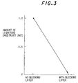
- FIG.3 shows an amount of lithium mixture into the SiO2 buffer layer 3 depending on the existence of the lithium blocking layer 6, i.e., on the right end point of the horizontal axis, the lithium blocking layer is formed on the surface of the LiNbO3 crystalline substrate 1; on the left end point of the horizontal axis, the lithium blocking layer is not formed on the surface of the LiNbO3 crystalline substrate 1.
- the SiO2 buffer layer 3 is formed by the sputtering method. Due to the lithium blocking layer 6, the amount of lithium mixture into the SiO2 buffer layer is reduced to about 1/50.
- the lithium mixture from the LiNbO3 crystalline substrate 1 into the SiO2 buffer layer 3 due to plasma or heat when the SiO2 buffer layer 3 is deposited by CVD method, sputtering method, vapor deposition method or the like can be effectively reduced.
- the DC drift of the device can be suppressed to provide an optical control device with high reliability.
- the above optical control device can be obtained if only the amount and depth of metal doped is set such that the channel-type optical waveguides 2a and 2b serve as a waveguide, i.e., the amount, depth and type of metal doped are not limited by the other condition.
- an optical control device in the second preferred embodiment will be explained.
- an optical circuit 5 is a directional coupler, and a lithium blocking layer 6 is formed on the surface a crystalline substrate 1 except the region where the waveguided-light through channel-type optical waveguides 2a and 2b propagates.
- the lithium blocking layer 6 is not formed at the region between the channel-type optical waveguides 2a and 2b of the directional coupler, since the waveguided-light propagates therebetween.
- the second embodiment can provide a similar advantage to that of the first embodiment.
- the optical control device in the second embodiment does not affect the propagation characteristic of the waveguided-light through the channel-type optical waveguides 2a and 2b. Therefore, reduction of the steps in processing and designing of the device, and a higher yield can be realized.
- channel-type optical waveguides 2a and 2b are formed on the surface of a LiTaO3 crystalline substrate 1 by the proton exchanging, and a lithium blocking layer 6 is formed by doping metal on the entire surface of the LiTaO3 crystalline substrate 1.
- the proton exchanging for forming the channel-type optical waveguides 2a and 2b may employ benzoic acid, pyrophosphoric acid or the like.
- the crystalline substrate 1 is made of LiTaO3
- the lithium blocking layer 6 is doped by the ion implantation.
- the crystalline substrate 1 is made of LiNbO3
- the lithium blocking layer 6 is doped by the thermal diffusion or ion implantation.
- the doping metal for forming the lithium blocking layer 6 may include Ti, Cu, V, Fe, Mo, Cr or the like.
- the third embodiment can also provide a similar advantage to that of the first embodiment.
- the above optical control device can be obtained if only the proton exchanging and the metal doping into the lithium blocking layer 6 are performed such that the channel-type optical waveguides 2a and 2b serve as a waveguide, i.e., the amount and depth of the proton exchanging, and the amount, depth and type of metal doped are not limited by the other condition.
- FIGS. 6A and 6B show the process for making an optical control device in the first preferred embodiment according to the invention.
- a patterned metal layer 7a for forming channel-type optical waveguides 2a and 2b and a metal layer 7b for forming a lithium blocking layer 6 are formed (FIG.6A).
- the depositing of the metal layers 7a and 7b may be performed by CVD, sputtering, vapor deposition method or the like.
- the patterning of the metal layer 7a is by the standard lithography technique.
- the metal layer 7b for the lithium blocking layer 6 may be patterned such that the region for propagating waveguided-light without the lithium blocking layer is left.
- the patterned metal layer 7a for forming the channel-type optical waveguides 2a and 2b is mounted on the metal layer 7b for forming the lithium blocking layer 6 in FIG.6A, it will be easily appreciated that the relationship in the mounting can be changed upside down, i.e., the metal layer 7b may be mounted on the metal layer 7a.
- the doping metal may include Ti, Cu, V, Fe, Mo, Cr or the like.
- both the channel-type optical waveguides 2a and 2b and lithium blocking layer 6 are formed by using titanium as the doping metal.
- FIGS. 7A and 7B show the process for making an optical control device in the second preferred embodiment according to the invention.
- a metal layer 7a for forming channel-type optical waveguides 2a and 2b as shown in FIG.6A on a LiNbO3 crystalline substrate 1 the metal layer 7a is processed by the thermal diffusion to form the channel-type optical waveguides 2a and 2b (FIG.7A).
- a metal layer 7b for forming a lithium blocking layer 6 as shown in FIG.6A on the LiNbO3 crystalline substrate 1 the metal layer 7b is processed by the thermal diffusion to form the lithium blocking layer 6 (FIG.7B).
- the metal layer 7b for the lithium blocking layer 6 may be patterned such that the region for propagating waveguided-light without the lithium blocking layer is left.
- the depositing of the metal layers 7a and 7b may be performed by CVD, sputtering, vapor deposition method or the like.
- the patterning of the metal layer 7a is by the standard lithography technique.
- the lithium blocking layer 6 is formed after the formation of the channel-type optical waveguides 2a and 2b, the lithium blocking layer 6 can be formed before the formation of the channel-type optical waveguides 2a and 2b.
- the above optical control device can be obtained if only the channel-type optical waveguides 2a and 2b serve as a waveguide, i.e., the relationship in depth between the channel-type optical waveguides 2a and 2b and the lithium blocking layer 6 is not limited by the other condition.
- the doping metal may include Ti, Cu, V, Fe, Mo, Cr or the like.
- both the channel-type optical waveguides 2a and 2b and lithium blocking layer 6 are formed by using titanium as the doping metal.
- the optical control device in the fourth embodiment is provided with an optical circuit 5 which has two channel-type optical waveguides 2a and 2b which are formed on a LiNbO3 crystalline substrate 1 by the thermal diffusion method, and electrodes 4a and 4b which are formed on a buffer layer 3 of optically transparent film and are disposed over the channel-type optical waveguides 2a and 2b.
- the optical circuit 5 may employ a directional-coupler type, mach-zender type, balance-bridge type or the like.
- the buffer layer 3 is preferably made of SiO2, and it also may be made of Al2O3, MgF2, SiON, Si3N4 or the like.
- the depositing of the buffer layer 3 may be performed by the CVD method, sputtering method, vapor deposition method or the like.
- the electrodes 4a and 4b may be made of various conductive materials such as Au, Al, Mo, Cu, WSi, ITO, ZnO or conductive polymer.
- a film layer 6 (hereinafter referred to as "lithium blocking layer") which is separated from the buffer layer 3 is provided.
- the lithium blocking layer 6 is not formed in the region for propagating waveguided-light.
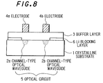
- the lithium blocking layer 6, as shown in FIG.8 is not formed on the channel-type optical waveguides 2a and 2b nor between the channel-type optical waveguides 2a and 2b.
- the lithium blocking layer 6 may be made of a metal or semiconductor material of a single element including Si, Ti, Cu, V, Fe, Mo, Cr or the like, or a dielectric, metal, semiconductor, organic material or the like which is difficult to generate the ionic polarization in applying an electric field, such as crystal doped by phosphorus, MgF2, Si3N4, WSi, GaAs, InP, polyimide.
- the substrate 1 is limited to the LiNbO3 crystalline substrate, and any lithium-containing crystalline substrate such as a LiTaO3 crystalline substrate may be used.
- the depositing of the lithium blocking layer 6 may be performed by CVD, sputtering, vapor deposition method or the like.
- the standard lithography technique is employed to preclude the formation of the lithium blocking layer at the region for propagating waveguided-light.
- a titanium-deposited layer with a thickness of 0.02 to 0.15 nm is processed by the thermal diffusion at 850 to 1100 °C for 0.5 to 20 hours to form the channel-type optical waveguides 2a and 2b.
- a lithium blocking layer 6 and buffer layer 3 between two channel-type optical waveguides 2a and 2b is partially removed.
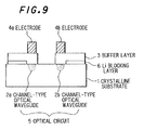
- This structure is suitable for the case that the lithium blocking layer 6 between the channel-type optical waveguides 2a and 2b is not proper, i.e., when the optical circuit 5 is a directional coupler, X-type or the like. Because the covering area of the lithium blocking layer 6 is greater than that of the lithium blocking layer 6 in the fourth embodiment, the lithium mixture into the buffer layer 3 when the buffer layer 3 is deposited can be more reduced to further suppress the DC drift and provide an optical control device with higher reliability.
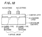
- This embodiment is suitable for the case that the optical circuit 5 in which waveguided-light does not propagate between two channel-type optical waveguides 2a and 2b, such as a mach-zender type, balance-bridge type is employed. Namely, a lithium blocking layer 6 is also formed between the channel-type optical waveguides 2a and 2b. Because the covering area of the lithium blocking layer 6 is greater than that of the lithium blocking layer 6 in the fourth embodiment, the lithium mixture into the buffer layer 3 when the buffer layer 3 is deposited can be more reduced to further suppress the DC drift and provide an optical control device with higher reliability.
- FIGS.11A to 11C show the process for making the optical device in the fifth embodiment.
- the lithium blocking layer 6 is deposited on the LiNbO3 crystalline substrate 1 except on the channel-type optical waveguides 2a and 2b.
- the lithium blocking layer 6 is deposited with chromium by the electron-beam vapor deposition, thermal deposition, sputtering method or the like. Thereafter, the lithium blocking layer 6 corresponding to the region where the electrodes 4a and 4b will be provided is removed by using the standard photolithography technique and etching.
- SiO2 is deposited thereon to form a buffer layer 3, by CVD, sputtering method or the like.
- the buffer layer 3 may be annealed.
- the lithium blocking layer 6 and buffer layer 3 between the channel-type optical waveguides 2a and 2b are removed by using the standard photolithography technique and etching.
- the layer for forming the electrodes 4a and 4b is deposited by the electron-beam vapor deposition, thermal vapor deposition, sputtering method or the like, thereafter forming the electrodes 4a and 4b by using the standard photolithography technique and etching.
- the electrodes are mainly made of gold.
- the removing of the lithium blocking layer 6 and buffer layer 3 between the channel-type optical waveguides 2a and 2b as in FIG.11B may be simultaneously carried out after the forming of the electrodes 4a and 4b.
- the process for making the optical control devices in the fourth and sixth embodiments will be easily understood. Namely, after forming the directional coupler 5 of two waveguides 2a and 2b on the LiNbO3 crystalline substrate 1 by the thermal diffusion, the layer for forming the lithium blocking layer 6 is deposited. Thereafter, the lithium blocking layer 6 corresponding to the region where the electrodes 4a and 4b will be formed or the lithium blocking layer 6 corresponding to the above-mentioned region and the region between the electrodes 4a and 4b is removed. Thereafter, the buffer layer 3 is deposited thereon. Finally, similarly to the fifth embodiment, the electrodes 4a and 4b are formed on the buffer layer 3.
- FIG.12 shows an amount of lithium mixture into the SiO2 buffer layer 3 depending on the existence of the lithium blocking layer 6, i.e., on the right end point of the horizontal axis, the lithium blocking layer is formed on the surface of the LiNbO3 crystalline substrate 1 (in the fourth to sixth embodiments); on the left end point of the horizontal axis, the lithium blocking layer is not formed on the surface of the LiNbO3 crystalline substrate 1.
- the SiO2 buffer layer 3 is formed by the sputtering method. Due to the lithium blocking layer 6, the amount of lithium mixture into the SiO2 buffer layer 3 is reduced to about 1/50.
- the lithium mixture from the LiNbO3 crystalline substrate 1 into the SiO2 buffer layer 3 due to plasma or heat when the SiO2 buffer layer 3 is deposited by CVD method, sputtering method, vapor deposition method or the like can be effectively reduced.
Landscapes
- Physics & Mathematics (AREA)
- Nonlinear Science (AREA)
- Chemical & Material Sciences (AREA)
- Engineering & Computer Science (AREA)
- Ceramic Engineering (AREA)
- Crystallography & Structural Chemistry (AREA)
- General Physics & Mathematics (AREA)
- Optics & Photonics (AREA)
- Optical Integrated Circuits (AREA)
Applications Claiming Priority (4)
| Application Number | Priority Date | Filing Date | Title |
|---|---|---|---|
| JP6231754A JP2809112B2 (ja) | 1994-09-27 | 1994-09-27 | 光制御デバイスとその製造方法 |
| JP231754/94 | 1994-09-27 | ||
| JP292625/94 | 1994-11-28 | ||
| JP6292625A JP2624199B2 (ja) | 1994-11-28 | 1994-11-28 | 光制御デバイスとその製造方法 |
Publications (2)
| Publication Number | Publication Date |
|---|---|
| EP0704742A2 true EP0704742A2 (de) | 1996-04-03 |
| EP0704742A3 EP0704742A3 (de) | 1997-07-23 |
Family
ID=26530069
Family Applications (1)
| Application Number | Title | Priority Date | Filing Date |
|---|---|---|---|
| EP95306831A Withdrawn EP0704742A3 (de) | 1994-09-27 | 1995-09-27 | Optische Steuervorrichtung und Verfahren zu ihrer Herstellung |
Country Status (3)
| Country | Link |
|---|---|
| US (1) | US5687265A (de) |
| EP (1) | EP0704742A3 (de) |
| CA (1) | CA2159129C (de) |
Cited By (1)
| Publication number | Priority date | Publication date | Assignee | Title |
|---|---|---|---|---|
| GB2330664A (en) * | 1997-10-21 | 1999-04-28 | Integrated Optical Components | Integrated optical devices |
Families Citing this family (6)
| Publication number | Priority date | Publication date | Assignee | Title |
|---|---|---|---|---|
| US6404944B1 (en) * | 2000-03-17 | 2002-06-11 | Unveristy Of Central Florida | Monolithic integrated active semiconductor optical switch for a 1×N interconnect switch |
| GB0101343D0 (en) * | 2001-01-19 | 2001-03-07 | Secr Defence | Electro-optic waveguide device |
| WO2004107466A1 (ja) * | 2003-05-08 | 2004-12-09 | Matsushita Electric Industrial Co. Ltd. | 電気スイッチおよびそれを用いた記憶素子 |
| CN100428520C (zh) * | 2003-05-08 | 2008-10-22 | 松下电器产业株式会社 | 电气开关及使用该电气开关的存储元件 |
| TWI424200B (zh) * | 2008-12-31 | 2014-01-21 | Ind Tech Res Inst | 色彩分離光學元件以及所應用的影像裝置 |
| US9223158B2 (en) * | 2011-07-19 | 2015-12-29 | Sumitomo Osaka Cement Co., Ltd. | Optical waveguide element and method of manufacturing the same |
Family Cites Families (10)
| Publication number | Priority date | Publication date | Assignee | Title |
|---|---|---|---|---|
| US4561718A (en) * | 1983-08-22 | 1985-12-31 | Sperry Corporation | Photoelastic effect optical waveguides |
| JPS6396626A (ja) * | 1986-10-14 | 1988-04-27 | Nec Corp | 導波型光制御素子 |
| EP0315350A1 (de) * | 1987-11-02 | 1989-05-10 | AT&T Corp. | Technik zum intrinsischen Gettern bei niedriger Temperatur |
| US5042895A (en) * | 1988-01-19 | 1991-08-27 | E. I. Du Pont De Nemours And Company | Waveguide structure using potassium titanyl phosphate |
| JP3139712B2 (ja) * | 1990-11-28 | 2001-03-05 | 日本電気株式会社 | 光制御デバイス |
| JPH0566428A (ja) * | 1991-09-05 | 1993-03-19 | Nec Corp | 光制御デバイス |
| JPH05113513A (ja) * | 1991-10-23 | 1993-05-07 | Fujitsu Ltd | 導波路型光デバイスおよびその製造方法 |
| EP0553568B1 (de) * | 1991-12-27 | 1998-08-26 | Fujitsu Limited | Optische Wellenleiteranordnung mit reduzierter DC-Drift |
| US5390157A (en) * | 1992-07-15 | 1995-02-14 | Eastman Kodak Company | Waveguide optical pick-up head using mach-zehnder interferometer wavefront sensor apparatus and method |
| JPH0675195A (ja) * | 1992-08-17 | 1994-03-18 | Nec Corp | 光制御デバイス |
-
1995
- 1995-09-26 CA CA002159129A patent/CA2159129C/en not_active Expired - Fee Related
- 1995-09-27 US US08/535,477 patent/US5687265A/en not_active Expired - Lifetime
- 1995-09-27 EP EP95306831A patent/EP0704742A3/de not_active Withdrawn
Non-Patent Citations (1)
| Title |
|---|
| H. NISHIMOTO ET AL.: "Polarization Independent 8x8 LiNb03 Optical Matrix Switch", ELECTRONIC INFORMATION COMMUNICATION SOCIETY, vol. OQE88, no. 147, pages 67 - 74 |
Cited By (2)
| Publication number | Priority date | Publication date | Assignee | Title |
|---|---|---|---|---|
| GB2330664A (en) * | 1997-10-21 | 1999-04-28 | Integrated Optical Components | Integrated optical devices |
| GB2330664B (en) * | 1997-10-21 | 2002-01-23 | Integrated Optical Components | The manufacture of integrated optical devices |
Also Published As
| Publication number | Publication date |
|---|---|
| EP0704742A3 (de) | 1997-07-23 |
| CA2159129A1 (en) | 1996-03-28 |
| US5687265A (en) | 1997-11-11 |
| CA2159129C (en) | 1999-11-30 |
Similar Documents
| Publication | Publication Date | Title |
|---|---|---|
| JP4703627B2 (ja) | 1×2偏波スプリッタおよび1×2偏波無依存型光スイッチ | |
| US7529433B2 (en) | Humidity tolerant electro-optic device | |
| US6055342A (en) | Integrated optical intensity modulator and method for fabricating the same | |
| JP2674535B2 (ja) | 光制御デバイス | |
| JP2713087B2 (ja) | 導波形光デバイス | |
| US4983006A (en) | Polarization-independent optical waveguide switch | |
| EP0713123B1 (de) | Optische Steuervorrichtung | |
| US5687265A (en) | Optical control device and method for making the same | |
| JP2002122834A (ja) | 光導波路素子 | |
| CA2256216C (en) | Optical control device and method for making the same | |
| JP2717980B2 (ja) | 集積化光導波路デバイス | |
| JPH0675195A (ja) | 光制御デバイス | |
| JP2624199B2 (ja) | 光制御デバイスとその製造方法 | |
| JP2809112B2 (ja) | 光制御デバイスとその製造方法 | |
| JP2850899B2 (ja) | 光制御デバイス | |
| JPS6396626A (ja) | 導波型光制御素子 | |
| JPH0721597B2 (ja) | 光スイッチ | |
| JPH01201628A (ja) | 光スイッチ | |
| JP3050202B2 (ja) | 光導波路デバイスおよびその製造方法 | |
| JP2812320B2 (ja) | 集積化光回路とその製造方法 | |
| JPS63250611A (ja) | 光導波路の製造方法 | |
| KAWANO | Improvement of the Performance of a Shielded Velocity-Matched Ti: LiNbO 3 Optical Modulator by Using a Ridge Structure | |
| JPH0293423A (ja) | 光導波路デバイス | |
| JPS6060622A (ja) | 光導波路 | |
| JPS6370827A (ja) | 光制御デバイスの製造方法 |
Legal Events
| Date | Code | Title | Description |
|---|---|---|---|
| PUAI | Public reference made under article 153(3) epc to a published international application that has entered the european phase |
Free format text: ORIGINAL CODE: 0009012 |
|
| AK | Designated contracting states |
Kind code of ref document: A2 Designated state(s): DE FR GB SE |
|
| 17P | Request for examination filed |
Effective date: 19960307 |
|
| PUAL | Search report despatched |
Free format text: ORIGINAL CODE: 0009013 |
|
| AK | Designated contracting states |
Kind code of ref document: A3 Designated state(s): DE FR GB SE |
|
| STAA | Information on the status of an ep patent application or granted ep patent |
Free format text: STATUS: THE APPLICATION HAS BEEN WITHDRAWN |
|
| 18W | Application withdrawn |
Effective date: 20030611 |