EP0704770A2 - Procédé de support de fabrication d'images sur une plaque d'impression et plaque d'impression utilisée dans tel procédé - Google Patents
Procédé de support de fabrication d'images sur une plaque d'impression et plaque d'impression utilisée dans tel procédé Download PDFInfo
- Publication number
- EP0704770A2 EP0704770A2 EP95114848A EP95114848A EP0704770A2 EP 0704770 A2 EP0704770 A2 EP 0704770A2 EP 95114848 A EP95114848 A EP 95114848A EP 95114848 A EP95114848 A EP 95114848A EP 0704770 A2 EP0704770 A2 EP 0704770A2
- Authority
- EP
- European Patent Office
- Prior art keywords
- layer
- electrode
- ferroelectric
- field strength
- frequency
- Prior art date
- Legal status (The legal status is an assumption and is not a legal conclusion. Google has not performed a legal analysis and makes no representation as to the accuracy of the status listed.)
- Granted
Links
Images
Classifications
-
- B—PERFORMING OPERATIONS; TRANSPORTING
- B41—PRINTING; LINING MACHINES; TYPEWRITERS; STAMPS
- B41C—PROCESSES FOR THE MANUFACTURE OR REPRODUCTION OF PRINTING SURFACES
- B41C1/00—Forme preparation
- B41C1/10—Forme preparation for lithographic printing; Master sheets for transferring a lithographic image to the forme
- B41C1/1058—Forme preparation for lithographic printing; Master sheets for transferring a lithographic image to the forme by providing a magnetic pattern, a ferroelectric pattern or a semiconductive pattern, e.g. by electrophotography
-
- G—PHYSICS
- G03—PHOTOGRAPHY; CINEMATOGRAPHY; ANALOGOUS TECHNIQUES USING WAVES OTHER THAN OPTICAL WAVES; ELECTROGRAPHY; HOLOGRAPHY
- G03G—ELECTROGRAPHY; ELECTROPHOTOGRAPHY; MAGNETOGRAPHY
- G03G13/00—Electrographic processes using a charge pattern
- G03G13/056—Electrographic processes using a charge pattern using internal polarisation
-
- G—PHYSICS
- G03—PHOTOGRAPHY; CINEMATOGRAPHY; ANALOGOUS TECHNIQUES USING WAVES OTHER THAN OPTICAL WAVES; ELECTROGRAPHY; HOLOGRAPHY
- G03G—ELECTROGRAPHY; ELECTROPHOTOGRAPHY; MAGNETOGRAPHY
- G03G13/00—Electrographic processes using a charge pattern
- G03G13/26—Electrographic processes using a charge pattern for the production of printing plates for non-xerographic printing processes
-
- G—PHYSICS
- G03—PHOTOGRAPHY; CINEMATOGRAPHY; ANALOGOUS TECHNIQUES USING WAVES OTHER THAN OPTICAL WAVES; ELECTROGRAPHY; HOLOGRAPHY
- G03G—ELECTROGRAPHY; ELECTROPHOTOGRAPHY; MAGNETOGRAPHY
- G03G5/00—Recording-members for original recording by exposure, e.g. to light, to heat or to electrons; Manufacture thereof; Selection of materials therefor
- G03G5/02—Charge-receiving layers
-
- G—PHYSICS
- G03—PHOTOGRAPHY; CINEMATOGRAPHY; ANALOGOUS TECHNIQUES USING WAVES OTHER THAN OPTICAL WAVES; ELECTROGRAPHY; HOLOGRAPHY
- G03G—ELECTROGRAPHY; ELECTROPHOTOGRAPHY; MAGNETOGRAPHY
- G03G5/00—Recording-members for original recording by exposure, e.g. to light, to heat or to electrons; Manufacture thereof; Selection of materials therefor
- G03G5/02—Charge-receiving layers
- G03G5/022—Layers for surface-deformation imaging, e.g. frost imaging
Definitions
- the invention relates to methods for supporting the imaging of a printing form with at least a first layer that a photo effect, d. H. contains the photoferroelectric effect, showing the ferroelectric, wherein free charge carriers are generated in the ferroelectric by irradiation with light above the photo-effect cutoff frequency of the ferroelectric.
- the invention also relates to a method in which the free charge carriers are generated by the photo effect in a non-ferroelectric layer which is adjacent to a ferroelectric layer to be imaged, this layer being only the charge-generating layer of a photoconductor composed of several layers and therefore does not represent a photoconductor according to the usual definition.
- the invention also relates to a printing form, the ferroelectric layer of which is specially designed to enhance the photoferroelectric effect.
- a printing form which is designed as a thin disk or plate with a ferroelectric material and a photoconductive coating on one of its surfaces.
- a first electrode is arranged in terms of area, and a second electrode is applied to the photoconductive coating.
- the photoelectric layer acts as a switch. At least one of the two electrodes is removable. At least the electrode on the photoconductive coating is translucent. If an optical image is focused on the photoconductive surface of the printing form and at the same time an electrical voltage is applied to the two electrodes, the ferroelectric can be polarized imagewise.
- the surface thereof can also be scanned by a bundled light beam, for example a laser beam.
- a direct voltage is applied to the two electrodes at the same time, the specific electrical resistance of the photoconductive coating is low. Therefore, the DC voltage mainly affects those areas of the ferroelectric which are below the bright image areas of the photoconductive coating.
- the specific electrical resistance of the photoconductive coating remains high in the dark areas of the image. As a result, ferroelectric polarization is induced in the ferroelectric only in those areas which correspond to the bright image areas.
- a printing method using a pyroelectric film is known from US Pat. No. 3,899,969.
- ferroelectric materials e.g. B. lead zirconate titanate or polyvinylidene fluoride used.
- Such a ferroelectric is placed, for example, between two planar electrodes, one of which is translucent.
- a voltage is applied between the two electrodes, and the ferroelectric film is selectively heated by electromagnetic radiation in accordance with an image pattern to be generated in it.
- the ferroelectric is permanently polarized in terms of image by the areal application of the electric field and the selective heating.
- the complex, not always easily controllable photothermal effect is used.
- the photo effect in a ferroelectric layer ie the photoferroelectric effect
- the photo effect can also be used in a layer adjacent to a ferroelectric, which, in contrast to the photoconductive layers known from DT 25 30 290 Al, only consists of a functional component of such a photoconductive layer, which alone does not have a functional photoconductor represents.
- a ferroelectric for imaging can also be irradiated with light of other, even lower frequencies, in addition to light that exceeds the cutoff frequency, in order to increase the temperature of the ferroelectric material, i. H. through the photothermal effect to support the polarization of the ferroelectric.
- the invention creates printing forms which are particularly suitable for using the photoferroelectric effect.
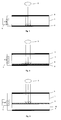
- a printing form (FIG. 1) has a ferroelectric layer 1.
- Layer 1 consists for example of lead zirconate titanate (PZT) or of lead lanthanum zirconate titanate (PLZT) or of a ceramic containing a ferroelectric.
- the underside of layer 1 is covered over its entire area by an electrode 2.
- layer 1 is also covered by an all-over electrode 3.
- the electrode 3 is translucent and removable, it consists for example of a transparent film coated with indium oxide (In2O3) or tin oxide (SnO2).
- An external voltage U ext generated by a voltage source 4 is present between the electrodes 2 and 3. After the irradiation, the electrode 3 is removed again.
- the layer 1 through the translucent electrode 3 with light, for. B. near UV light, irradiated.
- This light has sufficient energy, ie its frequency lies above a material-specific cutoff frequency in order to produce the photo effect (photoferroelectric effect) in the ferroelectric layer 1.
- the photoferroelectric effect is based on the same physical principle as, for example, the photo effect in pn junctions of semiconductors. In the case of these semiconductors, an electrical field is created in the pn junction by diffusion of the excess charge carriers, which produces a zone free of charge carriers, the so-called barrier layer. If new charge carriers are generated in this zone by means of the photo effect, photoconductivity arises.
- a polarized ferroelectric With a polarized ferroelectric, a comparable barrier layer is created on both surfaces by an electric field between the oriented domains and the polarization charge necessary to shield this field. If light is absorbed in this surface layer, free charge carriers are generated.
- the charge carriers migrate in accordance with the effect of the field and produce one stable, permanent space charge field. Its strength depends on the number of charge carriers generated by the photo effect and therefore on the duration and intensity of the irradiation, provided that the cutoff frequency for the photo effect is exceeded.
- the space charge field is superimposed on the applied field and supports the polarization of the ferroelectric, ie the coercive field strength required for reorienting the ferroelectric domains is reduced by the space charge field.
- FIG. 2 there is a further layer 6 containing a ferroelectric.
- the ferroelectric for layer 6 is chosen so that its coercive field strength lies above the coercive field strength of layer 1. Therefore, if an electrical field is applied between the electrodes 2 and 3 by the voltage source 4, the strength of which is above the coercive field strength of layer 1 but below the coercive field strength of layer 6, this acts as long as the printing form is not irradiated with light Isolator and prevents polarization. Only when the layer 6 is irradiated with light whose frequency is above the photo-effect cutoff frequency of the ferroelectric of the layer 6 does it become electrically conductive or polarizable according to the process shown in FIG. 1 and also allows the polarization of the layer 1. The printing form can then be exposed imagewise with the light source 5. The prerequisite for this is that layer 1 is transparent to light of this frequency.
- the underside of the ferroelectric layer 1 is covered by a layer 7 instead of the electrode 2, which layer serves as a charge generator generation layer (charge generator layer).
- charge generator layer Such layers are known from organic multilayer photoconductors (multilayer OPC), which are generally made up of a very thin charge generator layer and a relatively thick charge transport layer. It is thereby achieved that as many charge carriers as possible generated by the photo effect are drawn into the transport layer which is insensitive to recombination before recombination. In the ferroelectric, this "charge transport layer" is the charge carrier-free zone immediately adjacent to the surface.
- the layer 7 is imagewise irradiated by the light source 5 with light of a frequency sufficient to produce the photo effect in the layer 7, charge carriers are generated there, provided the layer 1 is transparent to this light.
- the electrode 3 is at a certain potential in relation to the electrode 2, the free charge carriers that arise in the layer 7 migrate into the layer 1 due to the electric field in the direction of the electrode 3.
- a carrier layer 10 lies between the electrode 2 and the layer 7. The field strength is dependent on the number of charge carriers generated and the potential between the electrode 3 and the electrode 2. If the field strength that arises thereby exceeds the coercive field strength of the layer 1, this becomes polarized imagewise.
- the frequency required for the photo effect in layer 7 is still above the cut-off frequency required for the photoferroelectric effect in layer 1, because in this way the photo effect in layer 7 is still supported by the photoferroelectric effect in layer 1. If the printing form is irradiated directly from below onto the layer 7 instead of from above through the electrode 3 and the layer 1, the ferroelectric layer 1 can also be polarized, in which case the layer 1 and the electrode 3 need not be translucent.
- ferroelectric layers instead of a single layer 1, a plurality of ferroelectric layers which show the photoferroelectric effect can be provided. In addition to these, there may be further ferroelectric layers which, at least at the frequency of the incident light, do not show the photoferroelectric effect.
- the ferroelectric layers have, for example, a multi-layer structure, as is known per se with photo elements. The layers can be selected so that a first one of them has a strong photoferroelectric effect for the incident light and another shows a high conductivity for the electrons generated from the first layer or a good polarizability.
- Layer 1 is not necessarily translucent. It is also sufficient if the photons are already absorbed in the area immediately below the electrode 3 or above the electrode 2, if the layer is irradiated from below and the electrode 2 is translucent, in order to generate free electrons.
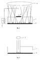
- a printing form is irradiated with the ferroelectric layer 1 and the electrode 2 covering the entire surface thereof by a light source 8.
- a light source 8 lies on the top of the layer 1 a transparent imaging electrode 9.
- a voltage U ext is present between the electrode 2 and the imaging electrode 9 through the voltage source 4. Due to the whole-area irradiation of the layer 1, the coercive field strength in the layer 1 is reduced due to the photoferroelectric effect, as a result of which the field strength required for polarization and thus the voltage U ext to be generated by the voltage source 4 is also reduced.
- the risk of electrical arcing between the individual imaging electrodes 9 is reduced because of the lower voltage.
- a higher image resolution can be achieved in which the imaging electrodes 9 can be combined on a smaller area at a lower voltage.
- FIG. 5 Another printing form (FIG. 5) is first polarized over the entire surface by applying a voltage U ext between the electrode 2 and the removable electrode 3 (not shown here). After removal of the electrode 3, the printing form is irradiated imagewise so that a sufficiently high conductivity arises over the entire thickness of the polarized layer 1, ie the photoferroelectric effect is exploited by irradiating the layer 1 with light above the limit frequency required for this effect .
- the prerequisite for this is that layer 1 is so thin that the charge carriers generated inside can migrate from the upper boundary layer to the lower one before recombination takes place. As a result, the layer 1 becomes sufficiently conductive so that the free charges present on its surface 10, which had been generated during polarization, flow out through the layer 1 onto the electrode 2. Accordingly, the printing form is depolarized at the locations irradiated by the radiation source 5. In contrast to the exemplary embodiments shown in FIGS. 1-4, a negative image is produced.
- the generation of the image can be supported by the photothermal effect known per se, in that the radiation source 5, 9 also emits low-energy light in addition to the light of sufficient energy required for the photoferroelectric effect that layer 1 is heated.
- the marginal energy of the radiation required for the photoferroelectric effect can be reduced by implanting foreign atoms in the boundary layer.
- the photosensitivity can be shifted far into the visible space if the layer 1 is previously with noble gas ions (Ne, He or Ar ions) in conjunction with Al- at least on the side from which the light penetrates into it. or has been implanted with Cr ions.
- the invention provides a printing form with a ferroelectric layer 1 in which, using the photoferroelectric effect in layer 1 or the photo effect in a layer 7 adjacent to layer 1, which is neither ferroelectric, nor has the function of a photoconductor , layer 1 imaging is supported by polarization or depolarization.
Landscapes
- Physics & Mathematics (AREA)
- General Physics & Mathematics (AREA)
- Engineering & Computer Science (AREA)
- Manufacturing & Machinery (AREA)
- Electrophotography Using Other Than Carlson'S Method (AREA)
- Manufacture Or Reproduction Of Printing Formes (AREA)
- Photoreceptors In Electrophotography (AREA)
- Thermal Transfer Or Thermal Recording In General (AREA)
Applications Claiming Priority (2)
| Application Number | Priority Date | Filing Date | Title |
|---|---|---|---|
| DE4434766 | 1994-09-29 | ||
| DE4434766A DE4434766A1 (de) | 1994-09-29 | 1994-09-29 | Verfahren zum Unterstützen der Bebilderung einer Druckform und Druckform zur Verwendung in einem der Verfahren |
Publications (3)
| Publication Number | Publication Date |
|---|---|
| EP0704770A2 true EP0704770A2 (fr) | 1996-04-03 |
| EP0704770A3 EP0704770A3 (fr) | 1997-05-07 |
| EP0704770B1 EP0704770B1 (fr) | 2000-02-09 |
Family
ID=6529479
Family Applications (1)
| Application Number | Title | Priority Date | Filing Date |
|---|---|---|---|
| EP95114848A Expired - Lifetime EP0704770B1 (fr) | 1994-09-29 | 1995-09-21 | Procédé de support de fabrication d'images sur une plaque d'impression et plaque d'impression utilisée dans tel procédé |
Country Status (5)
| Country | Link |
|---|---|
| US (1) | US5900341A (fr) |
| EP (1) | EP0704770B1 (fr) |
| JP (1) | JP2914899B2 (fr) |
| CA (1) | CA2157810C (fr) |
| DE (2) | DE4434766A1 (fr) |
Cited By (1)
| Publication number | Priority date | Publication date | Assignee | Title |
|---|---|---|---|---|
| US5927206A (en) * | 1997-12-22 | 1999-07-27 | Eastman Kodak Company | Ferroelectric imaging member and methods of use |
Families Citing this family (1)
| Publication number | Priority date | Publication date | Assignee | Title |
|---|---|---|---|---|
| TWI580956B (zh) * | 2015-12-17 | 2017-05-01 | 長庚大學 | 即時二維電位顯像方法 |
Citations (2)
| Publication number | Priority date | Publication date | Assignee | Title |
|---|---|---|---|---|
| US3899969A (en) | 1973-08-06 | 1975-08-19 | Minnesota Mining & Mfg | Printing using pyroelectric film |
| DE2530290A1 (de) | 1974-07-08 | 1976-01-22 | Hitachi Ltd | Verfahren und vorrichtung zum kopieren |
Family Cites Families (10)
| Publication number | Priority date | Publication date | Assignee | Title |
|---|---|---|---|---|
| CA944427A (en) * | 1968-11-21 | 1974-03-26 | Joseph Gaynor | Thermal electret copying process |
| US3700436A (en) * | 1969-02-28 | 1972-10-24 | Owens Illinois Inc | Electrode configuration for electrophotography |
| US3928031A (en) * | 1970-08-10 | 1975-12-23 | Katsuragawa Denki Kk | Method of electrophotography |
| JPS50115830A (fr) * | 1974-02-22 | 1975-09-10 | ||
| JPS57104948A (en) * | 1980-12-23 | 1982-06-30 | Olympus Optical Co Ltd | Multi-sheet copying electrophotographic method |
| JPH0629977B2 (ja) * | 1981-06-08 | 1994-04-20 | 株式会社半導体エネルギー研究所 | 電子写真用感光体 |
| JPS58139561A (ja) * | 1982-02-15 | 1983-08-18 | Canon Inc | 静電潜像読出し方法 |
| JP2581060B2 (ja) * | 1987-03-09 | 1997-02-12 | ミノルタ株式会社 | 潜像形成方法 |
| JP2965616B2 (ja) * | 1990-04-17 | 1999-10-18 | 株式会社リコー | 画像記録体及び画像記録方法 |
| JPH05224491A (ja) * | 1991-09-25 | 1993-09-03 | Ricoh Co Ltd | 画像記録方法 |
-
1994
- 1994-09-29 DE DE4434766A patent/DE4434766A1/de not_active Withdrawn
-
1995
- 1995-09-08 CA CA002157810A patent/CA2157810C/fr not_active Expired - Fee Related
- 1995-09-21 DE DE59507775T patent/DE59507775D1/de not_active Expired - Fee Related
- 1995-09-21 EP EP95114848A patent/EP0704770B1/fr not_active Expired - Lifetime
- 1995-09-28 JP JP7251585A patent/JP2914899B2/ja not_active Expired - Fee Related
-
1997
- 1997-09-03 US US08/922,742 patent/US5900341A/en not_active Expired - Fee Related
Patent Citations (2)
| Publication number | Priority date | Publication date | Assignee | Title |
|---|---|---|---|---|
| US3899969A (en) | 1973-08-06 | 1975-08-19 | Minnesota Mining & Mfg | Printing using pyroelectric film |
| DE2530290A1 (de) | 1974-07-08 | 1976-01-22 | Hitachi Ltd | Verfahren und vorrichtung zum kopieren |
Cited By (1)
| Publication number | Priority date | Publication date | Assignee | Title |
|---|---|---|---|---|
| US5927206A (en) * | 1997-12-22 | 1999-07-27 | Eastman Kodak Company | Ferroelectric imaging member and methods of use |
Also Published As
| Publication number | Publication date |
|---|---|
| JPH08123164A (ja) | 1996-05-17 |
| US5900341A (en) | 1999-05-04 |
| JP2914899B2 (ja) | 1999-07-05 |
| CA2157810A1 (fr) | 1996-03-30 |
| EP0704770B1 (fr) | 2000-02-09 |
| DE4434766A1 (de) | 1996-04-04 |
| DE59507775D1 (de) | 2000-03-16 |
| EP0704770A3 (fr) | 1997-05-07 |
| CA2157810C (fr) | 2000-09-05 |
Similar Documents
| Publication | Publication Date | Title |
|---|---|---|
| DE2836854C2 (fr) | ||
| DE1237902B (de) | Elektrophotographisches Aufzeichnungsmaterial und elektrophotographisches Verfahren unter Verwendung dieses Aufzeichnungsmaterials | |
| DE1804064A1 (de) | Elektrografisches Verfahren | |
| DE1932353B2 (de) | Verfahren und vorrichtung zur herstellung eines ladungsbildes auf einem elektrofotografischen aufzeichnungsmaterial | |
| EP0704770B1 (fr) | Procédé de support de fabrication d'images sur une plaque d'impression et plaque d'impression utilisée dans tel procédé | |
| DE2462398A1 (de) | Elektrophotographisches verfahren | |
| DE2737052A1 (de) | Fotogesteuerte ionenstrom-elektronenradiografie | |
| EP0340866A2 (fr) | Dispositif de production d'images radiologiques au moyen de photoconducteurs | |
| DE2752679C3 (de) | Verfahren und Vorrichtung zum Abtasten einer pyroelektrischen Speicherplatte | |
| DE2557685A1 (de) | Verfahren zur herstellung einer gerasterten photoleiterschicht | |
| DE2839994A1 (de) | Vorrichtung zur radiographischen analyse | |
| DE2809017C3 (de) | Verfahren zum Herstellen von mehreren Kopien einer Vorlage | |
| DE1950028A1 (de) | Elektrofotografische Druck- oder Kopiervorrichtung | |
| DE1549144B2 (de) | Informationsspeichereinrichtung und diese verwendendes Verfahren zur Speicherung von Informationen | |
| DE3139109A1 (de) | "elektrophotographisches kopierverfahren" | |
| DE1963615A1 (de) | Verfahren zur Erzeugung eines elektrostatischen Bildes in der elektronischen Photographie und Vorrichtung zur Durchfuehrung dieses Verfahrens | |
| DE2825399C2 (de) | Elektrophotographisches Kopierverfahren sowie fotoleitfähiges Steuergitter | |
| DE1906329C (de) | Verfahren zur röntgenelektrofotografischen Herstellung eines Ladungs bildes und eiektrofotografisches Aufzeichnungsmaterial zur Durchführung des Verfahrens | |
| DE1022091B (de) | Lichtempfindliches xerographisches Material | |
| DE1597880C3 (de) | Verfahren zum Verstärken der Ladungsunterschiede eines Ladungsbildes | |
| DE2929986A1 (de) | Verfahren und vorrichtung fuer die elektrostatische aufzeichnung | |
| DE2225767C3 (de) | Elektroradiografische Vorrichtung zum Herabsetzen der Verschmierung von durch Belichtung mittels durchdringender Strahlung geschaffenen latenten Abbildungen | |
| DE2126549C3 (de) | Elektrofotografisches Aufzeichnungsmaterial | |
| DE2947929A1 (de) | System und verfahren zur ausbildung eines elektrischen ladungsbildes auf der isolierschicht einer schichtanordnung aus einer isolierschicht, einer photoleitfaehigen und einer leitfaehigen schicht | |
| DE1537566C (de) | Anordnung zur Bildaufnahme , Bildspei cherung und Bildauswertung sowie Verfahren mit einer solchen Anordnung |
Legal Events
| Date | Code | Title | Description |
|---|---|---|---|
| PUAI | Public reference made under article 153(3) epc to a published international application that has entered the european phase |
Free format text: ORIGINAL CODE: 0009012 |
|
| AK | Designated contracting states |
Kind code of ref document: A2 Designated state(s): CH DE FR GB IT LI NL |
|
| PUAL | Search report despatched |
Free format text: ORIGINAL CODE: 0009013 |
|
| AK | Designated contracting states |
Kind code of ref document: A3 Designated state(s): CH DE FR GB IT LI NL |
|
| 17P | Request for examination filed |
Effective date: 19970910 |
|
| GRAG | Despatch of communication of intention to grant |
Free format text: ORIGINAL CODE: EPIDOS AGRA |
|
| 17Q | First examination report despatched |
Effective date: 19990419 |
|
| GRAG | Despatch of communication of intention to grant |
Free format text: ORIGINAL CODE: EPIDOS AGRA |
|
| GRAH | Despatch of communication of intention to grant a patent |
Free format text: ORIGINAL CODE: EPIDOS IGRA |
|
| GRAH | Despatch of communication of intention to grant a patent |
Free format text: ORIGINAL CODE: EPIDOS IGRA |
|
| ITF | It: translation for a ep patent filed | ||
| GRAA | (expected) grant |
Free format text: ORIGINAL CODE: 0009210 |
|
| AK | Designated contracting states |
Kind code of ref document: B1 Designated state(s): CH DE FR GB IT LI NL |
|
| REG | Reference to a national code |
Ref country code: CH Ref legal event code: NV Representative=s name: E. BLUM & CO. PATENTANWAELTE Ref country code: CH Ref legal event code: EP |
|
| REF | Corresponds to: |
Ref document number: 59507775 Country of ref document: DE Date of ref document: 20000316 |
|
| GBT | Gb: translation of ep patent filed (gb section 77(6)(a)/1977) |
Effective date: 20000511 |
|
| ET | Fr: translation filed | ||
| PLBE | No opposition filed within time limit |
Free format text: ORIGINAL CODE: 0009261 |
|
| STAA | Information on the status of an ep patent application or granted ep patent |
Free format text: STATUS: NO OPPOSITION FILED WITHIN TIME LIMIT |
|
| 26N | No opposition filed | ||
| REG | Reference to a national code |
Ref country code: GB Ref legal event code: IF02 |
|
| PGFP | Annual fee paid to national office [announced via postgrant information from national office to epo] |
Ref country code: NL Payment date: 20030828 Year of fee payment: 9 |
|
| PGFP | Annual fee paid to national office [announced via postgrant information from national office to epo] |
Ref country code: DE Payment date: 20040907 Year of fee payment: 10 |
|
| PGFP | Annual fee paid to national office [announced via postgrant information from national office to epo] |
Ref country code: CH Payment date: 20040909 Year of fee payment: 10 |
|
| PGFP | Annual fee paid to national office [announced via postgrant information from national office to epo] |
Ref country code: FR Payment date: 20040910 Year of fee payment: 10 |
|
| PGFP | Annual fee paid to national office [announced via postgrant information from national office to epo] |
Ref country code: GB Payment date: 20040913 Year of fee payment: 10 |
|
| PG25 | Lapsed in a contracting state [announced via postgrant information from national office to epo] |
Ref country code: NL Free format text: LAPSE BECAUSE OF NON-PAYMENT OF DUE FEES Effective date: 20050401 |
|
| NLV4 | Nl: lapsed or anulled due to non-payment of the annual fee |
Effective date: 20050401 |
|
| PG25 | Lapsed in a contracting state [announced via postgrant information from national office to epo] |
Ref country code: IT Free format text: LAPSE BECAUSE OF NON-PAYMENT OF DUE FEES;WARNING: LAPSES OF ITALIAN PATENTS WITH EFFECTIVE DATE BEFORE 2007 MAY HAVE OCCURRED AT ANY TIME BEFORE 2007. THE CORRECT EFFECTIVE DATE MAY BE DIFFERENT FROM THE ONE RECORDED. Effective date: 20050921 Ref country code: GB Free format text: LAPSE BECAUSE OF NON-PAYMENT OF DUE FEES Effective date: 20050921 |
|
| PG25 | Lapsed in a contracting state [announced via postgrant information from national office to epo] |
Ref country code: LI Free format text: LAPSE BECAUSE OF NON-PAYMENT OF DUE FEES Effective date: 20050930 Ref country code: CH Free format text: LAPSE BECAUSE OF NON-PAYMENT OF DUE FEES Effective date: 20050930 |
|
| PG25 | Lapsed in a contracting state [announced via postgrant information from national office to epo] |
Ref country code: DE Free format text: LAPSE BECAUSE OF NON-PAYMENT OF DUE FEES Effective date: 20060401 |
|
| REG | Reference to a national code |
Ref country code: CH Ref legal event code: PL |
|
| GBPC | Gb: european patent ceased through non-payment of renewal fee |
Effective date: 20050921 |
|
| PG25 | Lapsed in a contracting state [announced via postgrant information from national office to epo] |
Ref country code: FR Free format text: LAPSE BECAUSE OF NON-PAYMENT OF DUE FEES Effective date: 20060531 |
|
| REG | Reference to a national code |
Ref country code: FR Ref legal event code: ST Effective date: 20060531 |