EP0704835B1 - Fehlerdiffusionsfilter für eine DMD-Anzeige - Google Patents
Fehlerdiffusionsfilter für eine DMD-Anzeige Download PDFInfo
- Publication number
- EP0704835B1 EP0704835B1 EP95114890A EP95114890A EP0704835B1 EP 0704835 B1 EP0704835 B1 EP 0704835B1 EP 95114890 A EP95114890 A EP 95114890A EP 95114890 A EP95114890 A EP 95114890A EP 0704835 B1 EP0704835 B1 EP 0704835B1
- Authority
- EP
- European Patent Office
- Prior art keywords
- intensity
- micromirrors
- significant bits
- given
- pixel
- Prior art date
- Legal status (The legal status is an assumption and is not a legal conclusion. Google has not performed a legal analysis and makes no representation as to the accuracy of the status listed.)
- Expired - Lifetime
Links
- 238000009792 diffusion process Methods 0.000 title claims description 12
- 230000003111 delayed effect Effects 0.000 claims description 5
- 230000001934 delay Effects 0.000 claims description 4
- 239000004065 semiconductor Substances 0.000 claims description 2
- 230000008878 coupling Effects 0.000 claims 2
- 238000010168 coupling process Methods 0.000 claims 2
- 238000005859 coupling reaction Methods 0.000 claims 2
- 230000001902 propagating effect Effects 0.000 claims 2
- 230000001419 dependent effect Effects 0.000 claims 1
- 230000002708 enhancing effect Effects 0.000 claims 1
- 230000004044 response Effects 0.000 description 6
- 238000010586 diagram Methods 0.000 description 5
- 230000005540 biological transmission Effects 0.000 description 2
- 239000003086 colorant Substances 0.000 description 2
- 230000007547 defect Effects 0.000 description 2
- 230000006870 function Effects 0.000 description 2
- 238000000034 method Methods 0.000 description 2
- 230000015556 catabolic process Effects 0.000 description 1
- 230000002950 deficient Effects 0.000 description 1
- 238000006731 degradation reaction Methods 0.000 description 1
- 230000000694 effects Effects 0.000 description 1
- 238000003384 imaging method Methods 0.000 description 1
- 230000007935 neutral effect Effects 0.000 description 1
- 230000000644 propagated effect Effects 0.000 description 1
- 238000001228 spectrum Methods 0.000 description 1
- 230000003068 static effect Effects 0.000 description 1
Images



Classifications
-
- G—PHYSICS
- G09—EDUCATION; CRYPTOGRAPHY; DISPLAY; ADVERTISING; SEALS
- G09G—ARRANGEMENTS OR CIRCUITS FOR CONTROL OF INDICATING DEVICES USING STATIC MEANS TO PRESENT VARIABLE INFORMATION
- G09G3/00—Control arrangements or circuits, of interest only in connection with visual indicators other than cathode-ray tubes
- G09G3/20—Control arrangements or circuits, of interest only in connection with visual indicators other than cathode-ray tubes for presentation of an assembly of a number of characters, e.g. a page, by composing the assembly by combination of individual elements arranged in a matrix no fixed position being assigned to or needed to be assigned to the individual characters or partial characters
- G09G3/34—Control arrangements or circuits, of interest only in connection with visual indicators other than cathode-ray tubes for presentation of an assembly of a number of characters, e.g. a page, by composing the assembly by combination of individual elements arranged in a matrix no fixed position being assigned to or needed to be assigned to the individual characters or partial characters by control of light from an independent source
- G09G3/3433—Control arrangements or circuits, of interest only in connection with visual indicators other than cathode-ray tubes for presentation of an assembly of a number of characters, e.g. a page, by composing the assembly by combination of individual elements arranged in a matrix no fixed position being assigned to or needed to be assigned to the individual characters or partial characters by control of light from an independent source using light modulating elements actuated by an electric field and being other than liquid crystal devices and electrochromic devices
- G09G3/346—Control arrangements or circuits, of interest only in connection with visual indicators other than cathode-ray tubes for presentation of an assembly of a number of characters, e.g. a page, by composing the assembly by combination of individual elements arranged in a matrix no fixed position being assigned to or needed to be assigned to the individual characters or partial characters by control of light from an independent source using light modulating elements actuated by an electric field and being other than liquid crystal devices and electrochromic devices based on modulation of the reflection angle, e.g. micromirrors
-
- H—ELECTRICITY
- H04—ELECTRIC COMMUNICATION TECHNIQUE
- H04N—PICTORIAL COMMUNICATION, e.g. TELEVISION
- H04N5/00—Details of television systems
- H04N5/74—Projection arrangements for image reproduction, e.g. using eidophor
-
- H—ELECTRICITY
- H04—ELECTRIC COMMUNICATION TECHNIQUE
- H04N—PICTORIAL COMMUNICATION, e.g. TELEVISION
- H04N5/00—Details of television systems
- H04N5/74—Projection arrangements for image reproduction, e.g. using eidophor
- H04N5/7416—Projection arrangements for image reproduction, e.g. using eidophor involving the use of a spatial light modulator, e.g. a light valve, controlled by a video signal
- H04N5/7441—Projection arrangements for image reproduction, e.g. using eidophor involving the use of a spatial light modulator, e.g. a light valve, controlled by a video signal the modulator being an array of liquid crystal cells
-
- G—PHYSICS
- G09—EDUCATION; CRYPTOGRAPHY; DISPLAY; ADVERTISING; SEALS
- G09G—ARRANGEMENTS OR CIRCUITS FOR CONTROL OF INDICATING DEVICES USING STATIC MEANS TO PRESENT VARIABLE INFORMATION
- G09G2330/00—Aspects of power supply; Aspects of display protection and defect management
- G09G2330/10—Dealing with defective pixels
-
- G—PHYSICS
- G09—EDUCATION; CRYPTOGRAPHY; DISPLAY; ADVERTISING; SEALS
- G09G—ARRANGEMENTS OR CIRCUITS FOR CONTROL OF INDICATING DEVICES USING STATIC MEANS TO PRESENT VARIABLE INFORMATION
- G09G3/00—Control arrangements or circuits, of interest only in connection with visual indicators other than cathode-ray tubes
- G09G3/20—Control arrangements or circuits, of interest only in connection with visual indicators other than cathode-ray tubes for presentation of an assembly of a number of characters, e.g. a page, by composing the assembly by combination of individual elements arranged in a matrix no fixed position being assigned to or needed to be assigned to the individual characters or partial characters
- G09G3/2007—Display of intermediate tones
-
- G—PHYSICS
- G09—EDUCATION; CRYPTOGRAPHY; DISPLAY; ADVERTISING; SEALS
- G09G—ARRANGEMENTS OR CIRCUITS FOR CONTROL OF INDICATING DEVICES USING STATIC MEANS TO PRESENT VARIABLE INFORMATION
- G09G3/00—Control arrangements or circuits, of interest only in connection with visual indicators other than cathode-ray tubes
- G09G3/20—Control arrangements or circuits, of interest only in connection with visual indicators other than cathode-ray tubes for presentation of an assembly of a number of characters, e.g. a page, by composing the assembly by combination of individual elements arranged in a matrix no fixed position being assigned to or needed to be assigned to the individual characters or partial characters
- G09G3/2007—Display of intermediate tones
- G09G3/2018—Display of intermediate tones by time modulation using two or more time intervals
- G09G3/2022—Display of intermediate tones by time modulation using two or more time intervals using sub-frames
-
- G—PHYSICS
- G09—EDUCATION; CRYPTOGRAPHY; DISPLAY; ADVERTISING; SEALS
- G09G—ARRANGEMENTS OR CIRCUITS FOR CONTROL OF INDICATING DEVICES USING STATIC MEANS TO PRESENT VARIABLE INFORMATION
- G09G3/00—Control arrangements or circuits, of interest only in connection with visual indicators other than cathode-ray tubes
- G09G3/20—Control arrangements or circuits, of interest only in connection with visual indicators other than cathode-ray tubes for presentation of an assembly of a number of characters, e.g. a page, by composing the assembly by combination of individual elements arranged in a matrix no fixed position being assigned to or needed to be assigned to the individual characters or partial characters
- G09G3/2007—Display of intermediate tones
- G09G3/2059—Display of intermediate tones using error diffusion
Definitions
- This invention relates to digital imaging and more particularly to an error diffusion filter for a digital micromirror device (DMD) display as defined in the precharacterizing portion of claim 1.
- DMD digital micromirror device
- a new projection display that utilizes reflections from hundreds of thousands of micromirrors, each mounted above its own semiconductor memory cell is described in IEEE Spectrum, November 1993, vol. 30, no. 11, written by Jack M. Younse of Texas Instruments Incorporated.
- the digital micromirror device comprises a special light modulator that was invented in 1987 by Larry J. Hornbeck, a Texas Instruments Incorporated scientist.
- the DMD, or digital micromirror device covers each memory cell of a CMOS static RAM with a movable micromirror. Electrostatic forces based on the data in this cell tilt the mirror either plus or minus 10 degrees, modulating the light incident on the surface.
- the light reflected from any of the mirrors passes through a projection lens and creates an image on a large screen.
- the portion of the time during each video frame that the mirror remains in the on state determines the shades of grey- from black for zero on time to white for 100 percent on time. Color may be added in two ways, by a color wheel or a 3-DMD set up.
- Some DMD devices may have the capability to display only a low number of bits representing the on and off times and, therefore, the shades of grey or shades of color, leading to degradation of the video quality. Also, the use of digital degamma in the DMD display systems entails some loss of resolution (blockiness) in the low intensity regions. Finally, even the best of DMDs can have some defects (pixels stuck on, off, or flat). It is desirable to find some method to provide a correction for these display errors and to provide a more pleasing picture without significantly increasing the time for processing by increasing the number of bits for each on or off time.
- An error diffusion filter of the type defined in the precharacterizing portion of claim 1 is known from WO-A-9209064. Using that error diffusion filter, durations of less than the shortest displayable duration can be displayed by adjusting the turn-on time of a proportion of the adjacent mirrors.
- an error diffusion filter for a DMD display comprises the features of claim 1.
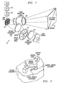
- FIG. 1 there is illustrated an overall block diagram of a digital micromirror device (DMD) display system.
- DMD digital micromirror device
- FIG. 1 an example of a DMD system 10 is illustrated, wherein the light from a light source 11 is applied through a first condenser lens 13 and through a color wheel 15, which is rotating at about sixty cycles or hertz or 60 frames per second.
- the light passing through the color wheel 15 passes through a second condenser lens 17 onto a DMD chip 19.
- the DMD chip includes an array of tiny mirror elements, or micromirrors, where each mirror element is hinged by torsion hinge and support post above a memory cell of a CMOS status RAM as shown in Fig. 2.
- the movable micromirror tilts into the on or off states by electrostatic forces based on data in the cell.
- the tilt of the mirror is either plus 10 degrees (on) or minus 10 degrees (off) to modulate the light that incident on the surface.
- the light reflected from any of the mirrors may pass through a projection lens 20 and create images on a large screen 21.
- the portion of time during which the video frame that a mirror remains in the on state determines the shade of grey.
- the time duration in which the cell is in the positive direction, or on, is represented by 8 bits of data sent to that cell.
- the color wheel 15 is divided into red, green, and blue sectors.
- the maximum red would when the red for example would be reflecting the maximum period of time as when the light is on the longest period of time in the red sector. The same would go for the other two colors.
- the minimum would be where the micromirror would not be reflecting through the color wheel and the lens, etc. at all during the color cycle.
- the intensity resolution in this pulse width modulation (PWM) is limited by the response time of the DMD mirrors.
- the total time available to display a color frame and the least time required to turn a mirror to the "on" state and back to "off” state defines the resolution of present systems.
- the most significant bit is the 7th bit with that bit representing the widest "on” time, the 6th bit being then the next widest "on” time, and the 5th bit representing the third longest “on” time, etc., all the way down to the least significant 0 bit, which is represented by the shortest time period.
- a sequential color DMD system might have 5 (five) msec (milliseconds) available for a color frame.
- the least significant bit (0 bit on only) the shortest period would be "on” for about 19.6 ⁇ s.
- the mirror on/off time would have to be less than 19.6 ⁇ s to implement this scheme with the current method.
- the DMD device In a system where the DMD device has the capability of only 6 bits, or even those that have the full eight bits, the system would have too few number of grades of grey or shades of color and therefore tend to show blockiness between portions of the picture. This would represent one of the errors that the present invention is to overcome.
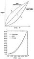
- FIG. 4a illustrates conventional degamma, SMPTE degamma, and Texas Instruments' degamma curves. This is done, for example, by each color providing the raster scanned gamma corrected red, green, or blue video data as shown in Fig. 1 using a gamma lookup table (LUT) 50 where for given input threshold levels the mirrors are turned on for given durations.
- LUT lookup table
- the output is stepped as shown in Fig. 5 rather than smooth between the thresholds of the bits and, therefore, the grade levels again take on a blockiness particularly in the low intensity regions.
- the problems of the low number of bits in the blockiness are solved by an error diffusion filter as shown in Fig. 6 for each color path (red, green, and blue) on the raster scanned video output that would normally be written into the frame RAM buffer 53.
- the filter 70 computes an error between the desired intensity of a pixel and the immediately lower achievable intensity of the DMD display. This error is then propagated into pixels to the right and below the first pixel as shown in Fig. 7.
- Fig. 6 An implementation of this filter for one color is illustrated in Fig. 6.
- the esired output for a given color is generated by a degamma lookup table (LUT) 50 at N bits of resolution and combined with errors for earlier pixels.
- the degamma LUT selected matches the appropriate curve in Fig. 4a.
- N is 12 bits addressed by 8-bits video data into the LUT 50.
- the M MSB (most significant bits) are then sent to the DMD frame buffer 53, and DMD display hardware while the N-M LSB (least significant bits) representing error are delayed for combination with later pixels.
- the error is distributed to the right and below using the four Isbs (least significant bits).
- the horizontal delay element 55 is implemented as a single N-M bit latch, while the vertical delay 57 is accomplished with an L word by N-M bit FIFO (first in first out) memory where L is the number of pixels in a video line. Both delay elements must have appropriate initialization circuitry.
- the vertical and horizontal error is divided by 2 at divider 59 and summed to the following row and column at summer 52. This filter may be accomplished with a video processor and with memory to accomplish the horizontal and vertical delays. As illustrated in Fig. 7, one-half of the error from the previous row (r-1) is provided to the row r and half of the error from the previous column (c-1) is provided to the next column (c). In this manner the error added enhances the apparent intensity resolution of the video display system.
- the FIFO memory for a video line described above can add a significant cost to the system, particularly when integrated with multiple functions in custom integrated circuits as might be desirable in high volume applications.
- only half of the pixels require half the storage that the filter mentioned above requires if the error terms least significant bits (lsbs) are shifted to the next video line from only half of the pixels.
- Fig. 8 One such filter design is illustrated in Fig. 8. The error terms from odd numbered pixel columns are shifted only horizontally, while errors from even columns shift to the next line.
- the FIFO vertical delay memory can be reduced to a length of half the number of pixels in a line.
- Fig. 9 illustrates a hardware block diagram for the filter to achieve the operation of Fig. 8.
- the pixel clock rate is divided by 2 so that every other error term is written into the vertical delay memory.
- the 12-bit output from the lookup table 51 is summed at summer 62 with the 4 least significant bits (Isbs) from the error diffusion.
- the 8 most significant bits (msb) are applied to the frame buffer.
- the lsbs (4 bits) are applied directly to multiplexer 67 and to delay 60, which are clocked by half the pixel rate by divider 61 to clockout from delay 60 the pixel data two pixels short of a full line delay.
- the output from delay 60 is applied to delay 63 and summer 65.
- Delay 63 is also clocked at the half pixel rate to add a two pixel delay to the output from delay 60.
- the output from each of the delays 60 and 63 is divided into half and applied to the other input of multiplexer 67, which alternately clocks the output from the two inputs at half the clock rate of the picture clock.
- the output from the multiplexer 67 is delayed one picture element at delay 69 that is clocked by the picture clock.
- the output from delay 69 is applied as 4 lsbs to summer 62.
- Another embodiment is illustrated in Fig. 10, wherein error added to a given or next pixel is from the error from the pixel delayed by one line delay and one pixel delay to the given pixel.
- the delays used are clocked at half the pixel clock rate to again reduce the size of the FIFO.
- a DMD display system includes an inverse gamma look-up-table (50) for converting raster scanned, gamma corrected video data of 8 bits to 12 bits inverse gamma data with 8 most significant bits (msb) and 4 least significant bits (lsb).
- the 8 msb are coupled to the micromirror of the DMD display (10) and the four lsb are delayed. For each input intensity in, the output intensity in will be displayed on the DMD device. If the degamma was perfect and there was no lack of bits, the value displayed in the DMD would be some other value N1.
- N1 was compute the difference between N and N1 and distribute this difference (error) among the neighboring pixels. The error can be distributed among the neighbors in various ways. One implementation is shown in Fig.
- a further advantage of the present invention is that the defect compensation can be performed as part of this algorithm.
- the DMD coordinates of defective pixels need to be known and the error diffusion needs to be modified to account for the fact that at those locations the pixel displays either bright (stuck ON), dark (stuck OFF) or neutral (flat pixel).
- the claimed filter is equally applicable to a three DMD system in place of the color wheeL
- the degamma lookup table may be different for the three primary colors.
Landscapes
- Engineering & Computer Science (AREA)
- Multimedia (AREA)
- Signal Processing (AREA)
- Theoretical Computer Science (AREA)
- Computer Hardware Design (AREA)
- General Physics & Mathematics (AREA)
- Physics & Mathematics (AREA)
- Chemical & Material Sciences (AREA)
- Crystallography & Structural Chemistry (AREA)
- Mechanical Light Control Or Optical Switches (AREA)
- Projection Apparatus (AREA)
- Control Of Indicators Other Than Cathode Ray Tubes (AREA)
- Transforming Electric Information Into Light Information (AREA)
Claims (4)
- Fehlerdiffusionsfilter (70) zum Verbessern der sichtbaren Intensitätsauflösung einer digitalen Mikrospiegelanzeigevorrichtung (19), die eine Matrix aus Mikrospiegeln umfasst und durch ein rasterabgetastetes Videosignal angesteuert wird, das mehrere Videozeilen (r - 1, r, r+1) repräsentiert, die ihrerseits mehrere Pixel repräsentieren, wobei das Filter umfasst:dadurch gekennzeichnet, dass die Fehlerwerte von jedem zweiten Pixel der momentanen Videozeile (r-1, r) innerhalb der Videozeile (r - 1, r) durch einen Horizontalverzögerungsspeicher (69) horizontal verschoben werden, während Fehlerwerte von den Pixeln zwischen jedem zweiten Pixel der Videozeile (r - 1, r) zu den Pixeln der nächsten Videozeile (r, r + 1) über den Vertikalverzögerungsspeicher (60, 63) verschoben werden.Mittel zum Bestimmen des Intensitätsfehlerwertes eines Pixels, der definiert ist als Differenz zwischen der gewünschten Intensität des Pixels, die entsprechend dem rasterabgetasteten Videosignal gegeben ist, und der nächstniedrigeren Intensität, die durch den dem gegebenen Pixel entsprechenden Mikrospiegel erzielbar ist, über den gesamten Intensitätsbereich; undMittel, die einen Vertikalverzögerungsspeicher (60, 63) enthalten, um die Intensitätsfehlerwerte zu den Pixeln der nächsten Videozeile (r, r+1) lediglich von einer Hälfte der Pixel der momentanen Videozeile (r - 1, r) weiterzutragen;
- Filter nach Anspruch 1, bei dem die Pixeltaktrate des Vertikalverzögerungsspeichers (60, 63) durch zwei geteilt ist, so dass jeder zweite Fehlerwert in dem Vertikalverzögerungsspeicher (60, 63) geschrieben wird.
- Digitales Anzeigesystem mit Mikrospiegelvorrichtungen, das umfasst:wobei das Fehlerdiffusionsfilter (70) zwischen die Nachschlagtabelle LUT (50) und die digitale Mikrospiegelvorrichtung (19) geschaltet ist, um Bits zu den Mikrospiegeln weiterzureichen, um die sichtbare Intensität zu erzielen, mit:ein Fehlerdiffusionsfilter (70) nach Anspruch 1 oder Anspruch 2;eine Lichtquelle (11);eine digitale Mikrospiegelvorrichtung (19), die eine Matrix aus Mikrospiegeln umfasst, die in Spalten und Zeilen angeordnet sind, die über einer entsprechenden Matrix von Halbleiterspeichervorrichtungen angebracht sind, wobei durch Operationen der Speichervorrichtungen die Mikrospiegel dazu veranlasst werden, Licht von der Lichtquelle (11) in einer gewünschten Richtung zu reflektieren, und die Dauer des reflektierten Lichts bei irgendeinem gegebenen Mikrospiegel die Pixelintensität von diesem Mikrospiegel ergibt;eine Quelle für eine erste Menge von Rasterabtastdaten zum Betreiben der Mikrospiegel unter Verwendung der Speichervorrichtungen für eine von den Daten abhängige Zeitdauer; undeine Degamma-Nachschlagtabelle LUT (50), die in Reaktion auf die Quelle für eine erste Menge von Rasterabtastdaten eine zweite Menge von Rasterabtastdaten bereitstellt, wobei die höchstwertigen Bits der zweiten Abtastdaten für jeden gegebenen Mikrospiegel die erreichbare Intensität repräsentieren, die der gewünschten Intensität bei dem gegebenen Mikrospiegel am nächsten kommt, ohne die gewünschte Intensität zu übersteigen, und wobei die niedrigstwertigen Bits der zweiten Abtastdaten für jeden gegebenen Mikrospiegel die Intensität repräsentieren, die zu benachbarten Mikrospiegeln addiert wird, um eine sichtbare Intensität bei dem gegebenen Mikrospiegel, die gleich der gewünschten Intensität ist, zu erzielen;Summationsmitteln (62), um die höchstwertigen Bits und verzögerte niedrigstwertige Bits von dem gegebenen Mikrospiegel zu summieren;Mitteln, um die höchstwertigen Bits von den Summationsmitteln (62) mit den Mikrospiegeln und die niedrigstwertigen Bits mit Verzögerungsmitteln (60, 63, 69) zu koppeln; undMitteln zum Koppeln des Ausgangs der Verzögerungsmittel (60, 63, 69) mit den Summationsmitteln (62), um die niedrigstwertigen Bits von den gegebenen Mikrospiegeln mit Mikrospiegeln, die zu dem gegebenen Mikrospiegel benachbart sind, zu koppeln; wobei die Verzögerungsmittel (60, 63, 69) die niedrigstwertigen Bits in der Weise verzögern, dass die niedrigstwertigen Bits zu den höchstwertigen Bits für die benachbarten Mikrospiegel addiert werden.
- Anzeigesystem mit digitalen Mikrospiegelvorrichtungen nach Anspruch 3, bei dem die vertikale Verzögerung (60, 63) ein FIFO-Speicher ist, dessen Länge gleich der halben Anzahl von Pixeln in einer Videozeile (r - 1, r, r + 1) ist.
Applications Claiming Priority (2)
| Application Number | Priority Date | Filing Date | Title |
|---|---|---|---|
| US315457 | 1994-09-30 | ||
| US08/315,457 US5726718A (en) | 1994-09-30 | 1994-09-30 | Error diffusion filter for DMD display |
Publications (3)
| Publication Number | Publication Date |
|---|---|
| EP0704835A2 EP0704835A2 (de) | 1996-04-03 |
| EP0704835A3 EP0704835A3 (de) | 1996-05-22 |
| EP0704835B1 true EP0704835B1 (de) | 2005-02-09 |
Family
ID=23224520
Family Applications (1)
| Application Number | Title | Priority Date | Filing Date |
|---|---|---|---|
| EP95114890A Expired - Lifetime EP0704835B1 (de) | 1994-09-30 | 1995-09-21 | Fehlerdiffusionsfilter für eine DMD-Anzeige |
Country Status (5)
| Country | Link |
|---|---|
| US (1) | US5726718A (de) |
| EP (1) | EP0704835B1 (de) |
| JP (1) | JPH08214244A (de) |
| KR (1) | KR100426917B1 (de) |
| DE (1) | DE69534001D1 (de) |
Families Citing this family (28)
| Publication number | Priority date | Publication date | Assignee | Title |
|---|---|---|---|---|
| US5592188A (en) | 1995-01-04 | 1997-01-07 | Texas Instruments Incorporated | Method and system for accentuating intense white display areas in sequential DMD video systems |
| JP4067594B2 (ja) | 1996-01-26 | 2008-03-26 | テキサス インスツルメンツ インコーポレイテツド | 信号変換回路および入力ワードのデジタル出力ワードへの変換方法 |
| US6342898B1 (en) * | 1998-03-16 | 2002-01-29 | Texas Instruments Incorporated | Compression and decompression of degamma tables for projection systems |
| US6271957B1 (en) * | 1998-05-29 | 2001-08-07 | Affymetrix, Inc. | Methods involving direct write optical lithography |
| US6657758B1 (en) | 1998-06-04 | 2003-12-02 | Board Of Regents, The University Of Texas System | Variable spectrum generator system |
| JP4016493B2 (ja) | 1998-08-05 | 2007-12-05 | 三菱電機株式会社 | ディスプレイ装置及びその多階調化回路 |
| US6583921B2 (en) * | 1999-12-28 | 2003-06-24 | Texas Instruments Incorporated | Micromechanical device and method for non-contacting edge-coupled operation |
| KR100371557B1 (ko) * | 2000-02-26 | 2003-02-14 | 조헌영 | 피혁분을 이용한 신발용 중창의 물성 개선 방법 |
| WO2001082281A1 (en) * | 2000-04-25 | 2001-11-01 | Koninklijke Philips Electronics N.V. | Method of reducing errors in displays using double-line sub-field addressing |
| JP4641334B2 (ja) * | 2000-07-18 | 2011-03-02 | キヤノン株式会社 | 画像表示装置 |
| JP5127089B2 (ja) | 2000-10-17 | 2013-01-23 | キヤノン株式会社 | 表示装置、投射型表示装置、光変調装置の駆動装置、及び光変調装置の駆動方法 |
| KR100434293B1 (ko) * | 2002-01-09 | 2004-06-05 | 엘지전자 주식회사 | 선형보간을 이용한 감마 보정 장치 |
| KR100434294B1 (ko) * | 2002-01-09 | 2004-06-05 | 엘지전자 주식회사 | 감마 보정 장치 |
| US7098927B2 (en) * | 2002-02-01 | 2006-08-29 | Sharp Laboratories Of America, Inc | Methods and systems for adaptive dither structures |
| US7295345B2 (en) * | 2003-04-29 | 2007-11-13 | Eastman Kodak Company | Method for calibration independent defect correction in an imaging system |
| CA2526467C (en) * | 2003-05-20 | 2015-03-03 | Kagutech Ltd. | Digital backplane recursive feedback control |
| US7701519B2 (en) * | 2003-06-19 | 2010-04-20 | Texas Instruments Incorporated | Display system and signal processing using diamond-shaped DMDs |
| KR100508936B1 (ko) * | 2003-08-12 | 2005-08-17 | 삼성에스디아이 주식회사 | 고속 동작이 가능한 오차 확산 방법 및 그 방법을 이용한플라즈마 디스플레이 패널 구동 장치 |
| US8243093B2 (en) | 2003-08-22 | 2012-08-14 | Sharp Laboratories Of America, Inc. | Systems and methods for dither structure creation and application for reducing the visibility of contouring artifacts in still and video images |
| US7164397B2 (en) * | 2003-09-30 | 2007-01-16 | Texas Instruments Incorporated | Discrete light color processor |
| US7352373B2 (en) * | 2003-09-30 | 2008-04-01 | Sharp Laboratories Of America, Inc. | Systems and methods for multi-dimensional dither structure creation and application |
| US7474316B2 (en) * | 2004-08-17 | 2009-01-06 | Sharp Laboratories Of America, Inc. | Bit-depth extension of digital displays via the use of models of the impulse response of the visual system |
| JP5586831B2 (ja) | 2004-11-10 | 2014-09-10 | トムソン ライセンシング | パルス幅変調(pwm)ディスプレイにおけるダークノイズ削減のためのシステムおよび方法 |
| US20060132471A1 (en) * | 2004-12-17 | 2006-06-22 | Paul Winer | Illumination modulation technique |
| JP2007101960A (ja) * | 2005-10-05 | 2007-04-19 | Fujitsu Hitachi Plasma Display Ltd | デジタル表示装置の表示方法及びデジタル表示装置 |
| FR2936817B1 (fr) * | 2008-10-07 | 2013-07-19 | Varel Europ | Procece pour fabriquer une piece comprenant un bloc en materiau dense du type carbure cemente, presentant un grandient de proprietes et piece obtenue |
| JP2012134912A (ja) * | 2010-12-24 | 2012-07-12 | Seiko Epson Corp | 画像処理装置、画像処理方法および画像処理プログラム |
| US20130135338A1 (en) * | 2011-11-30 | 2013-05-30 | Qualcomm Mems Technologies, Inc. | Method and system for subpixel-level image multitoning |
Family Cites Families (5)
| Publication number | Priority date | Publication date | Assignee | Title |
|---|---|---|---|---|
| JPS6163893A (ja) * | 1984-09-06 | 1986-04-02 | 株式会社日立製作所 | デイスプレイ装置における擬似中間調画像の表示方法 |
| US5201030A (en) * | 1989-09-28 | 1993-04-06 | Sun Microsystems, Inc. | Method and apparatus for dithering graphic images |
| GB9024978D0 (en) * | 1990-11-16 | 1991-01-02 | Rank Cintel Ltd | Digital mirror spatial light modulator |
| JPH0772824B2 (ja) * | 1991-12-03 | 1995-08-02 | インターナショナル・ビジネス・マシーンズ・コーポレイション | 表示システム |
| US5452024A (en) * | 1993-11-01 | 1995-09-19 | Texas Instruments Incorporated | DMD display system |
-
1994
- 1994-09-30 US US08/315,457 patent/US5726718A/en not_active Expired - Lifetime
-
1995
- 1995-09-21 EP EP95114890A patent/EP0704835B1/de not_active Expired - Lifetime
- 1995-09-21 DE DE69534001T patent/DE69534001D1/de not_active Expired - Lifetime
- 1995-09-29 KR KR1019950032772A patent/KR100426917B1/ko not_active Expired - Fee Related
- 1995-09-29 JP JP7253962A patent/JPH08214244A/ja active Pending
Non-Patent Citations (1)
| Title |
|---|
| IEEE SPECTRUM, vol. 30, no. 11, November 1993 (1993-11-01), pages 27 - 31 * |
Also Published As
| Publication number | Publication date |
|---|---|
| EP0704835A3 (de) | 1996-05-22 |
| DE69534001D1 (de) | 2005-03-17 |
| KR100426917B1 (ko) | 2004-06-16 |
| US5726718A (en) | 1998-03-10 |
| JPH08214244A (ja) | 1996-08-20 |
| EP0704835A2 (de) | 1996-04-03 |
| KR960011367A (ko) | 1996-04-20 |
Similar Documents
| Publication | Publication Date | Title |
|---|---|---|
| US5726718A (en) | Error diffusion filter for DMD display | |
| US5623281A (en) | Error diffusion filter for DMD display | |
| EP0823698B1 (de) | Verbesserungen an Anzeigesystemen mit digitaler Spiegelvorrichtung | |
| JP4215287B2 (ja) | 映像表示システムおよびそのアドレッシング方法 | |
| JP4077890B2 (ja) | イメージディスプレイシステムにおけるアーチファクト低減方法 | |
| KR100346877B1 (ko) | 디지탈비디오시스템에서순간아티팩트를감소시키는방법및시스템 | |
| EP1269756B1 (de) | Verbesserungen an dmd-bildanzeigevorrichtungen | |
| US6008785A (en) | Generating load/reset sequences for spatial light modulator | |
| US5497172A (en) | Pulse width modulation for spatial light modulator with split reset addressing | |
| CA2193422C (en) | Dmd-based projector for institutional use | |
| US8717394B2 (en) | Boundary dispersion for mitigating PWM temporal contouring artifacts in digital displays | |
| US20080279470A1 (en) | Motion Blur Reduction for Lcd Video/Graphics Processors | |
| US6226054B1 (en) | Global light boost for pulse width modulation display systems | |
| EP0755556B1 (de) | Verfahren und einrichtung zum steuern einer anzeigevorrichtung | |
| US7161608B2 (en) | Digital system and method for displaying images using shifted bit-weights for neutral density filtering applications | |
| US7471273B2 (en) | Bit segment timing organization providing flexible bit segment lengths | |
| US9344694B2 (en) | Spatial light modulator sub-pixel architecture and method | |
| EP0686954B1 (de) | Nicht binäres Pulseweitenmodulationsverfahren für räumliche Lichtmodulatoren | |
| EP0662774A1 (de) | Linearisierung für Videoanzeigesystem mit räumlichem Lichtmodulator | |
| US7403187B2 (en) | Generalized reset conflict resolution of load/reset sequences for spatial light modulators |
Legal Events
| Date | Code | Title | Description |
|---|---|---|---|
| PUAI | Public reference made under article 153(3) epc to a published international application that has entered the european phase |
Free format text: ORIGINAL CODE: 0009012 |
|
| AK | Designated contracting states |
Kind code of ref document: A2 Designated state(s): DE FR GB IT NL |
|
| PUAL | Search report despatched |
Free format text: ORIGINAL CODE: 0009013 |
|
| AK | Designated contracting states |
Kind code of ref document: A3 Designated state(s): DE FR GB IT NL |
|
| K1C1 | Correction of patent application (title page) published |
Effective date: 19960403 |
|
| 17P | Request for examination filed |
Effective date: 19961121 |
|
| 17Q | First examination report despatched |
Effective date: 20000324 |
|
| GRAP | Despatch of communication of intention to grant a patent |
Free format text: ORIGINAL CODE: EPIDOSNIGR1 |
|
| GRAS | Grant fee paid |
Free format text: ORIGINAL CODE: EPIDOSNIGR3 |
|
| GRAA | (expected) grant |
Free format text: ORIGINAL CODE: 0009210 |
|
| AK | Designated contracting states |
Kind code of ref document: B1 Designated state(s): DE FR GB IT NL |
|
| PG25 | Lapsed in a contracting state [announced via postgrant information from national office to epo] |
Ref country code: NL Free format text: LAPSE BECAUSE OF FAILURE TO SUBMIT A TRANSLATION OF THE DESCRIPTION OR TO PAY THE FEE WITHIN THE PRESCRIBED TIME-LIMIT Effective date: 20050209 Ref country code: IT Free format text: LAPSE BECAUSE OF FAILURE TO SUBMIT A TRANSLATION OF THE DESCRIPTION OR TO PAY THE FEE WITHIN THE PRESCRIBED TIME-LIMIT;WARNING: LAPSES OF ITALIAN PATENTS WITH EFFECTIVE DATE BEFORE 2007 MAY HAVE OCCURRED AT ANY TIME BEFORE 2007. THE CORRECT EFFECTIVE DATE MAY BE DIFFERENT FROM THE ONE RECORDED. Effective date: 20050209 Ref country code: FR Free format text: LAPSE BECAUSE OF NON-PAYMENT OF DUE FEES Effective date: 20050209 |
|
| REG | Reference to a national code |
Ref country code: GB Ref legal event code: FG4D |
|
| REF | Corresponds to: |
Ref document number: 69534001 Country of ref document: DE Date of ref document: 20050317 Kind code of ref document: P |
|
| PG25 | Lapsed in a contracting state [announced via postgrant information from national office to epo] |
Ref country code: DE Free format text: LAPSE BECAUSE OF FAILURE TO SUBMIT A TRANSLATION OF THE DESCRIPTION OR TO PAY THE FEE WITHIN THE PRESCRIBED TIME-LIMIT Effective date: 20050510 |
|
| NLV1 | Nl: lapsed or annulled due to failure to fulfill the requirements of art. 29p and 29m of the patents act | ||
| PLBE | No opposition filed within time limit |
Free format text: ORIGINAL CODE: 0009261 |
|
| STAA | Information on the status of an ep patent application or granted ep patent |
Free format text: STATUS: NO OPPOSITION FILED WITHIN TIME LIMIT |
|
| 26N | No opposition filed |
Effective date: 20051110 |
|
| EN | Fr: translation not filed | ||
| PGFP | Annual fee paid to national office [announced via postgrant information from national office to epo] |
Ref country code: GB Payment date: 20100809 Year of fee payment: 16 |
|
| GBPC | Gb: european patent ceased through non-payment of renewal fee |
Effective date: 20110921 |
|
| PG25 | Lapsed in a contracting state [announced via postgrant information from national office to epo] |
Ref country code: GB Free format text: LAPSE BECAUSE OF NON-PAYMENT OF DUE FEES Effective date: 20110921 |