EP0704849B1 - Semiconductor memory device with synchronous dram whose speed grade is not limited - Google Patents
Semiconductor memory device with synchronous dram whose speed grade is not limited Download PDFInfo
- Publication number
- EP0704849B1 EP0704849B1 EP95115250A EP95115250A EP0704849B1 EP 0704849 B1 EP0704849 B1 EP 0704849B1 EP 95115250 A EP95115250 A EP 95115250A EP 95115250 A EP95115250 A EP 95115250A EP 0704849 B1 EP0704849 B1 EP 0704849B1
- Authority
- EP
- European Patent Office
- Prior art keywords
- signal
- clock signal
- output
- data
- clock
- Prior art date
- Legal status (The legal status is an assumption and is not a legal conclusion. Google has not performed a legal analysis and makes no representation as to the accuracy of the status listed.)
- Expired - Lifetime
Links
Images


Classifications
-
- G—PHYSICS
- G11—INFORMATION STORAGE
- G11C—STATIC STORES
- G11C11/00—Digital stores characterised by the use of particular electric or magnetic storage elements; Storage elements therefor
- G11C11/21—Digital stores characterised by the use of particular electric or magnetic storage elements; Storage elements therefor using electric elements
- G11C11/34—Digital stores characterised by the use of particular electric or magnetic storage elements; Storage elements therefor using electric elements using semiconductor devices
- G11C11/40—Digital stores characterised by the use of particular electric or magnetic storage elements; Storage elements therefor using electric elements using semiconductor devices using transistors
- G11C11/401—Digital stores characterised by the use of particular electric or magnetic storage elements; Storage elements therefor using electric elements using semiconductor devices using transistors forming cells needing refreshing or charge regeneration, i.e. dynamic cells
- G11C11/4063—Auxiliary circuits, e.g. for addressing, decoding, driving, writing, sensing or timing
- G11C11/407—Auxiliary circuits, e.g. for addressing, decoding, driving, writing, sensing or timing for memory cells of the field-effect type
-
- G—PHYSICS
- G11—INFORMATION STORAGE
- G11C—STATIC STORES
- G11C7/00—Arrangements for writing information into, or reading information out from, a digital store
- G11C7/10—Input/output [I/O] data interface arrangements, e.g. I/O data control circuits, I/O data buffers
- G11C7/1072—Input/output [I/O] data interface arrangements, e.g. I/O data control circuits, I/O data buffers for memories with random access ports synchronised on clock signal pulse trains, e.g. synchronous memories, self timed memories
-
- G—PHYSICS
- G11—INFORMATION STORAGE
- G11C—STATIC STORES
- G11C7/00—Arrangements for writing information into, or reading information out from, a digital store
- G11C7/10—Input/output [I/O] data interface arrangements, e.g. I/O data control circuits, I/O data buffers
- G11C7/1015—Read-write modes for single port memories, i.e. having either a random port or a serial port
- G11C7/1039—Read-write modes for single port memories, i.e. having either a random port or a serial port using pipelining techniques, i.e. using latches between functional memory parts, e.g. row/column decoders, I/O buffers, sense amplifiers
Definitions
- This invention relates to semiconductor memory devices, and more particularly to semiconductor memory devices, in which the speed grade of synchronous DRAM, synchronous SRAM, etc. synchronized to an external clock is improved when the Column Address Strobe (CAS) latency is 2.
- CAS Column Address Strobe
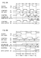
- Figs. 1A and 1B are timing charts of operation of the synchronous DRAM in the literature, Fig. 1A being for the case when the CAS latency is 3, and Fig. 1B being for the case when the CAS latency is 2.
- Fig. 1C is a timing chart of operation of a general purpose DRAM corresponding to the timing charts in Figs. 1A and 1B. Referring to Figs.
- external signals for instance, a command signal (COMMAND) and an external address signal (ADD) are latched in synchronism to the rise timing of a clock signal from low level to high level, the latched signals being decoded to be recognized as respective commands.
- a command signal for instance, a command signal (COMMAND) and an external address signal (ADD)
- ADD external address signal
- CAS latency refers to the necessary number of clock cycles from the designation of column address (READ command input) till the outputting of the designated address data.
- data of internal address signal A1 turns to be outputted as the first output data, and a memory system latches and outputs this data at the rise timing of clock cycle C7 delayed three clock cycles, thus providing CAS latency of 3.
- data of internal addresses A2 to A4 generated in an internal counter i.e., a burst counter
- a row address signal (ROW) and an active command (ACT) are supplied in synchronism to clock cycle C1 of the clock signal, corresponds in the general purpose DRAM to Row Address Strobe (RAS) inversion signal in clock cycle C1 from high level to low level, and a word line for taking out the low address signal is selected, thereby amplifying the memory cell data in a sense amplifier.
- RAS Row Address Strobe
- the supplying of the external address signal A1 and the READ command in synchronism to clock cycle C1 corresponds in the general purpose DRAM to the supplying of the external address signal A1 and the inverting of the CAS inversion signal from high level to low level in clock cycle C4, and data of address A1 is read out as shown in Fig. 1C.
- the supplying of a precharge command (PRE) in synchronism to clock cycle C13 corresponds, in the general purpose DRAM, to the inverting of the RAS inversion signal from low level to high level in clock cycle C13.
- PRE precharge command
- the speed grade which represents the typical operation speed of the current general purpose DRAM is -60.
- time from the external address signal input till the output of data stored in a memory cell from an output buffer, i.e., address access time is 30 nsec.
- address access time is 30 nsec.
- the internal operation from the supply of the READ command till the output of the memory cell data from the output buffer corresponds to the operation in the address access time of the general purpose DRAM.
- Fig. 2 is schematic representation of a prior art example of semiconductor memory device.
- This memory device adopts a three-stage pipeline system, in which the flow of signal from the supply of an external address signal till the memory data output from the output buffer, i.e., the address access bus, is divided by three latch circuits.
- This semiconductor memory device comprises an input buffer 1 for receiving an external address signal supplied from an input terminal 17; a burst counter 2 for latching the external address signal output in synchronism to a clock signal supplied from a terminal 18 through buffer 10, thus generating internal addresses A1, A2, A3, ..., a column decoder 3 including NAND gates 31a, 31b, ..., for decoding the data output of the burst counter 2; a column switch latch portion 4 including a plurality of latch elements each having a switch 41a and inverters 42a and 43a, for latching the column decoder output in synchronism to a control signal which is outputted from an OR gate 11 for taking logical sum (OR operation) of the clock signal and an internally supplied mode signal 19; a memory block 5; a column selector constituting the memory block 5 and including a series circuit having a transistor 51a with a column selection signal 23 coupled thereto and a transistor 52a with one sense amplifier output coupled thereto at the gate, and another series circuit having a transistor 51b with the
- the column decoder 3, column switch latch portion 4 and memory clock 5 are shown only partly for facilitating the description.
- a portion from the burst counter 2 to the column switch latch portion 4 is shown as a first stage 36 of pipeline, a portion from the column switch latch portion 4 to the output data latch circuit 8 is shown as a second stage 37 of pipeline, and a portion from the output data latch circuit 8 to the output terminal 20 is shown as a third stage 38 of pipeline.
- Figs. 3A and 3B are timing charts for describing the operation of the above Fig. 2 structure, Fig. 3A being for a case when the CAS latency is 3, and Fig. 5B being for a case when the CAS latency is 2.
- the burst counter 2 latches external address signal A1, and generates and outputs internal address signals A1, A2, A3, ... which are decoded in the column decoder 3.
- the output of the column decoder 3 is latched in synchronism to the clock signal on the control signal line 27, and by this latched output signal which is at high level, the transistors 51a and 51b of the memory block 5 are selected.
- the word line 29 that is selected by an active command and a row address (ROW) allows memory cell data to be read out onto the pair digit lines 30 and 31.
- the data thus read out is amplified in the sense amplifier 53 to render one of the pair digit lines 30 and 31 to be at high level and the other at low level.
- the transistor 52a is activated and then the transistors 51a and 51b are activated.
- the read bus 25 to which the activated transistor 51a is connected becomes low level.
- the read bus 26 to which the non-activated transistor 51b is connected becomes high level because it is pulled up to the power source potential VDD by the load element 34.
- the output latch circuit 8 latches data supplied in synchronism to the clock signal on the control signal line 28, and outputs the latched data to the outside through the output buffer 9.
- the mode signal 19 becomes high level to forcibly fix the output of the OR gate 11 to high level, and the second stage of pipeline is not latched but is brought to a state in which data is outputted by inversion only. That is, the first and second stages of pipeline are coupled together and operated in one clock cycle, thereby realizing the CAS latency of 2.
- the signal processing times or capacities of the first stage, the second stage and the third stage of pipeline are about 7, 10 and 10 nsec., respectively.
- the minimum clock cycle that is necessary for obtaining the operation of all the pipeline stages is 10 nsec., that is, the corresponding maximum frequency is 100 MHz.
- the first and second stages of pipeline are coupled together for one clock cycle operation.
- the time from the inputting of the external address signal till the outputting of data stored in the memory cell from the output buffer i.e., the address access time
- the internal operation of the synchronous DRAM from the supplying of the READ command till the outputting of the memory cell data from the output buffer corresponds to the operation of the general purpose DRAM in the address access time thereof.
- the CAS latency of 2 determines the upper limit of the speed grade, resulting in an operation speed deterioration as great as about 15%, and therefore it is impossible to attain the desired speed grade.
- An object of the present invention which has been intended in view of the above drawbacks inherent in the prior art, is to provide a synchronous DRAM, which can improve the operation speed upper limit in a case when the CAS latency is 2.
- Fig. 4 is a schematic representation of an embodiment of the semiconductor memory device according to the invention. This embodiment is different from the prior art example described above in that, when the CAS latency is 2, the output data latch control signal supply timing is delayed by a delay circuit to provide the same speed grade as in the case of the general purpose DRAM.
- an external address signal input terminal 17 is connected to an input buffer 1, which has its output terminal connected to a data input terminal of a burst counter 2.
- a control signal input terminal of the burst counter 2 is connected to a control line 21, to which a clock signal is supplied from an input terminal 18 through a buffer 10.
- a data output terminal of the burst counter 2 is connected via an internal address signal line 22 to input terminals of NAND gates 31a and 31b of a column decoder 3.
- Output terminals of the column decoder 3 are connected to a data input terminal of a switch 41a of a column switch latch portion 4.
- To a control signal input terminal of the column switch latch portion 4 is connected via a control signal line 27 the output of an OR gate 11 for taking logical sum of an internally supplied mode signal 19 and the clock signal supplied from the terminal 18.
- the column switch latch portion 4 includes a predetermined number of latch circuits each of which has a switch 41a having a control signal input terminal, an inverter 42a, the switch 41a and inverter 42a being cascade connected between the data input terminal and a data output terminal, and an inverter 43a in parallel with and in the inverse polarity to the inverter 42a.
- An output terminal of the column switch latch portion 4 is connected via a column selection signal line 23 to the gates of transistors 51a and 51b of a memory block 5.
- the memory block 5 includes transistors 51a and 52a connected in series between a read bus 25 and ground potential and transistors 51b and 52b connected in series between a read bus 26 and ground potential.
- a sense amplifier 53 has a pair of output terminals that are connected to the gates of the respective transistors 52a and 52b.
- a pair of input terminals of the sense amplifier 53 are connected to a pair of digit lines 30 and 31.
- a cell 54 is disposed at an intersection of word line 29 crossing the pair of digit lines 30 and 31.
- the read buses 25 and 26 are pulled up by respective load elements 34 and 35 to the power supply voltage VDD and connected to a data amplifier 6.
- An output terminal of the data amplifier 6 is connected via read/write buses 32 and 33 to a data input terminal of a data amplifier 7, which has its output line connected to a data input terminal of an output data latch circuit 8.
- an output terminal of an OR gate 16 for taking logical sum of the output of an AND gate 14, which has an input terminal connected through a delay circuit 13 to the clock signal input terminal 19 and the other input terminal connected to a mode signal input terminal, and the output of an AND gate 15, which has an input terminal connected to the clock signal input terminal 18 and the other input terminal connected through an inverter 12 to a signal line of mode signal 19.
- the output data latch circuit 8 has an output line connected through a buffer 9 to a data output terminal 20.
- the column decoder 3, column switch latch portion 4 and memory block 5 are shown only partly for facilitating the description.
- a portion from the burst counter 2 to the column switch latch portion 4 is shown as a first stage 36 of pipeline, a portion from the column switch latch portion 4 to the output data latch circuit 8 is shown as a second stage 37 of pipeline, and a portion from the output data latch circuit 8 to the output terminal 20 is shown as a third stage 38 of pipeline.
- Figs. 5A and 5B are timing charts for describing the operation of the above Fig. 4 structure, Fig. 5A being for a case when the CAS latency is 3, and Fig. 5B being a case when the CAS latency is 2.
- the burst counter 2 latches external address signal A1, and generates and outputs internal address signals A1, A2, A3, ..., these address signals being decoded in a column decoder 3 and then supplied to the column switch latch portion 4.
- the OR gate 11 When the CAS latency is 3, with the mode signal set to low level, the OR gate 11 outputs the supplied clock signal directly to a control signal line 27.
- the column switch latch portion 4 latches the output of the column decoder 3 in synchronism to the clock signal, and by this latched output signal which is at a high level, the transistors 51a and 51b of the memory block 5 are selected.
- data in the memory cell 54 is read out via a word line 29 which is selected according to an active command and a row address (ROW) (both being not shown) to the pair digit lines 30 and 31.
- This read-out memory cell data is amplified by the sense amplifier 53 to render one of the pair of digit lines 30 and 31 to high level and the other to low level.
- the transistor 52a for instance, is activated, and then the transistors 51a and 51b are activated by column selection signal 23 outputted from the column switch latch portion 4, and thus the read bus 25 with the transistor 51a connected thereto becomes low level.
- the transistor 52b connected to the bit line 31 of low level is not activated, and thus the read bus 26 with the transistor 51b connected thereto becomes high level since the read bus has been pulled up by the load element 35 to the power supply potential VDD.
- the cell data read out to the read buses 25 and 26 are amplified by the data amplifiers 6 and 7, and then supplied to the output latch circuit 8.
- the mode signal 19 is at low level
- the high level output of the inverter 12 is supplied to one input terminal of the AND gate 15, and thus the clock signal supplied to the other input terminal is directly outputted to one input terminal of the OR gate 16.
- the output of the AND gate 14 is fixed to low level and, thus, the OR gate 16 transfers the clock signal to the control signal line 28.
- the output latch circuit 8 latches the supplied cell data and begins to output data through the output buffer 9 and data output terminal 20 to the outside.
- the first and second stages of pipeline are coupled together for one clock cycle operation thereof, whereby, when the CAS latency is 2, the first and second stages of pipeline are operated in clock cycle C1, and thus up to the end timing of the clock cycle C1, the transistors 51a and 51b are selected to specify memory cell, data therein being thus amplified in the sense amplifier 53, and the amplified data is outputted to the read buses 25 and 26.
- the data is further amplified in the data amplifiers 6 and 7 and then supplied to the output data latch circuit 8.
- the inverter since the mode signal 19 is at high level, the inverter provides a low level output to one input terminal of the AND gate 15. Since this signal is not influenced by the clock signal supplied to the other input terminal, the output of the AND gate 15 is fixed to low level so that the input to one input terminal of the OR gate 16 is fixed in level.
- the output of the AND gate 14 is supplied to the other input terminal of the OR gate 16.
- one input terminal of the AND gate 14 is fixed to high level of the mode signal 19, while clock signal which has been delayed in the delay circuit 13 by a predetermined delay time, for instance a design delay time of 4 nsec., is supplied to the other input terminal, this clock signal delayed by 4 nsec. being supplied directly to the output terminal of the AND gate 14.
- the OR gate 16 transfers the delayed clock signal mentioned above to the control signal line 28.
- the output latch circuit 8 latches the supplied cell data in synchronism to the delayed clock signal, and begins to output the latched data through the output buffer 9 and the data output terminal 20 to the outside.
- the delay time of 4 nsec. means that the clock signal is designed such that the virtual operation speed is 13 and 14 nsec. in the first and second cycles, respectively.
- the operation speed capacity of the synchronous DRAM is, as mentioned above, 7, 10 and 10 nsec. in the first to third stages of pipeline, respectively, so that the sum of the clock cycles C1 and C2 of the clock signal 18 in Fig. 5B is 27 nsec. Where the first and second stages are directly coupled together, the clock cycle is 17 nsec.
- the maximum frequency is 71 MHz, and no restriction is imposed on the upper limit of the speed grade that may otherwise result from setting the CAS latency to 2, so that it is possible to achieve a speed grade of -10.
- the invention is applicable as well to, for instance, a synchronous DRAM of a two-bit pre-fetch system.
- the invention is applicable not only to the synchronous DRAM but also to a semiconductor memory device operable in synchronism to a clock, for instance a synchronous SRAM.
Landscapes
- Engineering & Computer Science (AREA)
- Microelectronics & Electronic Packaging (AREA)
- Computer Hardware Design (AREA)
- Dram (AREA)
- Static Random-Access Memory (AREA)
Applications Claiming Priority (3)
| Application Number | Priority Date | Filing Date | Title |
|---|---|---|---|
| JP23273094 | 1994-09-28 | ||
| JP232730/94 | 1994-09-28 | ||
| JP6232730A JP2616567B2 (ja) | 1994-09-28 | 1994-09-28 | 半導体記憶装置 |
Publications (3)
| Publication Number | Publication Date |
|---|---|
| EP0704849A2 EP0704849A2 (en) | 1996-04-03 |
| EP0704849A3 EP0704849A3 (en) | 1997-08-27 |
| EP0704849B1 true EP0704849B1 (en) | 2001-12-05 |
Family
ID=16943890
Family Applications (1)
| Application Number | Title | Priority Date | Filing Date |
|---|---|---|---|
| EP95115250A Expired - Lifetime EP0704849B1 (en) | 1994-09-28 | 1995-09-27 | Semiconductor memory device with synchronous dram whose speed grade is not limited |
Country Status (5)
| Country | Link |
|---|---|
| US (1) | US5550784A (ja) |
| EP (1) | EP0704849B1 (ja) |
| JP (1) | JP2616567B2 (ja) |
| KR (1) | KR0166000B1 (ja) |
| DE (1) | DE69524348T2 (ja) |
Families Citing this family (23)
| Publication number | Priority date | Publication date | Assignee | Title |
|---|---|---|---|---|
| JPH0855471A (ja) * | 1994-08-12 | 1996-02-27 | Nec Corp | 同期型半導体記憶装置 |
| JPH08195077A (ja) * | 1995-01-17 | 1996-07-30 | Internatl Business Mach Corp <Ibm> | Dramの転送方式 |
| JP2658958B2 (ja) * | 1995-03-31 | 1997-09-30 | 日本電気株式会社 | Dmaコントローラ |
| JPH0934827A (ja) * | 1995-07-14 | 1997-02-07 | Canon Inc | メモリ制御装置 |
| JP2746222B2 (ja) * | 1995-08-31 | 1998-05-06 | 日本電気株式会社 | 半導体記憶装置 |
| JP3351692B2 (ja) * | 1995-09-12 | 2002-12-03 | 株式会社東芝 | シンクロナス半導体メモリ装置 |
| JP2991094B2 (ja) * | 1995-09-19 | 1999-12-20 | 日本電気株式会社 | 半導体記憶装置 |
| US5925142A (en) * | 1995-10-06 | 1999-07-20 | Micron Technology, Inc. | Self-test RAM using external synchronous clock |
| KR0157289B1 (ko) * | 1995-11-13 | 1998-12-01 | 김광호 | 컬럼 선택 신호 제어회로 |
| KR100375597B1 (ko) * | 1996-06-29 | 2003-05-09 | 주식회사 하이닉스반도체 | 버스트 카운터 불안정화 방지장치 |
| JP3305975B2 (ja) * | 1997-03-06 | 2002-07-24 | 株式会社東芝 | アドレスカウンタ回路及び半導体メモリ装置 |
| JPH113588A (ja) * | 1997-06-12 | 1999-01-06 | Nec Corp | 半導体記憶装置 |
| KR100492991B1 (ko) * | 1997-11-03 | 2006-04-28 | 삼성전자주식회사 | 버스트카운터및이를이용한싱크로너스디램 |
| DE69923769T2 (de) * | 1998-04-01 | 2006-02-02 | Mosaid Technologies Incorporated, Kanata | Asynchrones halbleiterspeicher-fliessband |
| CA2233789C (en) | 1998-04-01 | 2013-06-11 | Ian Mes | Semiconductor memory asynchronous pipeline |
| US6049505A (en) | 1998-05-22 | 2000-04-11 | Micron Technology, Inc. | Method and apparatus for generating memory addresses for testing memory devices |
| JP4034886B2 (ja) * | 1998-10-13 | 2008-01-16 | 富士通株式会社 | 半導体装置 |
| KR100304705B1 (ko) * | 1999-03-03 | 2001-10-29 | 윤종용 | 포스티드 카스 레이턴시 기능을 가지는 동기식 반도체 메모리 장치 및 카스 레이턴시 제어 방법 |
| KR100341587B1 (ko) * | 1999-11-12 | 2002-06-22 | 박종섭 | 리드 레이턴시와 동일한 라이트 레이턴시를 갖는 동기식디램 |
| JP4253097B2 (ja) | 1999-12-28 | 2009-04-08 | 東芝マイクロエレクトロニクス株式会社 | 半導体記憶装置及びそのデータ読み出し方法 |
| KR100314807B1 (ko) * | 1999-12-28 | 2001-11-17 | 박종섭 | 반도체메모리 장치의 파이프 제어 장치 |
| JP2004502267A (ja) | 2000-07-07 | 2004-01-22 | モサイド・テクノロジーズ・インコーポレイテッド | アクセス待ち時間が均一な高速dramアーキテクチャ |
| US7184328B2 (en) * | 2004-10-18 | 2007-02-27 | Infineon Technologies Ag | DQS for data from a memory array |
Family Cites Families (5)
| Publication number | Priority date | Publication date | Assignee | Title |
|---|---|---|---|---|
| KR950010564B1 (en) * | 1992-10-02 | 1995-09-19 | Samsung Electronics Co Ltd | Data output buffer of synchronous semiconductor memory device |
| US5454097A (en) * | 1993-01-25 | 1995-09-26 | Motorola, Inc. | Cascadable peripheral data interface including a shift register, counter, and randomly-accessed registers of different bit length |
| JPH0765577A (ja) * | 1993-08-30 | 1995-03-10 | Oki Electric Ind Co Ltd | 半導体記憶装置の出力回路 |
| US5430680A (en) * | 1993-10-12 | 1995-07-04 | United Memories, Inc. | DRAM having self-timed burst refresh mode |
| EP0660329B1 (en) * | 1993-12-16 | 2003-04-09 | Mosaid Technologies Incorporated | Variable latency, output buffer and synchronizer for synchronous memory |
-
1994
- 1994-09-28 JP JP6232730A patent/JP2616567B2/ja not_active Expired - Fee Related
-
1995
- 1995-09-26 US US08/534,270 patent/US5550784A/en not_active Expired - Lifetime
- 1995-09-27 KR KR1019950032081A patent/KR0166000B1/ko not_active Expired - Fee Related
- 1995-09-27 EP EP95115250A patent/EP0704849B1/en not_active Expired - Lifetime
- 1995-09-27 DE DE69524348T patent/DE69524348T2/de not_active Expired - Fee Related
Also Published As
| Publication number | Publication date |
|---|---|
| EP0704849A2 (en) | 1996-04-03 |
| EP0704849A3 (en) | 1997-08-27 |
| KR960012021A (ko) | 1996-04-20 |
| JP2616567B2 (ja) | 1997-06-04 |
| US5550784A (en) | 1996-08-27 |
| KR0166000B1 (ko) | 1999-02-01 |
| JPH0896574A (ja) | 1996-04-12 |
| DE69524348T2 (de) | 2002-08-22 |
| DE69524348D1 (de) | 2002-01-17 |
Similar Documents
| Publication | Publication Date | Title |
|---|---|---|
| EP0704849B1 (en) | Semiconductor memory device with synchronous dram whose speed grade is not limited | |
| US5537354A (en) | Semiconductor memory device and method of forming the same | |
| KR100202777B1 (ko) | 램의 컬럼액세스를 가속하기위한 데이타버스구조 | |
| US5581512A (en) | Synchronized semiconductor memory | |
| US6260128B1 (en) | Semiconductor memory device which operates in synchronism with a clock signal | |
| US5982674A (en) | Bi-directional data bus scheme with optimized read and write characters | |
| US6445632B2 (en) | Semiconductor memory device for fast access | |
| US6122220A (en) | Circuits and methods for generating internal signals for integrated circuits by dynamic inversion and resetting | |
| JP2907074B2 (ja) | 半導体記憶装置 | |
| JP3259764B2 (ja) | 半導体記憶装置 | |
| JP3846764B2 (ja) | 同期式半導体メモリ装置及びそのデータ入出力線のプリチャージ方法 | |
| US6073219A (en) | Semiconductor memory device with high speed read-modify-write function | |
| US6201756B1 (en) | Semiconductor memory device and write data masking method thereof | |
| US20020054515A1 (en) | Semiconductor memory device having row buffers | |
| US6166970A (en) | Priority determining apparatus using the least significant bit and CAS latency signal in DDR SDRAM device | |
| US6215837B1 (en) | Pipe counter signal generator processing double data in semiconductor device | |
| US7154316B2 (en) | Circuit for controlling pulse width | |
| JP2837127B2 (ja) | デュアルポートメモリ装置及びそのシリアルデータ出力方法 | |
| US20020085427A1 (en) | Semiconductor memory device for variably controlling drivability | |
| EP0714100B1 (en) | Synchronous memory device | |
| JPH0745067A (ja) | 半導体記憶装置 | |
| US5654934A (en) | Semiconductor memory employing a block-write system | |
| US6243302B1 (en) | Apparatus for outputting data using common pull-up/pull-down lines with reduced load | |
| US6026496A (en) | Method and apparatus for generating a pulse | |
| JPH04265598A (ja) | 半導体メモリ装置 |
Legal Events
| Date | Code | Title | Description |
|---|---|---|---|
| PUAI | Public reference made under article 153(3) epc to a published international application that has entered the european phase |
Free format text: ORIGINAL CODE: 0009012 |
|
| AK | Designated contracting states |
Kind code of ref document: A2 Designated state(s): DE FR GB |
|
| PUAL | Search report despatched |
Free format text: ORIGINAL CODE: 0009013 |
|
| AK | Designated contracting states |
Kind code of ref document: A3 Designated state(s): DE FR GB |
|
| 17P | Request for examination filed |
Effective date: 19970715 |
|
| 17Q | First examination report despatched |
Effective date: 19991018 |
|
| GRAG | Despatch of communication of intention to grant |
Free format text: ORIGINAL CODE: EPIDOS AGRA |
|
| GRAG | Despatch of communication of intention to grant |
Free format text: ORIGINAL CODE: EPIDOS AGRA |
|
| GRAH | Despatch of communication of intention to grant a patent |
Free format text: ORIGINAL CODE: EPIDOS IGRA |
|
| GRAH | Despatch of communication of intention to grant a patent |
Free format text: ORIGINAL CODE: EPIDOS IGRA |
|
| GRAA | (expected) grant |
Free format text: ORIGINAL CODE: 0009210 |
|
| AK | Designated contracting states |
Kind code of ref document: B1 Designated state(s): DE FR GB |
|
| REG | Reference to a national code |
Ref country code: GB Ref legal event code: IF02 |
|
| REF | Corresponds to: |
Ref document number: 69524348 Country of ref document: DE Date of ref document: 20020117 |
|
| PLBE | No opposition filed within time limit |
Free format text: ORIGINAL CODE: 0009261 |
|
| STAA | Information on the status of an ep patent application or granted ep patent |
Free format text: STATUS: NO OPPOSITION FILED WITHIN TIME LIMIT |
|
| 26N | No opposition filed | ||
| REG | Reference to a national code |
Ref country code: GB Ref legal event code: 732E |
|
| REG | Reference to a national code |
Ref country code: FR Ref legal event code: TQ |
|
| REG | Reference to a national code |
Ref country code: GB Ref legal event code: 732E |
|
| REG | Reference to a national code |
Ref country code: FR Ref legal event code: TP |
|
| PGFP | Annual fee paid to national office [announced via postgrant information from national office to epo] |
Ref country code: FR Payment date: 20080915 Year of fee payment: 14 |
|
| PGFP | Annual fee paid to national office [announced via postgrant information from national office to epo] |
Ref country code: DE Payment date: 20081002 Year of fee payment: 14 |
|
| PGFP | Annual fee paid to national office [announced via postgrant information from national office to epo] |
Ref country code: GB Payment date: 20081001 Year of fee payment: 14 |
|
| GBPC | Gb: european patent ceased through non-payment of renewal fee |
Effective date: 20090927 |
|
| REG | Reference to a national code |
Ref country code: FR Ref legal event code: ST Effective date: 20100531 |
|
| PG25 | Lapsed in a contracting state [announced via postgrant information from national office to epo] |
Ref country code: FR Free format text: LAPSE BECAUSE OF NON-PAYMENT OF DUE FEES Effective date: 20090930 Ref country code: DE Free format text: LAPSE BECAUSE OF NON-PAYMENT OF DUE FEES Effective date: 20100401 |
|
| PG25 | Lapsed in a contracting state [announced via postgrant information from national office to epo] |
Ref country code: GB Free format text: LAPSE BECAUSE OF NON-PAYMENT OF DUE FEES Effective date: 20090927 |