EP0704869A1 - Mehrfach-Durchführungskondensator - Google Patents
Mehrfach-Durchführungskondensator Download PDFInfo
- Publication number
- EP0704869A1 EP0704869A1 EP95114753A EP95114753A EP0704869A1 EP 0704869 A1 EP0704869 A1 EP 0704869A1 EP 95114753 A EP95114753 A EP 95114753A EP 95114753 A EP95114753 A EP 95114753A EP 0704869 A1 EP0704869 A1 EP 0704869A1
- Authority
- EP
- European Patent Office
- Prior art keywords
- capacitor
- conductor
- capacitors
- concentrically
- multiple feed
- Prior art date
- Legal status (The legal status is an assumption and is not a legal conclusion. Google has not performed a legal analysis and makes no representation as to the accuracy of the status listed.)
- Granted
Links
- 239000003990 capacitor Substances 0.000 title claims abstract description 67
- 239000004020 conductor Substances 0.000 claims abstract description 24
- 238000004804 winding Methods 0.000 claims abstract 2
- 239000011248 coating agent Substances 0.000 claims description 6
- 238000000576 coating method Methods 0.000 claims description 6
- 230000001681 protective effect Effects 0.000 claims description 5
- 229910000859 α-Fe Inorganic materials 0.000 claims description 4
- 238000004519 manufacturing process Methods 0.000 description 5
- 238000011161 development Methods 0.000 description 1
- 230000018109 developmental process Effects 0.000 description 1
Images
Classifications
-
- H—ELECTRICITY
- H01—ELECTRIC ELEMENTS
- H01G—CAPACITORS; CAPACITORS, RECTIFIERS, DETECTORS, SWITCHING DEVICES, LIGHT-SENSITIVE OR TEMPERATURE-SENSITIVE DEVICES OF THE ELECTROLYTIC TYPE
- H01G4/00—Fixed capacitors; Processes of their manufacture
- H01G4/35—Feed-through capacitors or anti-noise capacitors
Definitions
- the invention relates to a multiple feed-through capacitor for lines with an N conductor and n (n ⁇ 1) phase conductors for EMC and protective filters for use in shielded rooms, systems and systems, which is built HF-tight in a metallic housing and at least each have an X and Y capacitor, which are designed as wound capacitors and have end contact layers on their end faces.
- the object of the present invention is to provide a multiple feedthrough capacitor of the type mentioned at the outset, which is distinguished by a reduced volume.
- an X capacitor is arranged with one end face for each phase conductor on one end face of the Y capacitor, that the face ends of the X and Y capacitors which are arranged with respect to one another are large and concentric are connected to each other that the N-conductor is connected to these end faces over a large area is that the N-conductor is passed through the center of the Y-capacitor, that the respective phase conductor is guided through a core hole of the X-capacitor and is largely and concentrically connected to the front contact layer of the X-capacitor on the phase coating side, and that the ground (PE) coating side of the Y capacitor is connected to the housing over a large area and concentrically.
- PE ground
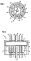
- FIG. 1 shows a multiple feedthrough capacitor 1 in a view from the N side. It consists of a Y capacitor 2 on one end face of which nine X capacitors 4 are fastened by connecting their end faces provided with Schoop layers over a large area and concentrically to the end face 3 of the Y capacitor, which is also provided with a Schoop layer.
- the end face 3 is the N coating of the Y capacitor 2 and represents the N potential of the multiple feedthrough capacitor 1.
- the N conductor N is likewise connected to the end face 3 over a large area and is carried out through the free space of the X capacitors.
- the nine phase conductors L1 ?? L9 are led through the core hole of the X capacitors 4 and are connected to the corresponding Schoop layers over a large area and concentrically on the phase coating side.
- the front contact layer 5 of the Y capacitor forms the PE (ground) potential and is connected over a large area and concentrically to the HF-tight housing 6.
- the end faces 7 of the X capacitors 4 represent their phase coating sides.
- Ferrite cores can optionally be applied to the conductors N, L1 ??. L9, so that a multiple feedthrough filter is obtained.
- the multiple feedthrough capacitor 1 shown is constructed as an n-fold feedthrough capacitor and is extremely low leakage current. It has an enclosing RF-tight envelope (housing 6) together for the Y capacitor 2 and all X capacitors 4, the electrical potential of this envelope being equal to the ground (PE) potential.
- PE ground
- the currents can be almost tripled by connecting the X capacitors 4 [eg (L1, L4, L7) + (L2, L5, L8) + (L3, L6, L9)] in parallel.
- Other versions are also possible to raise the listed combination, [eg combination as 2- + 4- + 3-wire etc.] or as a three-phase and direct current version.
- control line feed-through capacitors (nine pieces in the embodiment according to FIGS. 1 and 2) by connecting the N and the respective PE conductors, which, however, are not low in leakage current.
Landscapes
- Engineering & Computer Science (AREA)
- Power Engineering (AREA)
- Manufacturing & Machinery (AREA)
- Microelectronics & Electronic Packaging (AREA)
- Fixed Capacitors And Capacitor Manufacturing Machines (AREA)
- Filters And Equalizers (AREA)
- Shielding Devices Or Components To Electric Or Magnetic Fields (AREA)
Abstract
Description
- Die Erfindung betrifft einen Mehrfach-Durchführungskondensator für Leitungen mit einem N-Leiter und n (n≧1) Phasenleitern für EMV- und Schutzfilter zum Einsatz bei geschirmten Räumen, Systemen und Anlagen, der HF-dicht in ein metallisches Gehäuse eingebaut ist und aus zumindest jeweils einem X- und Y-Kondensator besteht, die als Wickelkondensatoren ausgebildet sind und an ihren Stirnseiten Stirnkontaktschichten aufweisen.
- Um hochwertige Schutzfilter (Schutzeinheiten) für geschirmte Räume, Systeme und Anlagen für Frequenzen ab einigen MHz bis zu mehreren GHz herzustellen, werden Mehrfach-Durchführungskondensatoren bzw. Mehrfach-Durchführungsfilter benötigt. Bisher gibt es für diese spezielle Anwendung keine Sonderkondensatoren, so daß eine sehr komplizierte Fertigung für beispielsweise einen 4-fach-Durchführungskondensator notwendig ist. Aufgrund dieser speziellen Fertigung ist das Volumen dieser Mehrfach-Durchführungskondensatoren wegen der sehr großen räumlichen Abmessungen relativ groß, woraus hohe Fertigungskosten resultieren.
- Aufgabe der vorliegenden Erfindung ist es, einen Mehrfach-Durchführungskondensator der eingangs genannten Art anzugeben, der sich durch ein verringertes Volumen auszeichnet.
- Diese Aufgabe wird erfindungsgemäß dadurch gelöst, daß beim eingangs angeführten Mehrfach-Durchführungskondensator an einer Stirnseite des Y-Kondensators für jeden Phasenleiter ein X-Kondensator mit seiner einen Stirnseite angeordnet ist, daß die zueinander angeordneten Stirnseiten der X- und Y-Kondensatoren großflächig und konzentrisch miteinander verbunden sind, daß an diesen Stirnseiten der N-Leiter großflächig angeschlossen ist, daß der N-Leiter durch die Mitte des Y-Kondensators durchgeführt ist, daß der jeweilige Phasenleiter durch ein Kernloch des X-Kondensators geführt und auf der Phasenbelagsseite großflächig und konzentrisch mit der Stirnkontaktschicht des X-Kondensators verbunden ist, und daß die Masse(PE)-Belagsseite des Y-Kondensators großflächig und konzentrisch mit dem Gehäuse verbunden ist.
- Weiterbildungen der Erfindung bestehen darin, daß die X-Kondensatoren symmetrisch am Y-Kondensator angeordnet sind und daß gegebenenfalls auf die Phasenleiter Ferritkerne aufgeschoben sind.
- Die Erfindung wird anhand der folgenden Ausführungsbeispiele erläutert.
- In der dazugehörenden Zeichnung zeigen:
- Fig.1 einen Mehrfach-Durchführungskondensator in Draufsicht,
- Fig.2 eine Seitenansicht des in Fig.1 gezeigten Kondensators.
- In der Fig.1 ist ein Mehrfach-Durchführungskondensator 1 in Ansicht von der N-Seite dargestellt. Er besteht aus einem Y-Kondensator 2 an dessen einer Stirnseite neun X-Kondensatoren 4 befestigt sind, indem ihre mit Schoopschichten versehenen Stirnseiten großflächig und konzentrisch mit der ebenfalls mit einer Schoopschicht versehenen Stirnseite 3 des Y-Kondensators verbunden werden. Die Stirnseite 3 ist der N-Belag des Y-Kondensators 2 und stellt das N-Potential des Mehrfach-Durchführungskondensators 1 dar. Der N-Leiter N wird ebenfalls großflächig mit der Stirnseite 3 verbunden und durch den freien Raum der X-Kondensatoren durchgeführt. Die neun Phasenleiter L1......L9 werden durch das Kernloch der X-Kondensatoren 4 geführt und auf der Phasenbelagsseite großflächig und konzentrisch mit den entsprechenden Schoopschichten verbunden.
- In Fig.2 ist der Mehrfach-Durchführungskondensator in Seitenansicht dargestellt. Die Stirnkontaktschicht 5 des Y-Kondensators bildet das PE(Masse)-Potential und ist großflächig und konzentrisch mit dem HF-dicht umschließenden Gehäuse 6 verbunden. Die Stirnflächen 7 der X-Kondensatoren 4 stellen ihre Phasenbelagsseiten dar.
- Auf die Leiter N,L1.......L9 können gegebenfalls Ferritkerne aufgebracht werden, so daß ein Mehrfach-Durchführungsfilter erhalten wird.
- Durch die in den Ausführungsbeispielen beschriebene Lösung ist es möglich, EMV- und Schutzfilter in kompakter Bauform wirtschaftlich herzustellen. Auch können Systeme und Anlagen EMV-technisch behandelt werden.
- Der dargestellte Mehrfach-Durchführungskondensator 1 ist als n-facher Durchführungskondensator aufgebaut und extrem ableitstromarm. Er besitzt eine umschließende HF-dichte Hülle (Gehäuse 6) gemeinsam für den Y-Kondensator 2 und alle X-Kondensatoren 4, wobei das elektrische Potential dieser Hülle gleich dem Masse(PE)-Potential ist.
- Bei einem Aufbau z.B. als

- Die Stromstärken können durch Parallelschaltung der X-Kondensatoren 4 [z.B. (L1,L4,L7) + (L2,L5,L8) + (L3,L6,L9)] nahezu verdreifacht werden. Heben der aufgeführten Kombination sind auch andere Varianten möglich, [z.B. Kombination als 2- + 4-+ 3-Leiter usw.] oder als Drehstrom- und Gleichstrom-Ausführung.
- Weiterhin ist es möglich, durch Verbindung des N- und der jeweiligen PE-Leiter Steuerleitungs-Durchführungskondensatoren (bei der Ausführungsform nach Fig.1 und 2 neun Stück) zu erhalten, die allerdings nicht ableitstromarm sind.
- Auch bei den zuletzt genannten Ausführungsformen können durch den Einbau von Ferritkernen ohne größeren Aufwand Mehrfach-Durchführungsfilter erhalten werden.
Claims (5)
- Mehrfach-Durchführungskondensator für Leitungen mit einem N-Leiter und n (n≧1) Phasenleitern für EMV- und Schutzfilter zum Einsatz bei geschirmten Räumen, Systemen und Anlagen, der HF-dicht in ein metallisches Gehäuse eingebaut ist und aus zumindest jeweils einem X- und Y-Kondensator besteht, die als Wickelkondensatoren ausgebildet sind und an ihren Stirnseiten Stirnkontaktschichten aufweisen,
dadurch gekennzeichnet,
daß an einer Stirnseite (3) des Y-Kondensators (2) für jeden Phasenleiter (L1....L9) ein X-Kondensator (4) mit seiner einen Stirnseite angeordnet ist, daß die zueinander angeordneten Stirnseiten der X- (4) und Y- (2) Kondensatoren großflächig und konzentrisch miteinander verbunden sind, daß an diesen Stirnseiten der N-Leiter (N) großflächig angeschlossen ist, daß der N-Leiter (N) durch die Mitte des Y-Kondensators (2) durchgeführt ist, daß der jeweilige Phasenleiter (L1....L9) durch ein Kernloch des X-Kondensators (4) geführt und auf der Phasenbelagsseite großflächig und konzentrisch mit der Stirnkontaktschicht (7) des X-Kondensators (4) verbunden ist, und daß die Masse(PE)-Belagsseite des Y-Kondensators (2) großflächig und konzentrisch mit dem Gehäuse (6) verbunden ist. - Mehrfach-Durchführungskondensator nach Anspruch 1,
dadurch gekennzeichnet,
daß die X-Kondensatoren (4) symmetrisch am Y-Kondensator (2) angeordnet sind. - Mehrfach-Durchführungskondensator nach Anspruch 1 oder 2
dadurch gekennzeichnet,
daß auf den Phasenleitern (L1....L9) Ferritkerne angeordnet sind. - Mehrfach-Durchführungskondensator nach einem der Ansprüche 1 bis 3,
dadurch gekennzeichnet,
daß einzelne X-Kondensatoren (4) parallel geschaltet sind. - Mehrfach-Durchführungskondensator nach einem der Ansprüche 1 bis 4,
dadurch gekennzeichnet,
daß N- und PE-Leiter miteinander verbunden sind.
Applications Claiming Priority (2)
| Application Number | Priority Date | Filing Date | Title |
|---|---|---|---|
| DE4433539A DE4433539A1 (de) | 1994-09-20 | 1994-09-20 | Mehrfach-Durchführungskondensator |
| DE4433539 | 1994-09-20 |
Publications (2)
| Publication Number | Publication Date |
|---|---|
| EP0704869A1 true EP0704869A1 (de) | 1996-04-03 |
| EP0704869B1 EP0704869B1 (de) | 1998-03-18 |
Family
ID=6528718
Family Applications (1)
| Application Number | Title | Priority Date | Filing Date |
|---|---|---|---|
| EP95114753A Expired - Lifetime EP0704869B1 (de) | 1994-09-20 | 1995-09-19 | Mehrfach-Durchführungskondensator |
Country Status (3)
| Country | Link |
|---|---|
| EP (1) | EP0704869B1 (de) |
| AT (1) | ATE164259T1 (de) |
| DE (2) | DE4433539A1 (de) |
Cited By (1)
| Publication number | Priority date | Publication date | Assignee | Title |
|---|---|---|---|---|
| WO2022042946A1 (de) * | 2020-08-31 | 2022-03-03 | Robert Bosch Gmbh | EMV-Filter für ein Steuergerät |
Citations (2)
| Publication number | Priority date | Publication date | Assignee | Title |
|---|---|---|---|---|
| FR2606207A1 (fr) * | 1987-01-30 | 1988-05-06 | Eurofarad | Ensemble de filtrage electronique a elements capacitifs discrets |
| DE4311124A1 (de) * | 1993-04-05 | 1994-10-06 | Siemens Matsushita Components | Mehrfach-Durchführungskondensator |
Family Cites Families (3)
| Publication number | Priority date | Publication date | Assignee | Title |
|---|---|---|---|---|
| DE897727C (de) * | 1943-09-18 | 1953-11-23 | Siemens Ag | Elektrischer Mehrfachdurchfuehrungskondensator |
| DE888717C (de) * | 1951-08-02 | 1953-09-03 | Siemens Ag | Durchfuehrungskondensator, insbesondere fuer Hochfrequenzzwecke |
| DE3702663A1 (de) * | 1987-01-27 | 1988-08-04 | Helmut Dipl Ing Lehmus | Elektrische mehrfachkondensatoranordnung |
-
1994
- 1994-09-20 DE DE4433539A patent/DE4433539A1/de not_active Withdrawn
-
1995
- 1995-09-19 DE DE59501637T patent/DE59501637D1/de not_active Expired - Fee Related
- 1995-09-19 EP EP95114753A patent/EP0704869B1/de not_active Expired - Lifetime
- 1995-09-19 AT AT95114753T patent/ATE164259T1/de not_active IP Right Cessation
Patent Citations (2)
| Publication number | Priority date | Publication date | Assignee | Title |
|---|---|---|---|---|
| FR2606207A1 (fr) * | 1987-01-30 | 1988-05-06 | Eurofarad | Ensemble de filtrage electronique a elements capacitifs discrets |
| DE4311124A1 (de) * | 1993-04-05 | 1994-10-06 | Siemens Matsushita Components | Mehrfach-Durchführungskondensator |
Cited By (2)
| Publication number | Priority date | Publication date | Assignee | Title |
|---|---|---|---|---|
| WO2022042946A1 (de) * | 2020-08-31 | 2022-03-03 | Robert Bosch Gmbh | EMV-Filter für ein Steuergerät |
| US12245362B2 (en) | 2020-08-31 | 2025-03-04 | Robert Bosch Gmbh | EMC filter for a control device |
Also Published As
| Publication number | Publication date |
|---|---|
| DE4433539A1 (de) | 1996-03-21 |
| ATE164259T1 (de) | 1998-04-15 |
| DE59501637D1 (de) | 1998-04-23 |
| EP0704869B1 (de) | 1998-03-18 |
Similar Documents
| Publication | Publication Date | Title |
|---|---|---|
| DE69023790T2 (de) | LC-Störschutzfilter. | |
| DE3834076A1 (de) | Wechselstromnetzfilter | |
| DE2810514A1 (de) | Steckverbinder mit stoerschutz | |
| DE69325525T2 (de) | Dielektrisches Filter und Herstellungsverfahren dafür | |
| EP0092052B1 (de) | Anordnung zum Schutz von an Leitungen angeschlossenen Geräten vor Über- oder Störspannungen | |
| DE3144026A1 (de) | "transformator" | |
| DE3912697A1 (de) | Stoerschutzfilter | |
| DE3909528A1 (de) | Stoerschutzfilter | |
| DE4133352C2 (de) | LC-Verbundelement | |
| DE3833916A1 (de) | Wechselstromnetzfilter | |
| EP0704869B1 (de) | Mehrfach-Durchführungskondensator | |
| EP1349270B1 (de) | Elektrischer Filter und Kraftfahrzeug-Bordnetzversorgung mit einem solchen Filter | |
| DE3520895C2 (de) | ||
| DE3329057C2 (de) | ||
| DE2255186A1 (de) | Elektrisches filter | |
| DE4030193A1 (de) | Netzfilter | |
| EP0704870B1 (de) | Mehrfach-Durchführungskondensator | |
| DE4327850C2 (de) | Planarfilter insbesondere für mehrpolige Steckverbinder mit Stecker und Gegenstecker | |
| DE2608431C3 (de) | Aus zwei Allpaflgliedern erster Ordnung gebildete spulenlose Filterschaltung | |
| DE2500512C2 (de) | Filterschaltung mit Kapazitäten und beidseitig geerdeten Gyratoren | |
| DE3223902C2 (de) | Verfahren zur Herstellung einer Verbindungsmuffe für Starkstromkabel und danach hergestellte Verbindungsmuffe | |
| DE69401485T2 (de) | Ein transformator | |
| EP0141202B1 (de) | Schaltungsanordnung zur Funkentstörung | |
| DE2608401C3 (de) | Aus zwei Integratoren gebildete spulenlose Filterschaltungen | |
| DE7414444U (de) | Elektrische AnschluBklemme, Insbesondere Schaltanlagen-Reihenklemme |
Legal Events
| Date | Code | Title | Description |
|---|---|---|---|
| PUAI | Public reference made under article 153(3) epc to a published international application that has entered the european phase |
Free format text: ORIGINAL CODE: 0009012 |
|
| AK | Designated contracting states |
Kind code of ref document: A1 Designated state(s): AT CH DE FR GB IT LI |
|
| 17P | Request for examination filed |
Effective date: 19960917 |
|
| 17Q | First examination report despatched |
Effective date: 19970127 |
|
| GRAG | Despatch of communication of intention to grant |
Free format text: ORIGINAL CODE: EPIDOS AGRA |
|
| GRAG | Despatch of communication of intention to grant |
Free format text: ORIGINAL CODE: EPIDOS AGRA |
|
| GRAH | Despatch of communication of intention to grant a patent |
Free format text: ORIGINAL CODE: EPIDOS IGRA |
|
| GRAH | Despatch of communication of intention to grant a patent |
Free format text: ORIGINAL CODE: EPIDOS IGRA |
|
| GRAA | (expected) grant |
Free format text: ORIGINAL CODE: 0009210 |
|
| AK | Designated contracting states |
Kind code of ref document: B1 Designated state(s): AT CH DE FR GB IT LI |
|
| REF | Corresponds to: |
Ref document number: 164259 Country of ref document: AT Date of ref document: 19980415 Kind code of ref document: T |
|
| REG | Reference to a national code |
Ref country code: CH Ref legal event code: NV Representative=s name: SIEMENS SCHWEIZ AG Ref country code: CH Ref legal event code: EP |
|
| REF | Corresponds to: |
Ref document number: 59501637 Country of ref document: DE Date of ref document: 19980423 |
|
| ET | Fr: translation filed | ||
| ITF | It: translation for a ep patent filed | ||
| GBT | Gb: translation of ep patent filed (gb section 77(6)(a)/1977) |
Effective date: 19980521 |
|
| PGFP | Annual fee paid to national office [announced via postgrant information from national office to epo] |
Ref country code: AT Payment date: 19980826 Year of fee payment: 4 |
|
| PGFP | Annual fee paid to national office [announced via postgrant information from national office to epo] |
Ref country code: FR Payment date: 19980916 Year of fee payment: 4 |
|
| PLBE | No opposition filed within time limit |
Free format text: ORIGINAL CODE: 0009261 |
|
| STAA | Information on the status of an ep patent application or granted ep patent |
Free format text: STATUS: NO OPPOSITION FILED WITHIN TIME LIMIT |
|
| 26N | No opposition filed | ||
| PG25 | Lapsed in a contracting state [announced via postgrant information from national office to epo] |
Ref country code: AT Free format text: LAPSE BECAUSE OF NON-PAYMENT OF DUE FEES Effective date: 19990919 |
|
| PG25 | Lapsed in a contracting state [announced via postgrant information from national office to epo] |
Ref country code: FR Free format text: LAPSE BECAUSE OF NON-PAYMENT OF DUE FEES Effective date: 20000531 |
|
| REG | Reference to a national code |
Ref country code: FR Ref legal event code: ST |
|
| REG | Reference to a national code |
Ref country code: CH Ref legal event code: NV Representative=s name: E. BLUM & CO. PATENTANWAELTE |
|
| REG | Reference to a national code |
Ref country code: GB Ref legal event code: IF02 |
|
| PGFP | Annual fee paid to national office [announced via postgrant information from national office to epo] |
Ref country code: GB Payment date: 20030910 Year of fee payment: 9 |
|
| PG25 | Lapsed in a contracting state [announced via postgrant information from national office to epo] |
Ref country code: GB Free format text: LAPSE BECAUSE OF NON-PAYMENT OF DUE FEES Effective date: 20040919 |
|
| GBPC | Gb: european patent ceased through non-payment of renewal fee |
Effective date: 20040919 |
|
| PG25 | Lapsed in a contracting state [announced via postgrant information from national office to epo] |
Ref country code: IT Free format text: LAPSE BECAUSE OF NON-PAYMENT OF DUE FEES;WARNING: LAPSES OF ITALIAN PATENTS WITH EFFECTIVE DATE BEFORE 2007 MAY HAVE OCCURRED AT ANY TIME BEFORE 2007. THE CORRECT EFFECTIVE DATE MAY BE DIFFERENT FROM THE ONE RECORDED. Effective date: 20050919 |
|
| REG | Reference to a national code |
Ref country code: CH Ref legal event code: PFA Owner name: SIEMENS MATSUSHITA COMPONENTS GMBH & CO KG Free format text: SIEMENS MATSUSHITA COMPONENTS GMBH & CO KG#BALANSTRASSE 73, POSTFACH 80 17 09#81617 MUENCHEN (DE) -TRANSFER TO- SIEMENS MATSUSHITA COMPONENTS GMBH & CO KG#BALANSTRASSE 73, POSTFACH 80 17 09#81617 MUENCHEN (DE) |
|
| PGFP | Annual fee paid to national office [announced via postgrant information from national office to epo] |
Ref country code: CH Payment date: 20080930 Year of fee payment: 14 |
|
| PGFP | Annual fee paid to national office [announced via postgrant information from national office to epo] |
Ref country code: DE Payment date: 20081031 Year of fee payment: 14 |
|
| REG | Reference to a national code |
Ref country code: CH Ref legal event code: PL |
|
| PG25 | Lapsed in a contracting state [announced via postgrant information from national office to epo] |
Ref country code: DE Free format text: LAPSE BECAUSE OF NON-PAYMENT OF DUE FEES Effective date: 20100401 |
|
| PG25 | Lapsed in a contracting state [announced via postgrant information from national office to epo] |
Ref country code: LI Free format text: LAPSE BECAUSE OF NON-PAYMENT OF DUE FEES Effective date: 20090930 Ref country code: CH Free format text: LAPSE BECAUSE OF NON-PAYMENT OF DUE FEES Effective date: 20090930 |