EP0704901A1 - Circuit intégré tolérant des défauts majeurs de fabrication - Google Patents
Circuit intégré tolérant des défauts majeurs de fabrication Download PDFInfo
- Publication number
- EP0704901A1 EP0704901A1 EP94830468A EP94830468A EP0704901A1 EP 0704901 A1 EP0704901 A1 EP 0704901A1 EP 94830468 A EP94830468 A EP 94830468A EP 94830468 A EP94830468 A EP 94830468A EP 0704901 A1 EP0704901 A1 EP 0704901A1
- Authority
- EP
- European Patent Office
- Prior art keywords
- conductors
- integrated circuit
- accordance
- points
- interrupted
- Prior art date
- Legal status (The legal status is an assumption and is not a legal conclusion. Google has not performed a legal analysis and makes no representation as to the accuracy of the status listed.)
- Granted
Links
Images

Classifications
-
- H—ELECTRICITY
- H10—SEMICONDUCTOR DEVICES; ELECTRIC SOLID-STATE DEVICES NOT OTHERWISE PROVIDED FOR
- H10B—ELECTRONIC MEMORY DEVICES
- H10B69/00—Erasable-and-programmable ROM [EPROM] devices not provided for in groups H10B41/00 - H10B63/00, e.g. ultraviolet erasable-and-programmable ROM [UVEPROM] devices
-
- H—ELECTRICITY
- H10—SEMICONDUCTOR DEVICES; ELECTRIC SOLID-STATE DEVICES NOT OTHERWISE PROVIDED FOR
- H10W—GENERIC PACKAGES, INTERCONNECTIONS, CONNECTORS OR OTHER CONSTRUCTIONAL DETAILS OF DEVICES COVERED BY CLASS H10
- H10W20/00—Interconnections in chips, wafers or substrates
- H10W20/40—Interconnections external to wafers or substrates, e.g. back-end-of-line [BEOL] metallisations or vias connecting to gate electrodes
- H10W20/41—Interconnections external to wafers or substrates, e.g. back-end-of-line [BEOL] metallisations or vias connecting to gate electrodes characterised by their conductive parts
- H10W20/43—Layouts of interconnections
Definitions
- the present invention relates to an integrated circuit in accordance with the preamble of claim 1.
- Memory devices always comprise at least one cell matrix comprising a plurality of rows, a plurality of columns and, in correspondence with each crossing between the rows and columns, a more or less complex memory cell.
- the rows and columns consist generally of electrical conductors made of silicide or polysilicon which are materials with relatively low conductivity.
- the process for making from the second metallic layer the additional plurality of conductors is subject to even large defects for a variety of reasons one of the many of which is the difficulty of planarisation of the underlying structure. Said defects result in short circuiting of two or more adjacent conductors depending on the size of the defect as may be seen in FIG. 1.
- flash EPROM memory devices can be erased only in their entirety while they can be written one cell at a time. If a cell were never written but repeatedly erased (together with the others) it would be "emptied” in a short time and this would lead to read errors for the cells located in the same column. To obviate this shortcoming, before any erasing phase of the device there is a "preconditioning" phase affecting individually all the cells of the device (those of the perfectly operating rows, the defective ones and also the redundant ones) and consisting of writing the cells not already written by injecting charges in the insulated gate of the MOS transistor which makes them up.
- the purpose of the present invention is to provide an integrated circuit having a structure such as to be tolerant of large manufacturing defects.
- the present invention also concerns a memory device in accordance with claim 10 where the structure of the integrated circuit finds advantageous application.
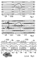
- FIG. 1 shows a second plurality made up of six second metallic conductors CO2 which exhibit various electrical connection points opposite positions CP. Said conductors could be word lines of a memory matrix. Beneath the second conductors CO2 and along their entire length there is a corresponding first plurality made up of six first conductors CO1 (not shown in FIG. 1), e.g. silicide, exhibiting various electrical connection points opposite the positions CP. Again opposite the positions CP there are provided VIAs permitting electrical connection between the conductors CO1 and the conductors CO2.
- FIG. 1 shows a defect D-0 such as to short circuit two adjacent conductors CO2.
- FIG. 2 shows the second conductors CO2 of FIG. 1 as modified in accordance with the present invention. As may be seen these are interrupted every two consecutive points CP and the breaks are in alternating positions. In the areas where the conductors CO2 are interrupted are visible the conductors CO1 which are however hidden by the conductors CO1 in the remaining areas. In this way there remain relatively large integrated circuit areas not traversed by conductors CO2. This means for example that the defect D-0 no longer causes any short circuit between the conductors CO2.
- the conductors CO1 depends on the specific application of the integrated circuit. In the case of memory devices they are parallel with each other while in another case they could for example be arranged as the spokes of a wheel.
- FIGS. 2 and 5 show two of the many possible choices.
- the positions CP are found in general at a constant distance every certain number of memory cells, e.g. 512. In other applications this might not be the optimal choice. In general the positions CP are determined on the basis of considerations on the electrical signal propagation time in the conductors CO1 and hence depend also on the type and number of electronic devices connected thereto.
- the conductors CO2 are advantageously of the same type as the conductors CO1 and are superimposed thereon.
- the electrical connection is then completed by means of VIAs. Naturally this is not indispensable for the purposes of the present invention.
- FIG. 3 shows a cross section view along plane of cut A-A of the conductors of FIG. 2 as if these belonged to a memory device.
- the first conductors CO1 which act as word lines of a memory device and are arranged above a substrate BU and separated therefrom by insulating layers IS.
- the substrate BU In the substrate BU are made pockets SO and DR which act as source and drain areas respectively for MOS devices constituting memory cells.
- a dielectric layer DL In which are arranged third metallic conductors CO3 acting as bit lines of the memory device.
- second conductors CO2 opposite some of the first conductors CO1.
- FIGS. 4 and 5 there is explained below an embodiment thereof suited specifically thereto.
- FIG. 4 shows a plurality of rows of such a memory device and three defects D-1, D-2 and D-3 caused by the process for making the rows in a metallic layer.
- the defect D-2 results in a short circuit between two adjacent rows and hence could be recovered by making use of redundancy.
- the defects D-1 and D-3 would cause rejection of the device since they involve a short circuit between four and six adjacent rows respectively.
- FIG. 4 was interrupted at several points giving rise to the rows of FIG. 5.
- pairs of rows were taken into consideration, the rows of each pair were interrupted at the same positions, and adjacent pairs were interrupted in alternating positions.
- the defect D-2 no long causes problems because it does not affect any row and the defects D-1 and D-3 affect a short circuit of only two adjacent rows and hence can be redundant without causing rejects.
Landscapes
- Semiconductor Memories (AREA)
- Internal Circuitry In Semiconductor Integrated Circuit Devices (AREA)
- Design And Manufacture Of Integrated Circuits (AREA)
Priority Applications (3)
| Application Number | Priority Date | Filing Date | Title |
|---|---|---|---|
| DE69422174T DE69422174T2 (de) | 1994-09-30 | 1994-09-30 | Integrierte Schaltung mit Toleranz bei wichtigen Herstellungsfehlern |
| EP94830468A EP0704901B1 (fr) | 1994-09-30 | 1994-09-30 | Circuit intégré tolérant des défauts majeurs de fabrication |
| US08/538,302 US5644526A (en) | 1994-09-30 | 1995-10-02 | Integrated circuit with improved immunity to large metallization defects |
Applications Claiming Priority (1)
| Application Number | Priority Date | Filing Date | Title |
|---|---|---|---|
| EP94830468A EP0704901B1 (fr) | 1994-09-30 | 1994-09-30 | Circuit intégré tolérant des défauts majeurs de fabrication |
Publications (2)
| Publication Number | Publication Date |
|---|---|
| EP0704901A1 true EP0704901A1 (fr) | 1996-04-03 |
| EP0704901B1 EP0704901B1 (fr) | 1999-12-15 |
Family
ID=8218545
Family Applications (1)
| Application Number | Title | Priority Date | Filing Date |
|---|---|---|---|
| EP94830468A Expired - Lifetime EP0704901B1 (fr) | 1994-09-30 | 1994-09-30 | Circuit intégré tolérant des défauts majeurs de fabrication |
Country Status (3)
| Country | Link |
|---|---|
| US (1) | US5644526A (fr) |
| EP (1) | EP0704901B1 (fr) |
| DE (1) | DE69422174T2 (fr) |
Families Citing this family (5)
| Publication number | Priority date | Publication date | Assignee | Title |
|---|---|---|---|---|
| US5933725A (en) * | 1998-05-27 | 1999-08-03 | Vanguard International Semiconductor Corporation | Word line resistance reduction method and design for high density memory with relaxed metal pitch |
| US5940315A (en) * | 1998-09-01 | 1999-08-17 | Micron Technology, Inc. | Strapped wordline architecture for semiconductor memory |
| US6549443B1 (en) * | 2001-05-16 | 2003-04-15 | Rockwell Collins, Inc. | Single event upset resistant semiconductor circuit element |
| US10685951B1 (en) * | 2018-12-10 | 2020-06-16 | Globalfoundries Inc. | Wordline strapping for non-volatile memory elements |
| US11004491B2 (en) | 2019-09-25 | 2021-05-11 | Globalfoundries U.S. Inc. | Twisted wordline structures |
Citations (1)
| Publication number | Priority date | Publication date | Assignee | Title |
|---|---|---|---|---|
| US4827449A (en) * | 1986-06-27 | 1989-05-02 | Oki Electric Industry Co., Ltd. | Semiconductor device |
Family Cites Families (3)
| Publication number | Priority date | Publication date | Assignee | Title |
|---|---|---|---|---|
| US4777387A (en) * | 1984-02-21 | 1988-10-11 | International Rectifier Corporation | Fast turn-off circuit for photovoltaic driven MOSFET |
| JPH0679263B2 (ja) * | 1987-05-15 | 1994-10-05 | 株式会社東芝 | 基準電位発生回路 |
| KR940008722B1 (ko) * | 1991-12-04 | 1994-09-26 | 삼성전자 주식회사 | 반도체 메모리 장치의 워드라인 드라이버 배열방법 |
-
1994
- 1994-09-30 EP EP94830468A patent/EP0704901B1/fr not_active Expired - Lifetime
- 1994-09-30 DE DE69422174T patent/DE69422174T2/de not_active Expired - Fee Related
-
1995
- 1995-10-02 US US08/538,302 patent/US5644526A/en not_active Expired - Lifetime
Patent Citations (1)
| Publication number | Priority date | Publication date | Assignee | Title |
|---|---|---|---|---|
| US4827449A (en) * | 1986-06-27 | 1989-05-02 | Oki Electric Industry Co., Ltd. | Semiconductor device |
Also Published As
| Publication number | Publication date |
|---|---|
| US5644526A (en) | 1997-07-01 |
| DE69422174D1 (de) | 2000-01-20 |
| DE69422174T2 (de) | 2000-08-24 |
| EP0704901B1 (fr) | 1999-12-15 |
Similar Documents
| Publication | Publication Date | Title |
|---|---|---|
| US6249472B1 (en) | Semiconductor memory device with antifuse | |
| EP2513909B1 (fr) | Réseau de mémoire programmable à antifusible | |
| US5684733A (en) | Fixed resistance high density parallel ROM device | |
| JP2863661B2 (ja) | 読出専用メモリ | |
| JPS63226943A (ja) | ゲートアレーデバイス用の基本セル | |
| US6686791B2 (en) | Oxide anti-fuse structure utilizing high voltage transistors | |
| US6067249A (en) | Layout of flash memory and formation method of the same | |
| US6856542B2 (en) | Programmable logic device circuit and method of fabricating same | |
| KR970008363B1 (ko) | 트리밍 회로 | |
| CN1322585C (zh) | 熔丝装置以及应用该装置的集成电路装置 | |
| CN114284272A (zh) | 小面积低电压反熔丝元件与阵列 | |
| US5867434A (en) | Integrated circuit memory devices having dummy memory cells therein for inhibiting memory failures | |
| US5841688A (en) | Matched delay word line strap | |
| JP2551340B2 (ja) | コンタクト抵抗測定用半導体集積回路装置およびその測定方法 | |
| US6188605B1 (en) | Non-volatile semiconductor memory using split bit lines | |
| EP0704901A1 (fr) | Circuit intégré tolérant des défauts majeurs de fabrication | |
| US5332917A (en) | Semiconductor memory NAND with wide space between selection lines | |
| CN107910316B (zh) | 半导体器件反熔丝结构及其写入和读取方法 | |
| KR0134854B1 (ko) | 반도체 장치의 설계장치 및 방법 | |
| EP0001164A1 (fr) | Mémoire morte intégrée | |
| KR100440410B1 (ko) | 다중레벨도전체워드라인스트래핑방식 | |
| US7683456B2 (en) | Semiconductor devices, capacitor antifuses, dynamic random access memories, and cell plate bias connection methods | |
| US20020011610A1 (en) | Semiconductor memory device having pairs of bit lines arranged on both sides of memory cells | |
| US9123428B2 (en) | E-fuse array circuit | |
| EP0817197B1 (fr) | Améliorations concernant des circuits intégrés |
Legal Events
| Date | Code | Title | Description |
|---|---|---|---|
| PUAI | Public reference made under article 153(3) epc to a published international application that has entered the european phase |
Free format text: ORIGINAL CODE: 0009012 |
|
| AK | Designated contracting states |
Kind code of ref document: A1 Designated state(s): DE FR GB IT |
|
| K1C1 | Correction of patent application (title page) published |
Effective date: 19960403 |
|
| 17P | Request for examination filed |
Effective date: 19960925 |
|
| 17Q | First examination report despatched |
Effective date: 19970429 |
|
| RAP3 | Party data changed (applicant data changed or rights of an application transferred) |
Owner name: STMICROELECTRONICS S.R.L. |
|
| GRAG | Despatch of communication of intention to grant |
Free format text: ORIGINAL CODE: EPIDOS AGRA |
|
| GRAG | Despatch of communication of intention to grant |
Free format text: ORIGINAL CODE: EPIDOS AGRA |
|
| GRAH | Despatch of communication of intention to grant a patent |
Free format text: ORIGINAL CODE: EPIDOS IGRA |
|
| GRAH | Despatch of communication of intention to grant a patent |
Free format text: ORIGINAL CODE: EPIDOS IGRA |
|
| GRAA | (expected) grant |
Free format text: ORIGINAL CODE: 0009210 |
|
| ITF | It: translation for a ep patent filed | ||
| AK | Designated contracting states |
Kind code of ref document: B1 Designated state(s): DE FR GB IT |
|
| ET | Fr: translation filed | ||
| REF | Corresponds to: |
Ref document number: 69422174 Country of ref document: DE Date of ref document: 20000120 |
|
| PLBE | No opposition filed within time limit |
Free format text: ORIGINAL CODE: 0009261 |
|
| STAA | Information on the status of an ep patent application or granted ep patent |
Free format text: STATUS: NO OPPOSITION FILED WITHIN TIME LIMIT |
|
| 26N | No opposition filed | ||
| REG | Reference to a national code |
Ref country code: GB Ref legal event code: IF02 |
|
| PGFP | Annual fee paid to national office [announced via postgrant information from national office to epo] |
Ref country code: DE Payment date: 20030909 Year of fee payment: 10 |
|
| PG25 | Lapsed in a contracting state [announced via postgrant information from national office to epo] |
Ref country code: DE Free format text: LAPSE BECAUSE OF NON-PAYMENT OF DUE FEES Effective date: 20050401 |
|
| PG25 | Lapsed in a contracting state [announced via postgrant information from national office to epo] |
Ref country code: IT Free format text: LAPSE BECAUSE OF NON-PAYMENT OF DUE FEES;WARNING: LAPSES OF ITALIAN PATENTS WITH EFFECTIVE DATE BEFORE 2007 MAY HAVE OCCURRED AT ANY TIME BEFORE 2007. THE CORRECT EFFECTIVE DATE MAY BE DIFFERENT FROM THE ONE RECORDED. Effective date: 20050930 |
|
| PGFP | Annual fee paid to national office [announced via postgrant information from national office to epo] |
Ref country code: GB Payment date: 20060217 Year of fee payment: 12 |
|
| PGFP | Annual fee paid to national office [announced via postgrant information from national office to epo] |
Ref country code: FR Payment date: 20060227 Year of fee payment: 12 |
|
| GBPC | Gb: european patent ceased through non-payment of renewal fee |
Effective date: 20060930 |
|
| REG | Reference to a national code |
Ref country code: FR Ref legal event code: ST Effective date: 20070531 |
|
| PG25 | Lapsed in a contracting state [announced via postgrant information from national office to epo] |
Ref country code: GB Free format text: LAPSE BECAUSE OF NON-PAYMENT OF DUE FEES Effective date: 20060930 |
|
| PG25 | Lapsed in a contracting state [announced via postgrant information from national office to epo] |
Ref country code: FR Free format text: LAPSE BECAUSE OF NON-PAYMENT OF DUE FEES Effective date: 20061002 |