EP0704902B1 - Application d'un dispositif semi-conducteur de puissance avec élément détecteur monolithiquement intégré - Google Patents
Application d'un dispositif semi-conducteur de puissance avec élément détecteur monolithiquement intégré Download PDFInfo
- Publication number
- EP0704902B1 EP0704902B1 EP95114638A EP95114638A EP0704902B1 EP 0704902 B1 EP0704902 B1 EP 0704902B1 EP 95114638 A EP95114638 A EP 95114638A EP 95114638 A EP95114638 A EP 95114638A EP 0704902 B1 EP0704902 B1 EP 0704902B1
- Authority
- EP
- European Patent Office
- Prior art keywords
- power semiconductor
- semiconductor device
- resistor
- current
- voltage
- Prior art date
- Legal status (The legal status is an assumption and is not a legal conclusion. Google has not performed a legal analysis and makes no representation as to the accuracy of the status listed.)
- Expired - Lifetime
Links
Images


Classifications
-
- H—ELECTRICITY
- H10—SEMICONDUCTOR DEVICES; ELECTRIC SOLID-STATE DEVICES NOT OTHERWISE PROVIDED FOR
- H10D—INORGANIC ELECTRIC SEMICONDUCTOR DEVICES
- H10D89/00—Aspects of integrated devices not covered by groups H10D84/00 - H10D88/00
- H10D89/10—Integrated device layouts
- H10D89/105—Integrated device layouts adapted for thermal considerations
Definitions
- the temperature, the load current and the saturation voltage (Forward voltage) of a power semiconductor component to Examples of an IGBT or MOS-FET are important operating parameters, their knowledge for a trouble-free and safe Operation of an electrical circuit with power semiconductor components
- the advantage is, overload conditions in good time recognized and, if necessary, suitable countermeasures for Protection of the component and connected consumers initiated can be.
- IGBTs with integrated sensors for load current detection are for example from the article by Bodo Arlt with the title “IGBT technology from the inventor” in the electronics industry magazine 1 - 1992, pages 14 to 18. Thereby with With the help of a current mirror a measuring current is generated, which with the help an external resistor into a resistor proportional to the load current Measuring voltage is implemented.
- a temperature increase for example with constant load current, however, this leads to an increase in the measuring voltage and feigns an increased load current.
- the result measurement error occurs especially when the Measuring resistance within the active area of the power semiconductor integrated and as a result together with the component of the load current is heated.
- WO 89/08928 is a Power semiconductor component with to the load transistor in Series of connected sensor cells, each with a resistor known, each with a load current and the Total voltage of the power semiconductor component representing voltage can be tapped. This is supposed to Determination of the power, the on-resistance and the Temperature of the power semiconductor device allows become. However, the determination of the load current points out the temperature dependence of the resistors not subject to temperature, by means of this sensor arrangement compensable error.
- the object on which the invention is based is now specify a power semiconductor device that an integrated Current sensor with integrated measuring resistor, where nevertheless a temperature-independent load current determination is possible.
- claims 2 to 6 relate to advantageous refinements of the invention Power semiconductor device, the characteristics of Claims 4 to 6 an additionally possible determination of Saturation voltage of the power semiconductor component affect.
- the features of claim 7 are based on a method temperature-independent determination of the load current of the Power semiconductor device directed during its operation.
- Figure 1 shows a simplified static equivalent circuit diagram of a power MOSFET according to the invention, with several, for Example three, sensor transistors ST1..ST3 and corresponding many measuring resistors.
- the sensor transistors and measuring resistors are monolithic together with the load transistor integrated and each switched as a current mirror, whereby the gate connections of the sensor transistors ST1..ST3 and Load transistor LT with a common external gate connection G, the drain connections sensor transistors ST1..ST3 and the load transistor LT with a common external Drain terminal D and respective source terminals 1..3 of the sensor transistors ST1..ST3 via respective measuring resistors R1..R3 and the source terminal of the load transistor LT directly to one common external source connection S are connected.
- the source connections 1..3 of the sensor transistors are available externally as component connections and lead, based on the reference potential of the source connection S, measuring voltages U1..U3, the voltage drops across the measuring resistors R1..R3 due to the load current I L being proportional Represent mirror currents I S1 ..I S3 .
- FIG. 2 shows an equivalent circuit diagram of a part of the component according to the invention, the part shown representing a current mirror from a respective sensor transistor, the load transistor and the measuring resistor Ri in the switched-on state.
- the equivalent circuit consists of a so-called bulk resistor R B , which is common to both the load transistor and the mirror transistor, an on-resistance r DM (on) of the sensor transistor, an on-resistance r A (on) of the load transistor and the measuring resistor Ri, whereby the resistor r DM (on) and the measuring resistor Ri are connected in series, the resistor r A (on) in parallel with this and this parallel connection of the resistor R B is in turn connected in series.
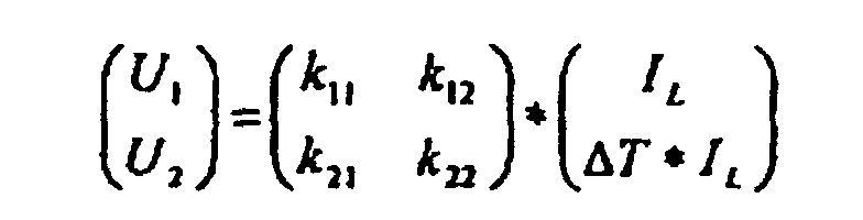
- the sensor arrangement can be described by the following system of equations.
- Figure 3 is an illustration of a part of an inventive Component, for example an IGBT with three Sensor transistors ST1..ST3 and three measuring resistors R1..R3, shown in top view.
- the measuring resistances are here all with a common main electrode, for example the emitter electrode E, connected on one side and on the other
- the measuring voltages are at the end of the respective measuring resistor U1..U3 on.
- the resistor R1 advantageously consists of polysilicon and the voltage U1 falling thereon is used to measure the load current I L.
- the resistor R2 is advantageously made of aluminum and the voltage U2 falling thereon is used to measure the temperature ⁇ T.
- the resistor R3 advantageously consists of polysilicon and the voltage U3 dropping thereon is used to measure the saturation voltage U CEsat .
- the accuracy of the sensor arrangement can be increased by suitable dimensioning of the current mirror, by a corresponding number of transistor cells, and by a suitable choice of the material of the measuring resistors.
- a current mirror with a large number of cells, for example with 12 cells, and a measuring resistor made of polysilicon with a low temperature coefficient of approximately 0.1% / K is suitable for measuring I L. Because of the high sheet resistance of polysilicon of approx. 9 ohms / square, it is also possible to produce a large measuring resistor of, for example,> 10 kOhm with relatively little space requirement, which together with a current mirror with a low number of cells, for example ⁇ 6 cells, as a sensor for U CEsat is well suited. Because of its higher temperature coefficient of approximately 0.4% / K, aluminum can advantageously be used as a resistance material for a sensor for temperature determination.
- FIG. 4 shows a sectional illustration of a power semiconductor component according to the invention, which has a semiconductor body H, on the structuring surface SO of which a non-conductive layer OX1, for example an SiO 2 layer, is provided, which has both a gate electrode GE and a resistance track for the measuring resistor R1 isolated from the semiconductor body H.
- This resistance path lies in a lateral area between two cells, a cell Z1 forming a cell of a sensor transistor and a cell Z2 of the load transistor LT and, like the gate electrode, made of polysilicon.
- a further non-conductive layer OX2, for example made of SiO 2 separates a metallic contacting layer consisting of two separate regions AL1 and Al2, which consists for example of aluminum, from the gate electrode GE.
- the area AL1 connects, through cutouts in the further oxide layer, cells Z1 of the sensor transistor with a first end and the area AL2, which represents the contacting layer for a main electrode, for example the electrode for an emitter connection E, with cells Z2 of the load transistor the other end of the resistance path for resistor R1.
- the gate electrode GE is connected to a gate connection G and a surface of the semiconductor body H facing away from the structuring surface SO is connected to a further main electrode, for example the electrode for a collector connection C.
- the high-resistance resistor R3 can be similar to the resistor R1 are made, the difference for example only in the course or in the length of the respective Resistance path.
- Resistors R1 and R3 are preferably shared with the gate electrode GE and the resistor R2 together with the Areas AL1 and AL2.
- Sensor arrangements with more than three sensor transistors and measuring resistors can also be used to measure the quantities I L , ⁇ T and U CEsat .
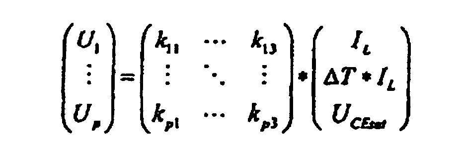
- the additional information increases the measuring accuracy by reducing the influence of statistical fluctuations in measured values (noise) and enables the consideration of non-linear components in the dependencies of the measuring voltages Ui on the influencing variables I L , U CEsat and in particular ⁇ T.
- K T * K is invertible, where K T is the transposed matrix K
Landscapes
- Semiconductor Integrated Circuits (AREA)
- Measurement Of Current Or Voltage (AREA)
- Insulated Gate Type Field-Effect Transistor (AREA)
Claims (9)
- Composant semi-conducteur de puissance,caractérisé en ce quedans lequel il est intégré monolithiquement, outre un transistor (LT) de charge, au moins deux autres transistors (ST1, ST2) et au moins deux résistances (R1, R2),dans lequel un premier circuit série constitué du premier autre transistor (ST1) et de la première résistance (R1) forme, ensemble avec le transistor (LT) de charge, un premier miroir de courant, etdans lequel un deuxième circuit série constitué du deuxième autre transistor (ST2) et de la deuxième résistance (R2) forme, ensemble avec le transistor (LT) de charge, un deuxième miroir de courant,une tension représentant le courant (IL) de charge du composant semi-conducteur de puissance pouvant être prélevée aux bornes de la première résistance (R1) pendant le fonctionnement du composant semi-conducteur de puissance,les pistes résistantes respectives des résistances sont en matériau ayant des coefficients de température différents, etla tension que l'on peut prélever aux bornes de la deuxième résistance (R2) pendant le fonctionnement du composant semi-conducteur de puissance sert à déterminer la température du composant semi-conducteur de puissance.
- Composant semi-conducteur de puissance suivant la revendication 1, caractérisé en ce que le matériau de la première résistance (R1) est essentiellement du polysilicium (POLY) et le matériau de la deuxième résistance (R2) est essentiellement de l'aluminium (AL).
- Composant semi-conducteur de puissance suivant la revendication 2, caractérisé en ce que le polysilicium est dopé pour régler son coefficient de température.
- Composant semi-conducteur de puissance suivant l'une des revendications précédentes, caractérisé en ce qu'en plus un troisième circuit série constitué d'un troisième autre transistor (ST3) et d'une troisième résistance (R3) forme, ensemble avec le transistor (LT) de charge, un troisième miroir de courant, la troisième résistance (R3) étant essentiellement en polysilicium et ayant une valeur ohmique plus grande d'au moins deux ordres de grandeur que la première et la deuxième résistance (R1, R2), de sorte que pendant le fonctionnement du composant semi-conducteur de puissance on peut prélever aux bornes de la troisième résistance (R3) une tension représentant la tension (UCEsat) de saturation du composant semi-conducteur de puissance.
- Composant semi-conducteur de puissance suivant la revendication 4, caractérisé en ce que le premier et le troisième autre transistor (ST1, ST3) sont constitués respectivement de cellules individuelles, le troisième autre transistor (ST3) ayant moins que la moitié du nombre de cellules du premier autre transistor (ST1).
- Composant semi-conducteur de puissance suivant la revendication 4 ou 5, caractérisé en ce que le premier circuit (ST1, R1) série et/ou le deuxième circuit (ST2, R2) série et/ou le troisième circuit (ST3, R3) série est prévu plusieurs fois.
- Procédé de détermination de la température et du courant de charge pendant le fonctionnement d'un composant semi-conducteur de puissance suivant l'une des revendications 1 à 6, comprenant les étapes :dans laquelle k1n et k2n avec n=1,2 sont des constantes de proportionnalité représentant des miroirs de courant du composant semi-conducteur de puissance.on prélève une première tension (U1) de mesure sur une première résistance (R1) eton prélève une deuxième tension (U2) de mesure sur une deuxième résistance (R2),on détermine le courant (IL) de charge et la température du composant semi-conducteur de puissance au moyen de la relation
- Procédé suivant la revendication 7, caractérisé en ce que l'on prélève en plus une troisième tension (U3) de mesure sur la troisième résistance et on détermine, outre la température et le courant de charge, la tension (UCEsat) de saturation du composant semi-conducteur de puissance au moyen de la relationdans laquelle k1n, k2n et k3n avec n=1,2,3 sont les constantes de proportionnalité représentant des miroirs de courant du composant semi-conducteur de puissance.

- Procédé suivant la revendication 8, caractérisé en ce que pour augmenter la précision de mesure, au moins l'un des trois miroirs (ST1, R1. ST2, R2, ST3, R3) de courant est prévu plusieurs fois et sert à la détermination d'une autre tension (Up) de mesure, de sorte que l'on dispose en tout de p miroirs de courant, la température, le courant (IL) de charge et la tension (UCEsat) de saturation étant déterminés au moyen de la relationdans laquelle k1n à kjn avec n=1,2,3 et j=1...p sont des constantes de proportionnalité représentant des miroirs de courant du composant semi-conducteur de puissance.
Applications Claiming Priority (2)
| Application Number | Priority Date | Filing Date | Title |
|---|---|---|---|
| DE4434894 | 1994-09-29 | ||
| DE4434894A DE4434894C2 (de) | 1994-09-29 | 1994-09-29 | Leistungshalbleiterbauelement mit monolithisch integrierter Sensoranordnung sowie seine Herstellung und Verwendung |
Publications (2)
| Publication Number | Publication Date |
|---|---|
| EP0704902A1 EP0704902A1 (fr) | 1996-04-03 |
| EP0704902B1 true EP0704902B1 (fr) | 2002-12-04 |
Family
ID=6529561
Family Applications (1)
| Application Number | Title | Priority Date | Filing Date |
|---|---|---|---|
| EP95114638A Expired - Lifetime EP0704902B1 (fr) | 1994-09-29 | 1995-09-18 | Application d'un dispositif semi-conducteur de puissance avec élément détecteur monolithiquement intégré |
Country Status (4)
| Country | Link |
|---|---|
| US (1) | US5663574A (fr) |
| EP (1) | EP0704902B1 (fr) |
| JP (1) | JPH08116058A (fr) |
| DE (2) | DE4434894C2 (fr) |
Families Citing this family (7)
| Publication number | Priority date | Publication date | Assignee | Title |
|---|---|---|---|---|
| DE19644193C2 (de) * | 1996-10-24 | 2001-04-19 | Bosch Gmbh Robert | Integrierte Überlastschutzeinrichtung mit Temperatursensor |
| JP3037191B2 (ja) * | 1997-04-22 | 2000-04-24 | 日本電気アイシーマイコンシステム株式会社 | 半導体装置 |
| US5942910A (en) * | 1997-08-28 | 1999-08-24 | Texas Instruments Incorporated | Method and circuit for providing accurate voltage sensing for a power transistor, or the like |
| DE10134665C1 (de) * | 2001-07-20 | 2002-09-05 | Infineon Technologies Ag | Betriebsverfahren für ein Halbleiterbauelement, geeignet für ESD-Schutz |
| DE10240914B4 (de) * | 2002-09-04 | 2007-01-25 | Infineon Technologies Ag | Schaltungsanordnung mit einem Lasttransistor und einer Strommessanordnung und Verfahren zur Ermittlung des Laststroms eines Lasttransistors sowie Verwendung eines Halbleiterbauelements |
| US7800171B2 (en) * | 2006-10-13 | 2010-09-21 | Infineon Technologies Austria Ag | Integrated circuit including a semiconductor device |
| US8057094B2 (en) * | 2007-11-16 | 2011-11-15 | Infineon Technologies Ag | Power semiconductor module with temperature measurement |
Family Cites Families (4)
| Publication number | Priority date | Publication date | Assignee | Title |
|---|---|---|---|---|
| US4472678A (en) * | 1981-08-10 | 1984-09-18 | Mostek Corporation | Test apparatus for circuits having a multiplex input/output terminal including a load connected to the terminal together with circuitry for monitoring the current flow through the load when inputting a signal to the terminal |
| US4931844A (en) * | 1988-03-09 | 1990-06-05 | Ixys Corporation | High power transistor with voltage, current, power, resistance, and temperature sensing capability |
| US5153696A (en) * | 1989-12-29 | 1992-10-06 | Nec Corporation | MOS FET with current sensing terminal |
| US5237262A (en) * | 1991-10-24 | 1993-08-17 | International Business Machines Corporation | Temperature compensated circuit for controlling load current |
-
1994
- 1994-09-29 DE DE4434894A patent/DE4434894C2/de not_active Expired - Fee Related
-
1995
- 1995-09-18 DE DE59510490T patent/DE59510490D1/de not_active Expired - Lifetime
- 1995-09-18 EP EP95114638A patent/EP0704902B1/fr not_active Expired - Lifetime
- 1995-09-29 JP JP7254020A patent/JPH08116058A/ja not_active Withdrawn
- 1995-09-29 US US08/536,607 patent/US5663574A/en not_active Expired - Lifetime
Also Published As
| Publication number | Publication date |
|---|---|
| DE59510490D1 (de) | 2003-01-16 |
| EP0704902A1 (fr) | 1996-04-03 |
| JPH08116058A (ja) | 1996-05-07 |
| DE4434894C2 (de) | 1998-07-02 |
| DE4434894A1 (de) | 1996-04-04 |
| US5663574A (en) | 1997-09-02 |
Similar Documents
| Publication | Publication Date | Title |
|---|---|---|
| DE60028282T2 (de) | Leistungshalbleitermodul | |
| EP1540748B1 (fr) | Capteur de champ magnetique pourvu d'un element a effet hall | |
| DE102009061841B3 (de) | Halbleiterchip | |
| DE102010028275B4 (de) | Integrierter Seebeck-Differenztemperatursensor und Verfahren zur Herstellung desselben | |
| DE68922795T2 (de) | Verfahren zum Messen des spezifischen Kontaktwiderstandes in integrierten Schaltungen. | |
| DE19823140B4 (de) | Abtast-Feldeffekttransistor | |
| DE69832954T2 (de) | Temperaturmessschaltung | |
| DE4192215B4 (de) | Halbleiterbauelement mit Temperaturerfassungsschaltung | |
| EP1279966B1 (fr) | Dispositif et procédé pour déterminer la fiabilité à hautes températures de circuits semi-conducteurs intégrés | |
| EP3608644B1 (fr) | Procédé de détermination d'un signe d'un courant de charge dans un circuit en pont avec au moins un commutateur de semi-conducteurs de puissance | |
| DE10031115A1 (de) | Halbleiterbauteil sowie Verfahren zur Messung seiner Temperatur | |
| EP0071269A2 (fr) | Détecteur d'empreintes digitales servant à la transformation d'une figure topologique d'un doigt à examiner, en un signal de sortie électrique | |
| DE102014112823B4 (de) | Halbleiterschalter mit integriertem Temperatursensor | |
| DE10240914B4 (de) | Schaltungsanordnung mit einem Lasttransistor und einer Strommessanordnung und Verfahren zur Ermittlung des Laststroms eines Lasttransistors sowie Verwendung eines Halbleiterbauelements | |
| DE102011076651B4 (de) | Stromregelung mit thermisch gepaarten Widerständen | |
| WO2012156126A2 (fr) | Élément de détection comportant un convertisseur piézoélectrique | |
| DE3425377C2 (de) | Pyroelektrischer Detektor | |
| DE102015108412A1 (de) | Integrierter Temperatursensor | |
| DE102016102478A1 (de) | Versatzspannungskompensation | |
| DE69325994T2 (de) | Integrierte Struktur eines Strom-Fühlwiderstandes für Leistungs-MOSFET-Vorrichtungen, insbesondere für Leistungs-MOSFET-Vorrichtungen mit einer Überstrom-Selbst-Schutzschaltung | |
| DE4434894C2 (de) | Leistungshalbleiterbauelement mit monolithisch integrierter Sensoranordnung sowie seine Herstellung und Verwendung | |
| EP0838856A2 (fr) | Dispositif intégré de protection contre des surcharges | |
| DE102014222214A1 (de) | Integrierte Halbleiterschaltung | |
| DE102014103513B4 (de) | Schaltungsanordnung und verfahren zum betreiben eines analog-digital-wandlers | |
| EP0704889A2 (fr) | Semi-conducteur de puissance avec résistance de mesure intégrée monolithique et fabrication |
Legal Events
| Date | Code | Title | Description |
|---|---|---|---|
| PUAI | Public reference made under article 153(3) epc to a published international application that has entered the european phase |
Free format text: ORIGINAL CODE: 0009012 |
|
| AK | Designated contracting states |
Kind code of ref document: A1 Designated state(s): CH DE GB IT LI |
|
| 17P | Request for examination filed |
Effective date: 19960419 |
|
| 17Q | First examination report despatched |
Effective date: 19971029 |
|
| RAP1 | Party data changed (applicant data changed or rights of an application transferred) |
Owner name: INFINEON TECHNOLOGIES AG |
|
| GRAG | Despatch of communication of intention to grant |
Free format text: ORIGINAL CODE: EPIDOS AGRA |
|
| RTI1 | Title (correction) |
Free format text: APPLICATION OF POWER SEMICONDUCTOR DEVICE WITH MONOLITHICALLY INTEGRATED SENSE DEVICE |
|
| RTI1 | Title (correction) |
Free format text: APPLICATION OF POWER SEMICONDUCTOR DEVICE WITH MONOLITHICALLY INTEGRATED SENSE DEVICE |
|
| GRAG | Despatch of communication of intention to grant |
Free format text: ORIGINAL CODE: EPIDOS AGRA |
|
| GRAH | Despatch of communication of intention to grant a patent |
Free format text: ORIGINAL CODE: EPIDOS IGRA |
|
| GRAH | Despatch of communication of intention to grant a patent |
Free format text: ORIGINAL CODE: EPIDOS IGRA |
|
| GRAA | (expected) grant |
Free format text: ORIGINAL CODE: 0009210 |
|
| AK | Designated contracting states |
Kind code of ref document: B1 Designated state(s): CH DE GB IT LI |
|
| REG | Reference to a national code |
Ref country code: GB Ref legal event code: FG4D Free format text: NOT ENGLISH |
|
| REG | Reference to a national code |
Ref country code: CH Ref legal event code: EP |
|
| REF | Corresponds to: |
Ref document number: 59510490 Country of ref document: DE Date of ref document: 20030116 |
|
| REG | Reference to a national code |
Ref country code: CH Ref legal event code: NV Representative=s name: INFINEON TECHNOLOGIES SCHWEIZ AG |
|
| GBT | Gb: translation of ep patent filed (gb section 77(6)(a)/1977) |
Effective date: 20030315 |
|
| PGFP | Annual fee paid to national office [announced via postgrant information from national office to epo] |
Ref country code: GB Payment date: 20030827 Year of fee payment: 9 |
|
| PGFP | Annual fee paid to national office [announced via postgrant information from national office to epo] |
Ref country code: CH Payment date: 20030901 Year of fee payment: 9 |
|
| PLBE | No opposition filed within time limit |
Free format text: ORIGINAL CODE: 0009261 |
|
| STAA | Information on the status of an ep patent application or granted ep patent |
Free format text: STATUS: NO OPPOSITION FILED WITHIN TIME LIMIT |
|
| 26N | No opposition filed |
Effective date: 20030905 |
|
| PG25 | Lapsed in a contracting state [announced via postgrant information from national office to epo] |
Ref country code: GB Free format text: LAPSE BECAUSE OF NON-PAYMENT OF DUE FEES Effective date: 20040918 |
|
| PG25 | Lapsed in a contracting state [announced via postgrant information from national office to epo] |
Ref country code: LI Free format text: LAPSE BECAUSE OF NON-PAYMENT OF DUE FEES Effective date: 20040930 Ref country code: CH Free format text: LAPSE BECAUSE OF NON-PAYMENT OF DUE FEES Effective date: 20040930 |
|
| GBPC | Gb: european patent ceased through non-payment of renewal fee |
Effective date: 20040918 |
|
| REG | Reference to a national code |
Ref country code: CH Ref legal event code: PL |
|
| PGFP | Annual fee paid to national office [announced via postgrant information from national office to epo] |
Ref country code: IT Payment date: 20070925 Year of fee payment: 13 |
|
| PG25 | Lapsed in a contracting state [announced via postgrant information from national office to epo] |
Ref country code: IT Free format text: LAPSE BECAUSE OF NON-PAYMENT OF DUE FEES Effective date: 20080918 |
|
| PGFP | Annual fee paid to national office [announced via postgrant information from national office to epo] |
Ref country code: DE Payment date: 20141121 Year of fee payment: 20 |
|
| REG | Reference to a national code |
Ref country code: DE Ref legal event code: R071 Ref document number: 59510490 Country of ref document: DE |