EP0704909B1 - Herstellungsverfahren für MOS-Halbleiterbauelement - Google Patents
Herstellungsverfahren für MOS-Halbleiterbauelement Download PDFInfo
- Publication number
- EP0704909B1 EP0704909B1 EP95306521A EP95306521A EP0704909B1 EP 0704909 B1 EP0704909 B1 EP 0704909B1 EP 95306521 A EP95306521 A EP 95306521A EP 95306521 A EP95306521 A EP 95306521A EP 0704909 B1 EP0704909 B1 EP 0704909B1
- Authority
- EP
- European Patent Office
- Prior art keywords
- layer
- forming
- strip
- midsection
- insulating support
- Prior art date
- Legal status (The legal status is an assumption and is not a legal conclusion. Google has not performed a legal analysis and makes no representation as to the accuracy of the status listed.)
- Expired - Lifetime
Links
Images

Classifications
-
- H—ELECTRICITY
- H10—SEMICONDUCTOR DEVICES; ELECTRIC SOLID-STATE DEVICES NOT OTHERWISE PROVIDED FOR
- H10D—INORGANIC ELECTRIC SEMICONDUCTOR DEVICES
- H10D30/00—Field-effect transistors [FET]
- H10D30/60—Insulated-gate field-effect transistors [IGFET]
- H10D30/67—Thin-film transistors [TFT]
- H10D30/6729—Thin-film transistors [TFT] characterised by the electrodes
- H10D30/673—Thin-film transistors [TFT] characterised by the electrodes characterised by the shapes, relative sizes or dispositions of the gate electrodes
- H10D30/6735—Thin-film transistors [TFT] characterised by the electrodes characterised by the shapes, relative sizes or dispositions of the gate electrodes having gates fully surrounding the channels, e.g. gate-all-around
-
- H—ELECTRICITY
- H10—SEMICONDUCTOR DEVICES; ELECTRIC SOLID-STATE DEVICES NOT OTHERWISE PROVIDED FOR
- H10D—INORGANIC ELECTRIC SEMICONDUCTOR DEVICES
- H10D30/00—Field-effect transistors [FET]
- H10D30/01—Manufacture or treatment
- H10D30/021—Manufacture or treatment of FETs having insulated gates [IGFET]
- H10D30/031—Manufacture or treatment of FETs having insulated gates [IGFET] of thin-film transistors [TFT]
- H10D30/0321—Manufacture or treatment of FETs having insulated gates [IGFET] of thin-film transistors [TFT] comprising silicon, e.g. amorphous silicon or polysilicon
- H10D30/0323—Manufacture or treatment of FETs having insulated gates [IGFET] of thin-film transistors [TFT] comprising silicon, e.g. amorphous silicon or polysilicon comprising monocrystalline silicon
-
- H—ELECTRICITY
- H10—SEMICONDUCTOR DEVICES; ELECTRIC SOLID-STATE DEVICES NOT OTHERWISE PROVIDED FOR
- H10D—INORGANIC ELECTRIC SEMICONDUCTOR DEVICES
- H10D30/00—Field-effect transistors [FET]
- H10D30/60—Insulated-gate field-effect transistors [IGFET]
- H10D30/67—Thin-film transistors [TFT]
- H10D30/6704—Thin-film transistors [TFT] having supplementary regions or layers in the thin films or in the insulated bulk substrates for controlling properties of the device
- H10D30/6713—Thin-film transistors [TFT] having supplementary regions or layers in the thin films or in the insulated bulk substrates for controlling properties of the device characterised by the properties of the source or drain regions, e.g. compositions or sectional shapes
- H10D30/6715—Thin-film transistors [TFT] having supplementary regions or layers in the thin films or in the insulated bulk substrates for controlling properties of the device characterised by the properties of the source or drain regions, e.g. compositions or sectional shapes characterised by the doping profiles, e.g. having lightly-doped source or drain extensions
-
- H—ELECTRICITY
- H10—SEMICONDUCTOR DEVICES; ELECTRIC SOLID-STATE DEVICES NOT OTHERWISE PROVIDED FOR
- H10D—INORGANIC ELECTRIC SEMICONDUCTOR DEVICES
- H10D30/00—Field-effect transistors [FET]
- H10D30/60—Insulated-gate field-effect transistors [IGFET]
- H10D30/67—Thin-film transistors [TFT]
- H10D30/6729—Thin-film transistors [TFT] characterised by the electrodes
- H10D30/673—Thin-film transistors [TFT] characterised by the electrodes characterised by the shapes, relative sizes or dispositions of the gate electrodes
-
- H—ELECTRICITY
- H10—SEMICONDUCTOR DEVICES; ELECTRIC SOLID-STATE DEVICES NOT OTHERWISE PROVIDED FOR
- H10D—INORGANIC ELECTRIC SEMICONDUCTOR DEVICES
- H10D30/00—Field-effect transistors [FET]
- H10D30/60—Insulated-gate field-effect transistors [IGFET]
- H10D30/67—Thin-film transistors [TFT]
- H10D30/6757—Thin-film transistors [TFT] characterised by the structure of the channel, e.g. transverse or longitudinal shape or doping profile
Definitions
- the present invention relates generally to semiconductor devices and more particularly to a thin-film transistor (TFT).
- TFT thin-film transistor
- TFTs prepared with hydrogenated amorphous silicon were studied for thin-film image sensor applications. Recrystallization of this or similar material led to relatively high performance poly TFTs.
- poly TFTs were applied in production quantities to active-matrix-type liquid crystal displays (LCDs). These products use glass or quartz substrates.
- the TFTs are relatively large in size compared to conventional MOS transistors and operate at higher voltages than those commonly used in digital applications.
- Hayden et al. "A High-Performance Quadruple Well, Quadruple Poly BiCMOS Process for Fast 16 Mb SRAMs," IEEE IEDM , pg. 819 (1992) reported in 1992 an experimental SRAM cell, see Koichiro Ishibashi et al., "A IV TFT-Load SRAM Using a Two-Step Word-Voltage Method, IEEE ISSCC , pg. 206 (1992).
- a TFT may be used as a load device in a static random access memory (SRAM) cell.
- SRAM static random access memory
- a TFT is a field-effect transistor (FET) having its channel, drain, and source regions formed from a strip of semiconductor material that has been formed on a dielectric substrate, such as quartz or glass.
- FET field-effect transistor
- a TFT may be formed in vertical alignment with a semiconductor structure, such as an SRAM cell.
- Such stacking of integrated-circuit components often provides a significant reduction in the area of the integrated circuit.
- TFTs often exhibit significantly lower "on" currents, I dsat , than do their conventional counterparts with similar W/L ratios. Additionally, the switching speed of a TFT is often too slow for certain applications.
- J.P. Colinge et al., "Silicon-On-Insulator Gate-All-Around Device," IEDM, 1990, EP-A-0418983, US-5120666 and EP-A-0612103 disclose methods of manufacturing TFTs having gate electrodes encircling the channel. However, each of those documents discloses forming the upper portion of the gate electrode by conventional patterning and etching process steps.
- the inventive process involves forming a cavity below a poly film patterned into narrow strips.
- the poly layer is used to form the channel, and source and drain regions of the TFT.
- the cavity and a channel or slot are provided into the dielectric substrate using standard photoresist methods and etching techniques.
- a second film of highly conformal LPCVD poly is then let into the cavity and channel somewhat analogous to the "damascene" process, used for metal layers and reported in recent years by IBM. See, R.R. Uttecht and Robert M. Geffken, "A Four-Level-Metal Fully Planarized Interconnect Technology For Dense High Performance Logic and SRAM Applications," VMIC , pg. 20 (1991).
- the second poly film forms a self-aligned gate electrode around the transistor channel region in the thin first poly film.
- Functional n- or p-channel transistors are created using only two photomasking steps.
- the minimum transistor length is 4 ⁇ , where ⁇ is the minimum feature size. This compares to standard MOS technology, which provides minimum poly line widths (transistor lengths as viewed from the surface of the wafer) of 2 ⁇ .
- a semiconductor device which includes an insulating support, is provided.
- a strip of semiconductor material has a pair of opposing ends in contact with the insulating support and a midsection extending between the ends.
- a layer of dielectric material encircles the midsection, and a layer of conductive material encircles the dielectric layer.
- the illustrated semiconductor device may be a TFT formed on a dielectric substrate.
- the opposing ends form the source and drain regions respectively, and the midsection forms the channel region.
- the dielectric layer and the conductive layer form the gate insulator and the gate electrode respectively.
- the source and drain regions respectively include lightly doped source and drain regions.
- An advantage provided by one aspect of the present invention is an increase in "on" current without an increase in either V ds or V gs .
- An advantage provided by another aspect of the present invention is an increase in switching speed.
- a semiconductor device comprising an insulating support having a cavity disposed therein; a strip of semiconductor material having two ends contacting said insulating support and a midsection extending between said ends over said cavity; a layer of dielectric material encircling said midsection; and a layer of conductive material encircling said dielectric layer and having an upper portion and lower portion, characterised in that; said upper and lower portions of said layer of conductive material are self-aligned to said midsection.
- Said insulating support may comprise a dielectric material.
- Said semiconductor material may comprise polysilicon.
- a first of said ends may form a drain region, a second of said ends may form a source region, and said midsection may form a channel region.
- Said condcutive layer may form a gate electrode.
- Said midsection may be substantially planar with respect of said ends and said insulating support.
- Said dielectric layer may form a gate insulator.
- Said source region and said drain region may each comprise a lightly doped region adjacent to said channel region.
- Said gate insulator may comprise silicon dioxide.
- Said gate electrode may comprise polysilicon.
- Said semiconductor material may comprise polysilicon.
- a method for forming a semiconductor device comprising forming a strip of semiconductor material on an insulating support, forming a layer of material on said strip of semiconductor material and on said insulating support; forming a cavity in said layer of material and in said insulating support around a midsection of said strip; forming an insulator around said midsection; and filling said cavity with a conductive material to form a gate electrode around said insulator whereby said electrode has an upper and a lower portion which are self-aligned to said midsection of said strip, wherein said upper portion is defined by said cavity in said layer of mateial and said lower portion is defined by said cavity in said insulating support.
- the method may further comprise doping said midsection to form a channel region and doping ends of said strip adjacent said midsection to form source and drain regions.
- the method may further comprise lightly doping portions of said source and drain regions adjacent said channel region to form lightly doped source and drain regions.
- Said step of forming a strip may comprise forming a layer of polysilicon on said insulating support, and etching said layer of polysilicon to form said strip.
- Said step of forming a strip may comprise forming a layer of amorphous silicon on said insulating support, etching said layer of amorphous silicon to form said strip, forming a first dielectric layer over said insulating support and said strip, forming a second dielectric layer over said first dielectric layer, and flowing said first and second dielectric layers to form a planar surface and to convert said amorphous silicon into polysilicon.
- said step of forming said cavity comprises forming on said layer of material a mask that exposes said midsection, anisotropically etching said layer and said insulating support to form openings adjacent sides of said midsection, and isotropically etching said insulating support such that said openings merge beneath said midsection to form said cavity.
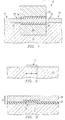
- Figure 1 is a cross-sectional view of a semiconductor device 10 shown as an illustrative example to and understanding according to the present invention.
- Device 10 which is an FET, includes an insulating support 12 and a strip of semiconductor material 14.
- the insulating support 12 may be formed from a dielectric such as SiO 2 or glass over a semiconductor substrate, and strip 14 is formed from polysilicon to form a TFT.
- Strip 14 includes a channel 16 and source and drain regions 18 and 20.
- a gate insulator 22 encircles channel 16, and a gate electrode 24 encircles gate insulator 22.
- gate electrode 24 completely encircles channel 16, the on current and transconductance of device 10 is increased approximately 2-5 times greater than the on current and transconductance of a device having a gate electrode along only a top portion of the channel 16 surface. Additionally, device 10 may include lightly doped source and drain regions 26 and 28, which lower the electric field at drain 20 to reduce the tendency of electrons from drain 20 to become lodged in gate insulator 22. Such lodging, commonly referred to as the "hot electron” problem, may over time shift the threshold voltage of device 10. Furthermore, as discussed below, gate electrode 24 is self-aligned to channel 16. Such self-alignment significantly reduces the size of the device and also reduces parasitic capacitances such as the Miller capacitance, and therefore increases the switching speed of device 10.
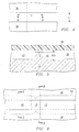
- Figures 2 - 10 illustrate a method according to an embodiment of the present invention for forming device 10.
- strip 14 of semiconductor material having width W, is formed on an insulating support 12.
- the strip 14 is a layer of amorphous silicon deposited on insulating support 12, which is an SiO 2 layer over a silicon substrate, with a low pressure chemical vapor deposition (LPCVD) process.
- the thickness of the amorphous silicon film is in the range of approximately 500 - 2500 ⁇ . Typically, the thinner the film, the lower the threshold voltage of the TFT.
- the deposition temperature is preferably kept between 475 - 650°C so that few nuclei are present for the subsequent grain growth process.
- the amorphous silicon may be deposited using a source gas of either SiH 4 , which is the conventional gas used, or Si 2 H 6 .
- Si 2 H 6 allows the LPCVD to be performed at approximately 475°C and still produce a film that is acceptable.
- the insulating support 12 may be glass or quartz.
- An LPCVD process at such a low temperature (approximately 475°C) allows insulating support 12 to be glass or quartz.
- the silicon film 14 may be formed as polysilicon. Typical polysilicon formation temperatures range from 650 - 950°C for forming polysilicon on an SiO 2 layer over a silicon substrate. In one embodiment, this polysilicon film may then be made amorphous by ion implantation of silicon. Typically, an implantation level of about 5 x 10 15 atoms/cm 2 at about 75 KEV is sufficient, although the level may vary depending upon the thickness of the deposited film. The growth conditions, and subsequent implant, if necessary, should be such that the deposited film is made as amorphous as possible. Alternatively, the strip 14 may remain polycrystalline silicon and the inventive device formed from polycrystalline silicon as the channel, source and drain regions 16, 18, and 20.
- the amorphous silicon film 14 is exposed to a relatively long, low temperature anneal in N 2 or AR to convert the amorphous silicon to large grained polysilicon.
- this anneal is performed at temperatures approximately in the range of 475 - 600°C and for a time period approximately in the range of 20 - 100 hours.
- the temperature during the annealing process is low enough to prohibit the generation of additional nucleation sites or small crystals, but high enough to allow existing crystallites to grow through solid-state diffusion.
- Such an annealing process produces a polysilicon film having grain sizes of approximately 5 ⁇ m and larger.
- the amorphous silicon film may be converted to large gram polysilicon by using existing laser recrystallization methods.
- the amorphous silicon film is converted into large-grained polysilicon because larger grains produce improved TFTs.
- the larger grains typically reduce the number of charges that may be stored at carrier traps located mainly at the grain boundaries.
- small grains often generate many such traps, which often force a significant portion of the gate voltage applied to the TFT to be wasted in the work of charging and discharging these trap sites instead of creating an inversion layer, i.e., forming the channel, to turn the TFT on.
- the polysilicon layer may be passivated with hydrogen (H). Such passivation reduces the threshold voltage and sub threshold leakage currents of the TFT.
- the polysilicon layer may be hydrogen passivated, including a long bake in an appropriate forming gas or H, applying plasma-enhanced chemical vapor deposition (PECVD) silicon nitride layers, immersing the semiconductor structure 10 in a hydrogen plasma at approximately 300°C, or by high-dose ion implantation with protons.
- PECVD plasma-enhanced chemical vapor deposition
- acceptably large grained polycrystalline silicon may be formed for strip 14 using any suitable technique, including the direct formation of polysilicon on a glass or SiO 2 layer.
- width W is 2 ⁇ , where 2 ⁇ is the minimum feature-size capability for the width of the polysilicon layer 14 for the process technology being used.
- a planar layer 30 is formed over insulating support 12 and strip 14.
- layer 30 includes a layer 32 of silicon dioxide (SiO 2 ) that is approximately 2,000 ⁇ thick, and a layer 34 of phosphorous glass or boron doped glass that is approximately 5,000 ⁇ thick.
- Layer 34 is then flowed to give a planar surface 36.
- SiO 2 layer 32 is deposited using either a conformal chemical vapor deposition or a low pressure chemical vapor deposition.
- layer 34 is flowed at an appropriate temperature, typically in the range of 800°-1100°C for some applications, though lower temperatures may be used if desired to give approximately flat upper surface 36.
- layer 30 having planar surface 36 may be formed from a spin-on glass film using existing techniques. This is useful for LCDs formed on glass or quartz.
- a photoresist mask 38 is formed on the surface and etched to expose midsection 16, which has a length L. In one embodiment of the invention, length L is approximately equal to width W.
- the exposed portions of layer 30 and insulating support 12 are anisotropically etched to give a structure having the view shown in Figure 5 taken along lines A-A of Figure 4.
- An anisotropic etch process having a high SiO 2 to Si selectivity is preferred. Such an anisotropic etch may be performed using existing ion-assisted plasma etch processes that use various fluorocarbon plasma chemistries.
- the anisotropic etch completely removes'the exposed portion of layer 30 and etches into insulating support 12 a depth of approximately ⁇ , which is about W/2, below the bottom of the midsection 16.
- this anisotropic etch forms on either side of strip 14, at the midsection 16, open regions 42.
- the exposed portions of insulating support 12 and layer 30 are then isotropically etched to give an undercut whose boundary is shown by dotted line 40.
- the amount of undercut within regions 42 is such that an intermediate cavity 46 (Figure 7), which is beneath midsection 16, is formed because the insulating layer 12 is etched through under the midsection 16.
- Such an isotropic etch may be performed using an aqueous solution of HF, such as buffered oxide etch (BOE), to a desired depth. In one embodiment, a depth approximately W/2 beyond the original depth of openings 42 after the anisotropic etch is appropriate. However, a smaller undercut is desired in some designs and, for a large gate electrode, a larger undercut is desired, as much as 2 ⁇ or greater.
- FIG 7 is a cross-sectional view taken along lines B-B of Figure 6, one can see that cavity 46 is formed beneath midsection 16 of strip 14.
- the dotted line shows the depth of openings 42 and the solid line the cavity 46 after the isotropic etch.
- a gate insulator or dielectric 48 is formed such that it completely encircles midsection 16 of strip 14. Because the length of midsection 16 is defined by the width of cavity 46, the gate electrode will be self-aligned with midsection 16, which will become the channel region of the TFT. Such self-alignment will reduce the Miller parasitic capacitance, which can be increased if the gate electrode overlaps the source or drain regions 18 and 20 ( Figure 1).
- the thickness of gate insulator 48 may vary within the range of approximately 150 - 500 ⁇ , depending upon the desired threshold voltage.
- Gate insulator 48 may be formed using a combination of thermal oxidation followed by conformal CVD of tetra-ethyl-ortho-silicate (TEOS)-based silicon dioxide.
- gate insulator 48 may be grown thermally in dry oxygen (O 2 ).
- gate insulator 48 may be formed using only CVD as is used to form existing TFTs, or using a chemical-vapor deposited silicon-nitride-gate dielectric process.
- the exposed midsection 16 can be thinned by light oxidation and a BOE etching if desired to form a specific-size device.
- midsection 16 is implanted with a suitable dopant to form the channel of the TFT.
- a suitable dopant for example, to form an N-channel transistor, midsection 16 may be implanted with boron in the range of approximately 10 12 atoms/cm 2 .
- channel region 16 may be left undoped, though typically the channel 16 is lightly implanted with arsenic (As), to have the desired threshold characteristics selected by the designer using known design tools.
- Mask layer 38 is removed either before or after midsection 16 is implanted to form the channel 16.
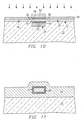
- structure 10 is then coated with a layer 50 of polysilicon. As shown, layer 50 completely fills in openings 42 and cavity 46 to completely encircle both gate oxide 48 and channel 16. Depending upon the deposition process used, some voids 52 may exist in the portion of polysilicon layer 50 in the cavity 46 beneath channel 16. However, it is believed that such voids have no adverse effect on the performance of the resulting TFT, and may be avoided altogether in some polysilicon deposition techniques.
- polysilicon layer 50 is doped and etched to the surface of glass layer 30.
- polysilicon layer 50 is first doped with an N + implant or diffusion.
- the top portion of layer 50 may be removed with existing processes, such as chemical mechanical polishing (CMP), or if photoresist mask 38 has small enough openings, an anisotropic plasma etch may be used to remove the poly layer 50.
- CMP chemical mechanical polishing
- an anisotropic plasma etch may be used to remove the poly layer 50.
- the plasma chemistry should have a high selectivity of Si to SiO 2 such as that found in SF 6 -based ion-assisted plasma etching.
- the top portion of layer 50 may be etched first, and the portion of layer 50 remaining in cavity 46 and openings 42, i.e., the portion of layer 50 that forms gate electrode 24, may be doped afterwards.
- the upper portion 54 of gate electrode 24 may be more highly doped than the lower portion.
- layer 30 may be removed, and the end portions of strip 14 adjacent to channel 16 may be suitably doped to form source and drain regions 18 and 20 (Figure 1) of the TFT.
- the doping of the source and drain regions 18 and 20 also implants dopant into the top and exposed sidewall portions of the gate electrode 24.
- a later diffusing step will drive the dopant under the channel 16, into lower portions 54 to ensure that it is doped, if it has not already been doped in a previous step.
- the source and drain regions 18 and 20 are thus also formed as self-aligned with the gate electrode 24.
- the layer 30 is etched back using an appropriate masking scheme to form spacers 56.
- the width S of spacers 56 is approximately 0.5 ⁇ m.
- the on/off current ratio for the resulting TFT is approximately 10 4 as compared to 10 2 for non-LDD devices.
- the on/off current ratio where S equals approximately 0.45 ⁇ m is approximately 10 7 .
- strip 14 is implanted with a dopant.
- layer 14 is doped with As using an implant level of approximately 10 15 atom/cm 2 to form N+ source and drain regions 18 and 20, which in Figure 9 would begin at the outer edges of spacers 56.
- spacers 56 may then be removed such as with a BOE or plasma etching.
- a light dose of dopant is implanted to form lightly-doped regions 26 and 28 of an LDD-type structure.
- the LDD structure is thus self-aligned with the gate electrode and channel region using side wall oxide spacers, providing significant size and device operation features not previously possible in polysilicon devices formed over an insulating substrate.
- a light dose of a value appropriate for LDD devices of As is implanted through an applied oxide layer 58.
- the structure 10 may then be lightly oxidized to heal any edge voids in the gate dielectric 48.
- the dopants may then be activated by using rapid thermal annealing (RTA) to reduce lateral diffusion.
- RTA rapid thermal annealing
- a light dopant implant may be performed to form drain regions 18 and 20 from a lightly doped material.
- spacers 56 are formed and a second implant is performed such that regions 26 and 28 beneath spacer 16 remain lightly doped and the remaining portions of source and drain 18 and 20 become highly doped to give a resulting TFT with lightly doped drain and source regions 26 and 28.
- Figure 11 shows a cross-sectional view of the completed TFT as viewed along lines AA of Figure 4.
- the appropriate electrical interconnections to the source and drain regions 18 and 20 are made using vias, contacts, or the like so that the polysilicon transistor 10 can become an element of a larger circuit.
- the contacts can be from a lower layer to a device 10 or from a higher layer.
- the electrical interconnections will contact source/drain regions 18 and 20 to respective conductors in the circuit, and the gate electrode 24 to another conductor to provide transistor operations, diode connections, load connections, or the like, as required for each circuit design.
- the standard techniques known in the art today for forming electrical contacts to poly one, poly two, and other layers, may be used.
Landscapes
- Thin Film Transistor (AREA)
Claims (5)
- Verfahren zum Bilden einer Halbleitereinrichtung, mit den folgenden Schritten:ein Streifen aus einem Halbleitermaterial (14) wird auf einem isolierenden Träger (12) gebildet,eine Schicht aus Material (30) wird auf dem Streifen aus Halbleitermaterial (14) und auf dem isolierenden Träger (12) gebildet;eine Vertiefung (46) wird in der Schicht aus Material (30) und in dem isolierenden Träger (12) um einen Mittelabschnitt (16) des Streifens herum gebildet;ein Isolator (48) wird um den Mittelabschnitt (16) gebildet; unddie Vertiefung wird mit einem leitenden Material gefüllt, um eine Gateelektrode (24) um den Isolator (22) herum zu bilden, so dass die Elektrode (24) einen oberen und einen unteren Abschnitt aufweist, die mit dem Mittelabschnitt (16) des Streifens selbstausgerichtet sind, wobei der obere Abschnitt durch die Vertiefung in der Schicht aus Material definiert ist und der untere Abschnitt durch die Vertiefung in dem isolierenden Träger definiert ist.
- Verfahren nach Anspruch 1, bei dem der Schritt zum Bilden der Vertiefung umfasst:auf der Schicht aus Material (30) wird eine Maske (38) gebildet, die den Mittelabschnitt (16) exponiert;die Schicht (30) und der isolierende Träger (16) werden anisotrop geätzt, um Öffnungen (42) zu bilden, die an die Seiten des Mittelabschnitts (16) angrenzen; undder isolierende Träger (12) wird isotrop geätzt, so dass die Öffnungen (42) unterhalb des Mittelabschnitts (16) zusammenlaufen, um die Vertiefung (46) zu bilden.
- Verfahren nach einem vorhergehenden Anspruch, mit dem weiteren Schritt, dass der Mittelabschnitt (16) dotiert wird, um einen Kanalbereich zu bilden, und dass Enden des Streifens angrenzend an den Mittelabschnitt dotiert werden, um Source- (18) und Drainbereiche (20) zu bilden.
- Verfahren nach einem vorhergehenden Anspruch, bei dem der Schritt zum Bilden eines Streifens (14) umfasst:eine Schicht aus Polysilizium wird auf dem isolierenden Träger (12) gebildet; unddie Schicht aus Polysilizium wird geätzt, um den Streifen (14) zu bilden.
- Verfahren nach einem der Ansprüche 1 bis 3, bei dem der Schritt zum Bilden eines Streifens umfasst:eine Schicht aus amorphem Silizium wird auf dem isolierenden Träger (12) gebildet;die Schicht aus amorphem Silizium wird geätzt, um den Streifen (14) zu bilden;eine erste dielektrische Schicht (32) wird über dem isolierenden Träger (12) und dem Streifen (14) gebildet;eine zweite dielektrische Schicht (34) wird über der ersten dielektrischen Schicht (32) gebildet; undman lässt die erste (32) und zweite (34) dielektrische Schicht fließen, um eine planare Oberfläche (30) zu bilden und das amorphe Silizium in Polysilizium umzuwandeln.
Applications Claiming Priority (2)
| Application Number | Priority Date | Filing Date | Title |
|---|---|---|---|
| US315955 | 1994-09-30 | ||
| US08/315,955 US5705405A (en) | 1994-09-30 | 1994-09-30 | Method of making the film transistor with all-around gate electrode |
Publications (3)
| Publication Number | Publication Date |
|---|---|
| EP0704909A2 EP0704909A2 (de) | 1996-04-03 |
| EP0704909A3 EP0704909A3 (de) | 1997-09-10 |
| EP0704909B1 true EP0704909B1 (de) | 2001-07-04 |
Family
ID=23226822
Family Applications (1)
| Application Number | Title | Priority Date | Filing Date |
|---|---|---|---|
| EP95306521A Expired - Lifetime EP0704909B1 (de) | 1994-09-30 | 1995-09-15 | Herstellungsverfahren für MOS-Halbleiterbauelement |
Country Status (4)
| Country | Link |
|---|---|
| US (2) | US5705405A (de) |
| EP (1) | EP0704909B1 (de) |
| JP (1) | JP3869037B2 (de) |
| DE (1) | DE69521579T2 (de) |
Families Citing this family (48)
| Publication number | Priority date | Publication date | Assignee | Title |
|---|---|---|---|---|
| US6060375A (en) * | 1996-07-31 | 2000-05-09 | Lsi Logic Corporation | Process for forming re-entrant geometry for gate electrode of integrated circuit structure |
| US6962883B2 (en) * | 1996-08-01 | 2005-11-08 | Texas Instruments Incorporated | Integrated circuit insulator and method |
| KR100331845B1 (ko) * | 1998-01-10 | 2002-05-10 | 박종섭 | 박막트랜지스터제조방법 |
| US6117712A (en) * | 1998-03-13 | 2000-09-12 | Texas Instruments - Acer Incorporated | Method of forming ultra-short channel and elevated S/D MOSFETS with a metal gate on SOI substrate |
| US6207530B1 (en) | 1998-06-19 | 2001-03-27 | International Business Machines Corporation | Dual gate FET and process |
| DE69832162D1 (de) * | 1998-07-22 | 2005-12-08 | St Microelectronics Srl | Herstellungsverfahren für ein elektronisches Bauelement, das MOS Transistoren mit salizidierten Übergängen und nicht salizidierten Widerständen enthält |
| US6162688A (en) * | 1999-01-14 | 2000-12-19 | Advanced Micro Devices, Inc. | Method of fabricating a transistor with a dielectric underlayer and device incorporating same |
| US6103563A (en) * | 1999-03-17 | 2000-08-15 | Advanced Micro Devices, Inc. | Nitride disposable spacer to reduce mask count in CMOS transistor formation |
| DE19924571C2 (de) | 1999-05-28 | 2001-03-15 | Siemens Ag | Verfahren zur Herstellung eines Doppel-Gate-MOSFET-Transistors |
| DE19928564A1 (de) * | 1999-06-22 | 2001-01-04 | Infineon Technologies Ag | Mehrkanal-MOSFET und Verfahren zu seiner Herstellung |
| FR2799305B1 (fr) * | 1999-10-05 | 2004-06-18 | St Microelectronics Sa | Procede de fabrication d'un dispositif semi-conducteur a grille enveloppante et dispositif obtenu |
| US6376286B1 (en) * | 1999-10-20 | 2002-04-23 | Advanced Micro Devices, Inc. | Field effect transistor with non-floating body and method for forming same on a bulk silicon wafer |
| US6465852B1 (en) | 1999-10-20 | 2002-10-15 | Advanced Micro Devices, Inc. | Silicon wafer including both bulk and SOI regions and method for forming same on a bulk silicon wafer |
| US6245636B1 (en) | 1999-10-20 | 2001-06-12 | Advanced Micro Devices, Inc. | Method of formation of pseudo-SOI structures with direct contact of transistor body to the substrate |
| US6391658B1 (en) * | 1999-10-26 | 2002-05-21 | International Business Machines Corporation | Formation of arrays of microelectronic elements |
| WO2001065609A1 (en) * | 2000-02-29 | 2001-09-07 | Koninklijke Philips Electronics N.V. | Semiconductor device and method of manufacturing same |
| DE10012112C2 (de) * | 2000-03-13 | 2002-01-10 | Infineon Technologies Ag | Steg-Feldeffekttransistor und Verfahren zum Herstellen eines Steg-Feldeffekttransistors |
| US6982460B1 (en) * | 2000-07-07 | 2006-01-03 | International Business Machines Corporation | Self-aligned gate MOSFET with separate gates |
| US6563131B1 (en) | 2000-06-02 | 2003-05-13 | International Business Machines Corporation | Method and structure of a dual/wrap-around gate field effect transistor |
| JP2002034179A (ja) * | 2000-07-14 | 2002-01-31 | Toshiba Corp | 電力制御装置 |
| DE10045045C2 (de) * | 2000-09-12 | 2002-09-19 | Infineon Technologies Ag | Herstellungsverfahren von Feldeffekttransistoren in integrierten Halbleiterschaltungen |
| FR2822293B1 (fr) * | 2001-03-13 | 2007-03-23 | Nat Inst Of Advanced Ind Scien | Transistor a effet de champ et double grille, circuit integre comportant ce transistor, et procede de fabrication de ce dernier |
| US6982194B2 (en) * | 2001-03-27 | 2006-01-03 | Semiconductor Energy Laboratory Co., Ltd. | Semiconductor device and method for manufacturing the same |
| US7189997B2 (en) | 2001-03-27 | 2007-03-13 | Semiconductor Energy Laboratory Co., Ltd. | Semiconductor device and method for manufacturing the same |
| US6740938B2 (en) * | 2001-04-16 | 2004-05-25 | Semiconductor Energy Laboratory Co., Ltd. | Transistor provided with first and second gate electrodes with channel region therebetween |
| FR2838238B1 (fr) * | 2002-04-08 | 2005-04-15 | St Microelectronics Sa | Dispositif semiconducteur a grille enveloppante encapsule dans un milieu isolant |
| US7074623B2 (en) * | 2002-06-07 | 2006-07-11 | Amberwave Systems Corporation | Methods of forming strained-semiconductor-on-insulator finFET device structures |
| US20030227057A1 (en) * | 2002-06-07 | 2003-12-11 | Lochtefeld Anthony J. | Strained-semiconductor-on-insulator device structures |
| US6995430B2 (en) * | 2002-06-07 | 2006-02-07 | Amberwave Systems Corporation | Strained-semiconductor-on-insulator device structures |
| US6833588B2 (en) * | 2002-10-22 | 2004-12-21 | Advanced Micro Devices, Inc. | Semiconductor device having a U-shaped gate structure |
| US6686231B1 (en) * | 2002-12-06 | 2004-02-03 | Advanced Micro Devices, Inc. | Damascene gate process with sacrificial oxide in semiconductor devices |
| US6864164B1 (en) | 2002-12-17 | 2005-03-08 | Advanced Micro Devices, Inc. | Finfet gate formation using reverse trim of dummy gate |
| US6855606B2 (en) * | 2003-02-20 | 2005-02-15 | Taiwan Semiconductor Manufacturing Company, Ltd. | Semiconductor nano-rod devices |
| US7074656B2 (en) * | 2003-04-29 | 2006-07-11 | Taiwan Semiconductor Manufacturing Company, Ltd. | Doping of semiconductor fin devices |
| KR100471173B1 (ko) | 2003-05-15 | 2005-03-10 | 삼성전자주식회사 | 다층채널을 갖는 트랜지스터 및 그 제조방법 |
| US6855582B1 (en) | 2003-06-12 | 2005-02-15 | Advanced Micro Devices, Inc. | FinFET gate formation using reverse trim and oxide polish |
| US7271444B2 (en) * | 2003-12-11 | 2007-09-18 | International Business Machines Corporation | Wrap-around gate field effect transistor |
| US7041542B2 (en) * | 2004-01-12 | 2006-05-09 | Advanced Micro Devices, Inc. | Damascene tri-gate FinFET |
| KR100526887B1 (ko) * | 2004-02-10 | 2005-11-09 | 삼성전자주식회사 | 전계효과 트랜지스터 및 그의 제조방법 |
| US7084018B1 (en) | 2004-05-05 | 2006-08-01 | Advanced Micro Devices, Inc. | Sacrificial oxide for minimizing box undercut in damascene FinFET |
| US7452778B2 (en) * | 2004-06-10 | 2008-11-18 | Taiwan Semiconductor Manufacturing Company, Ltd. | Semiconductor nano-wire devices and methods of fabrication |
| WO2006070309A1 (en) * | 2004-12-28 | 2006-07-06 | Koninklijke Philips Electronics N.V. | Semiconductor device having strip- shaped channel and method for manufacturing such a device |
| JP4405412B2 (ja) * | 2005-03-02 | 2010-01-27 | 株式会社東芝 | 半導体集積回路 |
| US7709313B2 (en) * | 2005-07-19 | 2010-05-04 | International Business Machines Corporation | High performance capacitors in planar back gates CMOS |
| WO2007038164A2 (en) * | 2005-09-23 | 2007-04-05 | Nanosys, Inc. | Methods for nanostructure doping |
| US9054194B2 (en) | 2009-04-29 | 2015-06-09 | Taiwan Semiconductor Manufactruing Company, Ltd. | Non-planar transistors and methods of fabrication thereof |
| WO2014168876A2 (en) | 2013-04-08 | 2014-10-16 | Perkinelmer Health Sciences, Inc. | Capacitively coupled devices and oscillators |
| KR102191215B1 (ko) | 2013-12-20 | 2020-12-16 | 삼성전자주식회사 | 에스램 셀 및 그 제조 방법 |
Family Cites Families (20)
| Publication number | Priority date | Publication date | Assignee | Title |
|---|---|---|---|---|
| JPS62274662A (ja) * | 1986-05-22 | 1987-11-28 | Seiko Epson Corp | Mis型半導体装置 |
| JPS63308386A (ja) * | 1987-01-30 | 1988-12-15 | Sony Corp | 半導体装置とその製造方法 |
| JPH0227772A (ja) * | 1988-07-15 | 1990-01-30 | Sony Corp | 電界効果型薄膜トランジスタ |
| US5135888A (en) * | 1989-01-18 | 1992-08-04 | Sgs-Thomson Microelectronics, Inc. | Field effect device with polycrystalline silicon channel |
| JPH02302044A (ja) * | 1989-05-16 | 1990-12-14 | Fujitsu Ltd | 半導体装置の製造方法 |
| NL8902372A (nl) * | 1989-09-21 | 1991-04-16 | Imec Inter Uni Micro Electr | Werkwijze voor het vervaardigen van een veldeffecttransistor en halfgeleiderelement. |
| JP2804539B2 (ja) * | 1989-09-28 | 1998-09-30 | 沖電気工業株式会社 | 半導体装置およびその製造方法 |
| JP2660451B2 (ja) * | 1990-11-19 | 1997-10-08 | 三菱電機株式会社 | 半導体装置およびその製造方法 |
| JPH0479424U (de) * | 1990-11-23 | 1992-07-10 | ||
| JP2794678B2 (ja) * | 1991-08-26 | 1998-09-10 | 株式会社 半導体エネルギー研究所 | 絶縁ゲイト型半導体装置およびその作製方法 |
| JPH04318972A (ja) * | 1991-04-17 | 1992-11-10 | Kawasaki Steel Corp | 半導体素子 |
| US5204279A (en) * | 1991-06-03 | 1993-04-20 | Sgs-Thomson Microelectronics, Inc. | Method of making SRAM cell and structure with polycrystalline p-channel load devices |
| US5187114A (en) * | 1991-06-03 | 1993-02-16 | Sgs-Thomson Microelectronics, Inc. | Method of making SRAM cell and structure with polycrystalline P-channel load devices |
| JPH0529573A (ja) * | 1991-07-24 | 1993-02-05 | Mitsubishi Electric Corp | 半導体記憶装置およびその製造方法 |
| JP2650543B2 (ja) * | 1991-11-25 | 1997-09-03 | カシオ計算機株式会社 | マトリクス回路駆動装置 |
| KR950002202B1 (ko) * | 1992-07-01 | 1995-03-14 | 현대전자산업주식회사 | 적층 박막 트랜지스터 제조방법 |
| US5302842A (en) * | 1992-07-20 | 1994-04-12 | Bell Communications Research, Inc. | Field-effect transistor formed over gate electrode |
| US5324673A (en) * | 1992-11-19 | 1994-06-28 | Motorola, Inc. | Method of formation of vertical transistor |
| KR960002088B1 (ko) * | 1993-02-17 | 1996-02-10 | 삼성전자주식회사 | 에스오아이(SOI : silicon on insulator) 구조의 반도체 장치 제조방법 |
| US5482871A (en) * | 1994-04-15 | 1996-01-09 | Texas Instruments Incorporated | Method for forming a mesa-isolated SOI transistor having a split-process polysilicon gate |
-
1994
- 1994-09-30 US US08/315,955 patent/US5705405A/en not_active Expired - Lifetime
-
1995
- 1995-05-30 US US08/452,893 patent/US5801397A/en not_active Expired - Lifetime
- 1995-09-15 DE DE69521579T patent/DE69521579T2/de not_active Expired - Fee Related
- 1995-09-15 EP EP95306521A patent/EP0704909B1/de not_active Expired - Lifetime
- 1995-09-28 JP JP25147495A patent/JP3869037B2/ja not_active Expired - Lifetime
Also Published As
| Publication number | Publication date |
|---|---|
| DE69521579D1 (de) | 2001-08-09 |
| US5801397A (en) | 1998-09-01 |
| JP3869037B2 (ja) | 2007-01-17 |
| JPH08181328A (ja) | 1996-07-12 |
| US5705405A (en) | 1998-01-06 |
| EP0704909A3 (de) | 1997-09-10 |
| EP0704909A2 (de) | 1996-04-03 |
| DE69521579T2 (de) | 2002-05-29 |
Similar Documents
| Publication | Publication Date | Title |
|---|---|---|
| EP0704909B1 (de) | Herstellungsverfahren für MOS-Halbleiterbauelement | |
| US7879675B2 (en) | Field effect transistor with metal source/drain regions | |
| US6136655A (en) | Method of making low voltage active body semiconductor device | |
| US7078280B2 (en) | Vertical replacement-gate silicon-on-insulator transistor | |
| KR100265080B1 (ko) | 수직 2중-게이트 전계 효과 트랜지스터 및 그 제조 방법 | |
| US5893745A (en) | Methods of forming semiconductor-on-insulator substrates | |
| US6124614A (en) | Si/SiGe MOSFET and method for fabricating the same | |
| US6924178B2 (en) | Oxide/nitride stacked in FinFET spacer process | |
| US7687365B2 (en) | CMOS structure for body ties in ultra-thin SOI (UTSOI) substrates | |
| US6933183B2 (en) | Selfaligned source/drain FinFET process flow | |
| US5656518A (en) | Method for fabrication of a non-symmetrical transistor | |
| JP4119663B2 (ja) | 非エピタキシャル隆起型ソース/ドレインおよび自己整合型ゲートを有するcmos構造と製造方法 | |
| JP2004528731A (ja) | 低減された接合容量を有するsoiデバイス | |
| US5904508A (en) | Semiconductor device and a method of manufacturing the same | |
| US5235189A (en) | Thin film transistor having a self-aligned gate underlying a channel region | |
| US6724049B2 (en) | SOI semiconductor device with insulating film having different properties relative to the buried insulating film | |
| US7648880B2 (en) | Nitride-encapsulated FET (NNCFET) | |
| US5158898A (en) | Self-aligned under-gated thin film transistor and method of formation | |
| US5903013A (en) | Thin film transistor and method of manufacturing the same | |
| US6509218B2 (en) | Front stage process of a fully depleted silicon-on-insulator device | |
| EP0704910B1 (de) | Dünnfilmtransistor und dessen Herstellungsverfahren | |
| US20050158923A1 (en) | Ultra-thin body transistor with recessed silicide contacts | |
| WO2001043198A2 (en) | Source/drain-on-insulator (s/doi) field effect transistor using silicon nitride and silicon oxide and method of fabrication |
Legal Events
| Date | Code | Title | Description |
|---|---|---|---|
| PUAI | Public reference made under article 153(3) epc to a published international application that has entered the european phase |
Free format text: ORIGINAL CODE: 0009012 |
|
| AK | Designated contracting states |
Kind code of ref document: A2 Designated state(s): DE FR GB IT |
|
| PUAL | Search report despatched |
Free format text: ORIGINAL CODE: 0009013 |
|
| AK | Designated contracting states |
Kind code of ref document: A3 Designated state(s): DE FR GB IT |
|
| 17P | Request for examination filed |
Effective date: 19980216 |
|
| 17Q | First examination report despatched |
Effective date: 19980515 |
|
| RAP3 | Party data changed (applicant data changed or rights of an application transferred) |
Owner name: STMICROELECTRONICS, INC. |
|
| RTI1 | Title (correction) |
Free format text: MEHTOD FOR MOS-TYPE SEMICONDUCTOR DEVICE |
|
| RTI1 | Title (correction) |
Free format text: METHOD FOR MOS-TYPE SEMICONDUCTOR DEVICE |
|
| GRAG | Despatch of communication of intention to grant |
Free format text: ORIGINAL CODE: EPIDOS AGRA |
|
| GRAG | Despatch of communication of intention to grant |
Free format text: ORIGINAL CODE: EPIDOS AGRA |
|
| GRAH | Despatch of communication of intention to grant a patent |
Free format text: ORIGINAL CODE: EPIDOS IGRA |
|
| GRAH | Despatch of communication of intention to grant a patent |
Free format text: ORIGINAL CODE: EPIDOS IGRA |
|
| GRAA | (expected) grant |
Free format text: ORIGINAL CODE: 0009210 |
|
| AK | Designated contracting states |
Kind code of ref document: B1 Designated state(s): DE FR GB IT |
|
| PG25 | Lapsed in a contracting state [announced via postgrant information from national office to epo] |
Ref country code: IT Free format text: LAPSE BECAUSE OF FAILURE TO SUBMIT A TRANSLATION OF THE DESCRIPTION OR TO PAY THE FEE WITHIN THE PRESCRIBED TIME-LIMIT;WARNING: LAPSES OF ITALIAN PATENTS WITH EFFECTIVE DATE BEFORE 2007 MAY HAVE OCCURRED AT ANY TIME BEFORE 2007. THE CORRECT EFFECTIVE DATE MAY BE DIFFERENT FROM THE ONE RECORDED. Effective date: 20010704 |
|
| REF | Corresponds to: |
Ref document number: 69521579 Country of ref document: DE Date of ref document: 20010809 |
|
| ET | Fr: translation filed | ||
| REG | Reference to a national code |
Ref country code: GB Ref legal event code: IF02 |
|
| PLBE | No opposition filed within time limit |
Free format text: ORIGINAL CODE: 0009261 |
|
| STAA | Information on the status of an ep patent application or granted ep patent |
Free format text: STATUS: NO OPPOSITION FILED WITHIN TIME LIMIT |
|
| 26N | No opposition filed | ||
| PGFP | Annual fee paid to national office [announced via postgrant information from national office to epo] |
Ref country code: FR Payment date: 20050823 Year of fee payment: 11 |
|
| PGFP | Annual fee paid to national office [announced via postgrant information from national office to epo] |
Ref country code: DE Payment date: 20050909 Year of fee payment: 11 |
|
| PGFP | Annual fee paid to national office [announced via postgrant information from national office to epo] |
Ref country code: GB Payment date: 20050914 Year of fee payment: 11 |
|
| PG25 | Lapsed in a contracting state [announced via postgrant information from national office to epo] |
Ref country code: DE Free format text: LAPSE BECAUSE OF NON-PAYMENT OF DUE FEES Effective date: 20070403 |
|
| GBPC | Gb: european patent ceased through non-payment of renewal fee |
Effective date: 20060915 |
|
| REG | Reference to a national code |
Ref country code: FR Ref legal event code: ST Effective date: 20070531 |
|
| PG25 | Lapsed in a contracting state [announced via postgrant information from national office to epo] |
Ref country code: GB Free format text: LAPSE BECAUSE OF NON-PAYMENT OF DUE FEES Effective date: 20060915 |
|
| PG25 | Lapsed in a contracting state [announced via postgrant information from national office to epo] |
Ref country code: FR Free format text: LAPSE BECAUSE OF NON-PAYMENT OF DUE FEES Effective date: 20061002 |