EP0704956A1 - Régulateur de courant à découpage - Google Patents
Régulateur de courant à découpage Download PDFInfo
- Publication number
- EP0704956A1 EP0704956A1 EP95410115A EP95410115A EP0704956A1 EP 0704956 A1 EP0704956 A1 EP 0704956A1 EP 95410115 A EP95410115 A EP 95410115A EP 95410115 A EP95410115 A EP 95410115A EP 0704956 A1 EP0704956 A1 EP 0704956A1
- Authority
- EP
- European Patent Office
- Prior art keywords
- current
- winding
- switch
- voltage
- reference value
- Prior art date
- Legal status (The legal status is an assumption and is not a legal conclusion. Google has not performed a legal analysis and makes no representation as to the accuracy of the status listed.)
- Granted
Links
Images


Classifications
-
- H—ELECTRICITY
- H02—GENERATION; CONVERSION OR DISTRIBUTION OF ELECTRIC POWER
- H02M—APPARATUS FOR CONVERSION BETWEEN AC AND AC, BETWEEN AC AND DC, OR BETWEEN DC AND DC, AND FOR USE WITH MAINS OR SIMILAR POWER SUPPLY SYSTEMS; CONVERSION OF DC OR AC INPUT POWER INTO SURGE OUTPUT POWER; CONTROL OR REGULATION THEREOF
- H02M3/00—Conversion of DC power input into DC power output
- H02M3/22—Conversion of DC power input into DC power output with intermediate conversion into AC
- H02M3/24—Conversion of DC power input into DC power output with intermediate conversion into AC by static converters
- H02M3/28—Conversion of DC power input into DC power output with intermediate conversion into AC by static converters using discharge tubes with control electrode or semiconductor devices with control electrode to produce the intermediate AC
- H02M3/325—Conversion of DC power input into DC power output with intermediate conversion into AC by static converters using discharge tubes with control electrode or semiconductor devices with control electrode to produce the intermediate AC using devices of a triode or a transistor type requiring continuous application of a control signal
- H02M3/335—Conversion of DC power input into DC power output with intermediate conversion into AC by static converters using discharge tubes with control electrode or semiconductor devices with control electrode to produce the intermediate AC using devices of a triode or a transistor type requiring continuous application of a control signal using semiconductor devices only
- H02M3/338—Conversion of DC power input into DC power output with intermediate conversion into AC by static converters using discharge tubes with control electrode or semiconductor devices with control electrode to produce the intermediate AC using devices of a triode or a transistor type requiring continuous application of a control signal using semiconductor devices only in a self-oscillating arrangement
- H02M3/3385—Conversion of DC power input into DC power output with intermediate conversion into AC by static converters using discharge tubes with control electrode or semiconductor devices with control electrode to produce the intermediate AC using devices of a triode or a transistor type requiring continuous application of a control signal using semiconductor devices only in a self-oscillating arrangement with automatic control of output voltage or current
-
- H—ELECTRICITY
- H02—GENERATION; CONVERSION OR DISTRIBUTION OF ELECTRIC POWER
- H02M—APPARATUS FOR CONVERSION BETWEEN AC AND AC, BETWEEN AC AND DC, OR BETWEEN DC AND DC, AND FOR USE WITH MAINS OR SIMILAR POWER SUPPLY SYSTEMS; CONVERSION OF DC OR AC INPUT POWER INTO SURGE OUTPUT POWER; CONTROL OR REGULATION THEREOF
- H02M3/00—Conversion of DC power input into DC power output
- H02M3/22—Conversion of DC power input into DC power output with intermediate conversion into AC
- H02M3/24—Conversion of DC power input into DC power output with intermediate conversion into AC by static converters
- H02M3/28—Conversion of DC power input into DC power output with intermediate conversion into AC by static converters using discharge tubes with control electrode or semiconductor devices with control electrode to produce the intermediate AC
- H02M3/325—Conversion of DC power input into DC power output with intermediate conversion into AC by static converters using discharge tubes with control electrode or semiconductor devices with control electrode to produce the intermediate AC using devices of a triode or a transistor type requiring continuous application of a control signal
- H02M3/335—Conversion of DC power input into DC power output with intermediate conversion into AC by static converters using discharge tubes with control electrode or semiconductor devices with control electrode to produce the intermediate AC using devices of a triode or a transistor type requiring continuous application of a control signal using semiconductor devices only
- H02M3/338—Conversion of DC power input into DC power output with intermediate conversion into AC by static converters using discharge tubes with control electrode or semiconductor devices with control electrode to produce the intermediate AC using devices of a triode or a transistor type requiring continuous application of a control signal using semiconductor devices only in a self-oscillating arrangement
- H02M3/3381—Conversion of DC power input into DC power output with intermediate conversion into AC by static converters using discharge tubes with control electrode or semiconductor devices with control electrode to produce the intermediate AC using devices of a triode or a transistor type requiring continuous application of a control signal using semiconductor devices only in a self-oscillating arrangement using a single commutation path
Definitions
- the present invention relates to a switching regulator for supplying a constant current to a load, for example a battery, with high efficiency.
- the present invention relates more particularly to a switching current regulator whose load must be isolated from the regulator power source, often the 220 volt network.
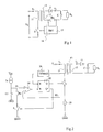
- Figure 1 shows a classic example of a switching regulator. This is a regulator called accumulation or "flyback".
- the first winding 11 is connected to a voltage source V1 by a power switch S.
- the secondary winding 12 is connected to the load R L by a diode D.
- a filtering capacitor C is connected in parallel to the load R L.
- the diode D is connected so that no current flows in the load when the primary winding 11 is connected to the voltage V1.
- the current I1 in the primary winding 11 increases from an initial value, as a function of the values of the voltage V1 and of the inductance presented by the winding 11. During this time, the current I2 in the secondary winding 12 is zero and energy accumulates in the core 13.
- the current I1 When the switch S is open, the current I1 is suddenly canceled and the energy which has just been accumulated in the core 13 is transferred to the winding 12.
- the current I2 suddenly reaches a peak value equal to the peak current reached by the current I1, multiplied by the ratio of the number of turns of the windings 11 and 12.
- the current I2 begins to decrease as a function of the inductance of the winding 12 and of the voltage across the terminals of the load R L.
- the switch S is closed again when the current I2 has reached a generally undetermined final value.
- This final value possibly zero for some time, determines the initial value from which the current I1 begins to grow.
- the amount of energy transferred from primary to secondary is a function of the switching cycle ratio of switch S, that is to say of the ratio between its closing time at each switching and the switching period.
- a resistor Rs is arranged in series with the winding 12.
- the voltage across the resistor Rs is supplied to a regulation circuit 15 which controls the switch S.
- This circuit of regulation filters the voltage across the resistor Rs to extract the average value which is compared to a set value.
- the duty cycle of switch S is adjusted so that the average voltage across the resistor Rs (therefore the average secondary current) tends towards the setpoint.
- a drawback of any switching regulator with galvanic isolation between primary and secondary, such as that of FIG. 1, stems from the fact that the quantity to be measured (current, voltage) is located at the secondary while the element which makes it possible to adjust this quantity, the power switch S, is found in the primary.
- the quantity to be measured current, voltage
- the power switch S is found in the primary.
- dotted lines 16 it is necessary to provide galvanic isolation in the regulation circuit 15, between the part measuring the voltage across the resistor Rs and the part which controls the switch S.
- This isolation is carried out , for example, using a transformer or an opto-coupler.
- the use of a transformer is expensive and cumbersome while the use of an opto-coupler is expensive and unreliable over time (a large number of failures in current regulators comes from opto-couplers).
- An object of the present invention is to provide a switching current regulator whose regulation circuit is entirely on the side of the power switch, that is to say that it is not connected to the secondary and therefore does not require an isolation element.
- This object is achieved by using a regulator of the type of FIG. 1 in a particular operating mode, called self-oscillating, where the power switch is closed as soon as the current at the secondary is canceled.
- the current in the primary winding is measured and its peak value is adjusted to a reference value (which is obtained by opening the power switch when the current in the primary winding reaches this reference value).
- one aspect of the invention is to vary the reference value in the direction of the duty cycle.
- the invention relates more particularly to a switching current regulator of the storage type, comprising first and second coupled windings, and means for connecting the first winding to a voltage source as soon as the windings are demagnetized.
- the regulator further comprises a sensor of the current flowing in the first winding; means for disconnecting the first winding from the voltage source when the current in the first winding reaches a reference value; and means for varying the reference value in the direction of the duty cycle.
- a power switch connects the first winding to the voltage source with the duty cycle.
- a diode prevents current from flowing through the second winding when the first winding is connected to the voltage source.
- a demagnetization detector closes the switch when the current in the second winding is canceled. The switch is open when the current in the first winding reaches said reference value.
- the reference value corresponds to a reference voltage across a capacitor biased by a reference current source and discharged through a resistor switched in phase opposition with respect to said switch. power.
- the regulator comprises a comparator receiving the output of the current sensor and the reference voltage, and a flip-flop whose direct output controls the switch, whose complementary output controls the switching of the resistance , whose a reset input is controlled by the demagnetization detector, and a reset input is controlled by the comparator.
- a current sensor 20 detects, according to the invention, the current in the primary winding 11 of a converter of the type of FIG. 1.
- This sensor 20 is, for example, a simple resistance of low value disposed, as shown, between the power switch S and the negative terminal of the voltage source V1, here the ground GND.
- Current information denoted KI1, can also be provided in many other ways. For example, in the case where the power switch S is a vertical MOS transistor consisting of a large number of cells in parallel, the current information can be obtained from the current flowing in a small number of cells identical to those of the power MOS transistor.
- the switch S is controlled by the non-inverted output Q of a flip-flop 22 of RS type whose zero-setting input "R" receives the output of a comparator 24 which compares the current information KI1 with a reference voltage Vr.
- the input for setting to "S" of the flip-flop 22 receives the output of a demagnetization detection circuit 26, an example of which is described later in relation to FIG. 4. This detection circuit is used to operate the regulator in "self-oscillating" mode, essential mode to obtain a regulation of the average current at the secondary using a current measurement at the primary.
- FIG. 3 represents an example of the shape of the control signal of the switch S, of the reference voltage Vr, of the current information KI1, and of the current I2 in the secondary winding 12.
- the reference voltage Vr has been shown with a slight variation, the origin of which will be described later in relation to elements not yet described in FIG. 4.
- the current I1 When the switch S is closed, the current I1, and therefore the current information KI1, increases regularly essentially as a function of the voltage V1 and of the inductance of the winding 11. During this time, the current I2 is zero .
- the comparator 24 sets the flip-flop 22 to zero, which opens the switch S.
- the current I1 which has just reached its peak value I 1p , is abruptly canceled while the current I2 suddenly reaches its peak value I 2p which is equal to the peak current I 1p multiplied by the ratio n of the number of turns of the windings 11 and 12.
- the peak value I 1p is fixed at Vr / K and the peak value I 2p at nVr / K.
- the current I2 decreases regularly, essentially as a function of the voltage at the terminals of the load R L and of the inductance of the winding 12.
- the circuit demagnetization detection 26 sets the flip-flop 22 to one, which closes the switch S, and so on.
- This operating mode where the switch S is closed as soon as the current I2 at the secondary is canceled, is said to be "self-oscillating".
- the peak value I 1p of the current I1 is reached in a constant duration after each closing of the switch S.
- the time for canceling the current I2 varies in the opposite direction to the voltage across the load R L.
- the lower this voltage the longer the demagnetization time, and the lower the switching duty cycle r of the switch S.
- the average value I 2m increases with the decrease in the voltage across the load.
- the reference voltage Vr is collected across the terminals of a capacitor Cr, one terminal of which is connected to ground GND and the other to a supply voltage Vcc by a current source Ir.
- voltage Vcc is a direct supply voltage of the regulation circuit which is obtained from the voltage V1.
- the voltage Vr is also connected to ground GND via a resistor Rr arranged in series with a switch S1.
- This switch S1 is controlled by an inverted output Q * of the flip-flop 22. Thus, the switch S1 is switched with a duty cycle of 1-r.
- switch S1 When switch S is closed, switch S1 is open.
- the current source Ir charges the capacitor Cr and the voltage Vr tends towards Vcc.
- switch S1 When switch S is open, switch S1 is closed. Then, the resistance Rr derives part of the current from the source Ir and the voltage Vr tends towards a value RrIr.
- the charge and discharge time constants of the capacitance Cr are chosen to be high with respect to the switching period of the switch S.
- I 2m nRrIr / 2K, which is a constant value that can be set by adjusting any of the Ir, Rr or K values.
- FIG. 4 represents an example of a demagnetization detection circuit 26 which can be used in the regulator of FIG. 2. It comprises a PNP transistor Q1 whose emitter is connected to the voltage Vcc by a resistor R1 and whose collector is connected to GND ground. The base of transistor Q1 is connected to the connection point between switch S and winding 11 by a capacitor C1. A resistor R2 connects the base of the transistor Q1 to the voltage Vcc. The detection signal is taken from the emitter of transistor Q1 and inverted (40) before being supplied to flip-flop 22.
- the capacitor C1 While the switch S is closed, the capacitor C1 is positively charged on the side of the base of the transistor Q1 at the voltage Vcc.
- the switch S When the switch S is open, the voltage across the winding 11 reverses and starts to charge negatively the capacity C1 by the resistance R2.
- the current I2 When the current I2 is canceled, the voltage across the winding 11 is also canceled.
- the capacitor C1 is discharged through the base of the transistor Q1 and the resistor R1.
- the transistor Q1 which was previously blocked, becomes conductive and draws the output of the detection circuit to ground.
- FIG. 5 represents an embodiment of a converter according to the invention which can be easily integrated into logic boxes associated with vertical MOS transistors in MOS "Smart Power" technology.
- the switches S and S1 are MOS transistors.
- the winding 11, the current measurement resistor 20, and the capacitance Cr cannot be integrated and are connected to the integrated control circuit by respective pins 51, 52 and 53.
- the current Ir is supplied by a source comprising a transistor N channel MOS M1, a resistor R1, a voltage source Vref and an operational amplifier 55.
- the resistor R1 is connected between the drain of the transistor M1 and the voltage Vcc.
- the current Ir is taken from the source of the transistor M1.
- the amplifier 55 controls the gate of the transistor M1 and receives on its non-inverting input the drain voltage of the transistor M1.
- the voltage source Vref is connected between the inverting input of the amplifier 55 and the voltage Vcc.
- the current Ir is equal to Vref / R1.
- the exact values of the resistors R1 and Rr are difficult to determine, but what matters in this case is the ratio of the resistors R1 and Rr, which can be chosen with precision, because the resistors integrated on the same chip are paired.
Landscapes
- Engineering & Computer Science (AREA)
- Power Engineering (AREA)
- Dc-Dc Converters (AREA)
Abstract
Description
- La présente invention concerne un régulateur à découpage permettant de fournir un courant constant à une charge, par exemple une batterie, avec un rendement élevé. La présente invention vise plus particulièrement un régulateur de courant à découpage dont la charge doit être isolée de la source d'alimentation du régulateur, souvent le réseau 220 volts.
- La figure 1 représente un exemple classique de régulateur à découpage. Il s'agit ici d'un régulateur dit à accumulation ou "flyback". Pour isoler la charge RL de ce régulateur, on prévoit deux enroulements 11 et 12 couplés par un noyau magnétique 13, mais isolés galvaniquement. Le premier enroulement 11 est relié à une source de tension V₁ par un interrupteur de puissance S. Bien que les enroulements 11 et 12 ne constituent pas un transformateur (des courants ne circulent pas simultanément dans les deux enroulements), on utilisera quand même les termes "primaire" et "secondaire" pour simplifier la description. L'enroulement secondaire 12 est relié à la charge RL par une diode D. Une capacité de filtrage C est connectée en parallèle sur la charge RL. La diode D est connectée de manière qu'aucun courant ne circule dans la charge lorsque l'enroulement primaire 11 est connecté à la tension V₁.
- Lorsque l'interrupteur S est fermé, le courant I₁ dans l'enroulement primaire 11 augmente à partir d'une valeur initiale, en fonction des valeurs de la tension V₁ et de l'inductance présentée par l'enroulement 11. Pendant ce temps, le courant I₂ dans l'enroulement secondaire 12 est nul et de l'énergie s'accumule dans le noyau 13.
- Lorsque l'interrupteur S est ouvert, le courant I₁ s'annule brusquement et l'énergie qui vient d'être accumulée dans le noyau 13 est transférée vers l'enroulement 12. Le courant I₂ atteint brusquement une valeur crête égale au courant crête atteint par le courant I₁, multiplié par le rapport du nombre de spires des enroulements 11 et 12. Le courant I₂ se met à décroître en fonction de l'inductance de l'enroulement 12 et de la tension aux bornes de la charge RL.
- L'interrupteur S est de nouveau fermé alors que le courant I₂ a atteint une valeur finale généralement indéterminée. Cette valeur finale, éventuellement nulle depuis un certain temps, détermine la valeur initiale à partir de laquelle le courant I₁ se met à croître.
- La quantité d'énergie transférée du primaire vers le secondaire est fonction du rapport cyclique de commutation de l'interrupteur S, c'est-à-dire du rapport entre son temps de fermeture à chaque commutation et la période de commutation.
- Pour assurer une régulation du courant moyen dans la charge, une résistance Rs est disposée en série avec l'enroulement 12. La tension aux bornes de la résistance Rs est fournie à un circuit de régulation 15 qui commande l'interrupteur S. Ce circuit de régulation filtre la tension aux bornes de la résistance Rs pour en extraire la valeur moyenne qui est comparée à une valeur de consigne. Le rapport cyclique de l'interrupteur S est ajusté de manière que la tension moyenne aux bornes de la résistance Rs (donc le courant secondaire moyen) tende vers la consigne.
- Un inconvénient de tout régulateur à découpage à isolation galvanique entre primaire et secondaire, tel que celui de la figure 1, provient du fait que la grandeur à mesurer (courant, tension) se trouve au secondaire alors que l'élément qui permet d'ajuster cette grandeur, l'interrupteur de puissance S, se trouve au primaire. Comme cela est illustré par des pointillés 16, il est nécessaire de prévoir une isolation galvanique dans le circuit de régulation 15, entre la partie mesurant la tension aux bornes de la résistance Rs et la partie qui commande l'interrupteur S. Cette isolation est effectuée, par exemple, en utilisant un transformateur ou un opto-coupleur. L'utilisation d'un transformateur est coûteuse et encombrante tandis que l'utilisation d'un opto-coupleur est coûteuse et peu fiable dans le temps (un grand nombre de pannes dans des régulateurs actuels provient des opto-coupleurs).
- Bien entendu, on pourrait envisager de réguler le courant moyen dans l'enroulement primaire 11, mais cette solution entraîne une régulation de la puissance moyenne fournie à la charge RL et non de son courant moyen qui varie alors en fonction de la tension d'alimentation V₁ et de la tension de sortie aux bornes de la charge.
- Un objet de la présente invention est de prévoir un régulateur de courant à découpage dont le circuit de régulation se trouve entièrement du côté de l'interrupteur de puissance, c'est-à-dire qu'il n'est pas relié au secondaire et ne nécessite donc pas d'élément d'isolement.
- Cet objet est atteint en utilisant un régulateur du type de la figure 1 dans un mode de fonctionnement particulier, dit auto-oscillant, où l'interrupteur de puissance est fermé dès que le courant au secondaire s'annule. Le courant dans l'enroulement primaire est mesuré et on ajuste sa valeur crête à une valeur de référence (ce qui est obtenu en ouvrant l'interrupteur de puissance lorsque le courant dans l'enroulement primaire atteint cette valeur de référence).
- Cette seule mesure ne suffit pas car le rapport cyclique, et donc le courant moyen dans la charge au secondaire, dépend alors de la tension aux bornes de cette charge. Pour éviter cela, un aspect de l'invention est de faire varier la valeur de référence dans le sens du rapport cyclique.
- L'invention concerne plus particulièrement un régulateur de courant à découpage du type à accumulation, comprenant des premier et deuxième enroulements couplés, et des moyens pour connecter le premier enroulement à une source de tension dès que les enroulements sont démagnétisés. Le régulateur comprend en outre un capteur du courant circulant dans le premier enroulement ; des moyens pour déconnecter le premier enroulement de la source de tension quand le courant dans le premier enroulement atteint une valeur de référence ; et des moyens pour faire varier la valeur de référence dans le sens du rapport cyclique.
- Selon un mode de réalisation de la présente invention, un interrupteur de puissance connecte le premier enroulement à la source de tension avec le rapport cyclique. Une diode empêche un courant de circuler dans le deuxième enroulement lorsque le premier enroulement est connecté à la source de tension. Un détecteur de démagnétisation ferme l'interrupteur lorsque le courant dans le deuxième enroulement s'annule. L'interrupteur est ouvert lorsque le courant dans le premier enroulement atteint ladite valeur de référence.
- Selon un mode de réalisation de la présente invention, la valeur de référence correspond à une tension de référence aux bornes d'une capacité polarisée par une source de courant de référence et déchargée à travers une résistance commutée en opposition de phase par rapport audit interrupteur de puissance.
- Selon un mode de réalisation de la présente invention, le régulateur comprend un comparateur recevant la sortie du capteur de courant et la tension de référence, et une bascule dont une sortie directe commande l'interrupteur, dont une sortie complémentaire commande la commutation de la résistance, dont une entrée de mise à un est commandée par le détecteur de démagnétisation, et dont une entrée de mise à zéro est commandée par le comparateur.
- Ces objets, caractéristiques, avantages ainsi que d'autres de la présente invention seront exposés plus en détail dans la description suivante de modes de réalisation particuliers faite à titre non limitatif à l'aide des figures jointes parmi lesquelles :
- la figure 1, précédemment décrite, représente un exemple classique de régulateur à découpage dit à accumulation ;
- la figure 2 représente un mode de réalisation selon la présente invention d'un circuit de commande d'interrupteur de puissance dans un régulateur de courant à découpage ;
- la figure 3 représente des allures de signaux du circuit de la figure 2 ;
- la figure 4 représente un exemple classique de circuit de détection de démagnétisation que l'on utilise dans certains convertisseurs à accumulation ; et
- la figure 5 représente un mode de réalisation facilement intégrable en technologie "Smart Power" du circuit de la figure 2.
- Dans la figure 2, un capteur de courant 20 détecte, selon l'invention, le courant dans l'enroulement primaire 11 d'un convertisseur du type de la figure 1. Ce capteur 20 est, par exemple, une simple résistance de faible valeur disposée, comme cela est représenté, entre l'interrupteur de puissance S et la borne négative de la source de tension V₁, ici la masse GND. L'information de courant, notée KI₁, peut également être fournie de nombreuses autres manières. Par exemple, dans le cas où l'interrupteur de puissance S est un transistor MOS vertical constitué d'un grand nombre de cellules en parallèle, l'information de courant pourra être obtenue à partir du courant circulant dans un petit nombre de cellules identiques à celles du transistor MOS de puissance.
- L'interrupteur S est commandé par la sortie non-inversée Q d'une bascule 22 de type RS dont l'entrée de mise à zéro "R" reçoit la sortie d'un comparateur 24 qui compare l'information de courant KI₁ à une tension de référence Vr. L'entrée de mise à un "S" de la bascule 22 reçoit la sortie d'un circuit de détection de démagnétisation 26, dont un exemple est décrit ultérieurement en relation avec la figure 4. Ce circuit de détection sert à faire fonctionner le régulateur en mode "auto-oscillant", mode indispensable pour obtenir une régulation du courant moyen au secondaire à l'aide d'une mesure du courant au primaire.
- La figure 3 représente un exemple d'allure du signal de commande de l'interrupteur S, de la tension de référence Vr, de l'information de courant KI₁, et du courant I₂ dans l'enroulement secondaire 12. La tension de référence Vr a été représentée avec une légère variation dont l'origine sera décrite ultérieurement en relation avec des éléments non encore décrits de la figure 4.
- Quand l'interrupteur S est fermé, le courant I₁, et donc l'information de courant KI₁, croissent régulièrement essentiellement en fonction de la tension V₁ et de l'inductance de l'enroulement 11. Pendant ce temps, le courant I₂ est nul.
- Quand l'information KI₁ atteint la valeur Vr, le comparateur 24 met la bascule 22 à zéro, ce qui ouvre l'interrupteur S. Le courant I₁, qui vient d'atteindre sa valeur crête I1p, s'annule brusquement tandis que le courant I₂ atteint brusquement sa valeur crête I2p qui est égale au courant crête I1p multiplié par le rapport n du nombre de spires des enroulements 11 et 12. Ainsi, la valeur crête I1p est fixée à Vr/K et la valeur crête I2p à nVr/K. Le courant I₂ décroît régulièrement, essentiellement en fonction de la tension aux bornes de la charge RL et de l'inductance de l'enroulement 12.
- Quand le courant I₂ s'annule, c'est-à-dire quand le noyau 13 des enroulements 11 et 12 est démagnétisé, le circuit de détection de démagnétisation 26 met la bascule 22 à un, ce qui ferme l'interrupteur S, et ainsi de suite. Ce mode de fonctionnement, où l'interrupteur S est refermé dès que le courant I₂ au secondaire s'annule, est dit "auto-oscillant".
- Dans ce mode de fonctionnement auto-oscillant, et en supposant que la valeur de la tension aux bornes de la charge RL ne varie pas significativement pendant un cycle de commutation de l'interrupteur S (ce qui est le cas d'une batterie), la valeur moyenne du courant I₂ s'exprime par

- En supposant que les tensions V₁ et Vr sont constantes, la valeur crête I1p du courant I₁ est atteinte en une durée constante après chaque fermeture de l'interrupteur S. Le temps d'annulation du courant I₂ varie dans le sens inverse de la tension aux bornes de la charge RL. Plus cette tension est faible, plus le temps de démagnétisation est long, et plus le rapport cyclique r de commutation de l'interrupteur S est faible. Alors, d'après la relation (1), la valeur moyenne I2m augmente avec la diminution de la tension aux bornes de la charge. On obtient un effet de régulation de puissance fournie à la charge RL et non de régulation du courant dans la charge RL.
- Pour obtenir une régulation du courant dans la charge RL, il est prévu, selon un aspect de l'invention, de faire varier la tension de référence Vr dans le même sens que le rapport cyclique r, par exemple proportionnellement à 1/(1-r).
- Pour cela, dans la figure 2, la tension de référence Vr est recueillie aux bornes d'une capacité Cr dont une borne est connectée à la masse GND et l'autre à une tension d'alimentation Vcc par une source de courant Ir. La tension Vcc est une tension continue d'alimentation du circuit de régulation qui est obtenue à partir de la tension V₁. La tension Vr est également reliée à la masse GND par l'intermédiaire d'une résistance Rr disposée en série avec un interrupteur S1. Cet interrupteur S1 est commandé par une sortie inversée Q* de la bascule 22. Ainsi, l'interrupteur S1 est commuté avec un rapport cyclique de 1-r.
- Quand l'interrupteur S est fermé, l'interrupteur S1 est ouvert. La source de courant Ir charge la capacité Cr et la tension Vr tend vers Vcc. Lorsque l'interrupteur S est ouvert, l'interrupteur S1 est fermé. Alors, la résistance Rr dérive une partie du courant de la source Ir et la tension Vr tend vers une valeur RrIr.
- En pratique, les constantes de temps de charge et de décharge de la capacité Cr sont choisies élevées par rapport à la période de commutation de l'interrupteur S. Ainsi, la tension Vr est pratiquement constante, et elle s'établit à une valeur

- La valeur crête du courant I₁ est fixée à

- En combinant les relations (1) et (2), on obtient :

- La figure 4 représente un exemple de circuit de détection de démagnétisation 26 que l'on peut utiliser dans le régulateur de la figure 2. Il comprend un transistor PNP Q1 dont l'émetteur est relié à la tension Vcc par une résistance R1 et dont le collecteur est relié à la masse GND. La base du transistor Q1 est reliée au point de connexion entre l'interrupteur S et l'enroulement 11 par une capacité C1. Une résistance R2 relie la base du transistor Q1 à la tension Vcc. Le signal de détection est prélevé sur l'émetteur du transistor Q1 et inversé (40) avant d'être fourni à la bascule 22.
- Pendant que l'interrupteur S est fermé, la capacité C1 est chargée positivement du côté de la base du transistor Q1 à la tension Vcc. Lorsque l'interrupteur S est ouvert, la tension aux bornes de l'enroulement 11 s'inverse et se met à charger négativement la capacité C1 par la résistance R2. Au moment où le courant I₂ s'annule, la tension aux bornes de l'enroulement 11 s'annule également. Alors, la capacité C1 se décharge par la base du transistor Q1 et la résistance R1. Le transistor Q1, qui était jusque là bloqué, devient conducteur et tire la sortie du circuit de détection vers la masse.
- La figure 5 représente un mode de réalisation de convertisseur selon l'invention facilement intégrable dans des caissons logiques associés à des transistors MOS verticaux en technologie MOS "Smart Power". Les interrupteurs S et S1 sont des transistors MOS. L'enroulement 11, la résistance de mesure de courant 20, et la capacité Cr ne peuvent être intégrés et sont reliés au circuit de commande intégré par des broches respectives 51, 52 et 53. Le courant Ir est fourni par une source comprenant un transistor MOS M1 à canal N, une résistance R1, une source de tension Vref et un amplificateur opérationnel 55. La résistance R1 est reliée entre le drain du transistor M1 et la tension Vcc. Le courant Ir est prélevé sur la source du transistor M1. L'amplificateur 55 commande la grille du transistor M1 et reçoit sur son entrée non-inverseuse la tension de drain du transistor M1. La source de tension Vref est reliée entre l'entrée inverseuse de l'amplificateur 55 et la tension Vcc.
- Avec cette configuration, le courant Ir est égal à Vref/R1. Les valeurs exactes des résistances R1 et Rr sont difficiles à déterminer, mais ce qui importe dans ce cas est le rapport des résistances R1 et Rr, qui peut être choisi avec précision, car les résistances intégrées sur une même puce sont appariées.
Claims (4)
- Régulateur de courant à découpage du type à accumulation comprenant :- des premier (11) et deuxième (12) enroulements couplés ;- des moyens (S, 26) pour connecter le premier enroulement à une source de tension (V₁) dès que les enroulements sont démagnétisés ; caractérisé en ce qu'il comprend :- un capteur (20) du courant (I₁) circulant dans le premier enroulement ;- des moyens (24, S) pour déconnecter le premier enroulement de la source de tension quand le courant dans le premier enroulement atteint une valeur de référence (Vr/K), d'où il résulte que le premier enroulement est commuté avec un rapport cyclique (r) ; et- des moyens (Ir, Cr, S1, Rr) pour faire varier la valeur de référence dans le sens dudit rapport cyclique.
- Régulateur de courant selon la revendication 1, caractérisé en ce qu'il comprend :- un interrupteur de puissance (S) connectant le premier enroulement (11) à la source de tension (V₁) avec ledit rapport cyclique ;- des moyens (D) pour empêcher un courant de circuler dans le deuxième enroulement (12) lorsque le premier enroulement est connecté à la source de tension ;- un détecteur de démagnétisation (26) pour fermer l'interrupteur lorsque le courant dans le deuxième enroulement s'annule ; et- des moyens (24) pour ouvrir l'interrupteur lorsque le courant dans le premier enroulement atteint ladite valeur de référence.
- Régulateur de courant selon la revendication 2, caractérisé en ce que ladite valeur de référence correspond à une tension de référence (Vr) aux bornes d'une capacité (Cr) polarisée par une source de courant de référence (Ir) et déchargée à travers une résistance (Rr) commutée en opposition de phase par rapport audit interrupteur de puissance.
- Régulateur de courant selon la revendication 3, caractérisé en ce qu'il comprend :- un comparateur (24) recevant la sortie (KI₁) du capteur de courant et la tension de référence (Vr) ; et- une bascule (22) dont une sortie directe (Q) commande ledit interrupteur (S), dont une sortie complémentaire (Q*) commande la commutation de ladite résistance (Rr), dont une entrée de mise à un (S) est commandée par le détecteur de démagnétisation, et dont une entrée de mise à zéro (R) est commandée par le comparateur.
Applications Claiming Priority (2)
| Application Number | Priority Date | Filing Date | Title |
|---|---|---|---|
| FR9411973A FR2725324B1 (fr) | 1994-09-30 | 1994-09-30 | Regulateur de courant a decoupage |
| FR9411973 | 1994-09-30 |
Publications (2)
| Publication Number | Publication Date |
|---|---|
| EP0704956A1 true EP0704956A1 (fr) | 1996-04-03 |
| EP0704956B1 EP0704956B1 (fr) | 1998-12-16 |
Family
ID=9467643
Family Applications (1)
| Application Number | Title | Priority Date | Filing Date |
|---|---|---|---|
| EP95410115A Expired - Lifetime EP0704956B1 (fr) | 1994-09-30 | 1995-09-26 | Régulateur de courant à découpage |
Country Status (5)
| Country | Link |
|---|---|
| US (1) | US5729443A (fr) |
| EP (1) | EP0704956B1 (fr) |
| JP (1) | JP2860304B2 (fr) |
| DE (1) | DE69506656T2 (fr) |
| FR (1) | FR2725324B1 (fr) |
Cited By (4)
| Publication number | Priority date | Publication date | Assignee | Title |
|---|---|---|---|---|
| WO2008097305A3 (fr) * | 2007-02-08 | 2008-10-02 | Linear Techn Inc | Régulateur adaptatif de courant de sortie pour des circuits de commutation |
| WO2011045097A1 (fr) * | 2009-09-21 | 2011-04-21 | Osram Gesellschaft mit beschränkter Haftung | Circuiterie pour faire fonctionner au moins une diode électroluminescente (del) |
| CN104302053A (zh) * | 2014-10-09 | 2015-01-21 | 泉芯电子技术(深圳)有限公司 | Led恒流源输出检测控制电路及其控制方法 |
| CN104754824A (zh) * | 2015-02-26 | 2015-07-01 | 泉芯电子技术(深圳)有限公司 | 一种led恒流源及其去磁时间检测方法 |
Families Citing this family (39)
| Publication number | Priority date | Publication date | Assignee | Title |
|---|---|---|---|---|
| DE19818315C1 (de) * | 1998-04-23 | 1999-09-16 | Siemens Ag | Einrichtung zum ratiometrischen Messen von Sensorsignalen |
| AT408294B (de) * | 1998-09-30 | 2001-10-25 | Siemens Ag Oesterreich | Sperrwandler |
| JP3829534B2 (ja) | 1999-05-26 | 2006-10-04 | 松下電工株式会社 | 放電灯点灯装置 |
| TW459438B (en) * | 1999-09-17 | 2001-10-11 | Koninkl Philips Electronics Nv | Multimode switched-mode power supply |
| DE10018229B4 (de) * | 2000-12-04 | 2005-05-19 | Friwo Gerätebau Gmbh | Verfahren zur Regulierung des Ausgangsstroms und/oder der Ausgangsspannung eines Schaltnetzteils |
| DE10040413B4 (de) * | 2000-08-18 | 2006-11-09 | Infineon Technologies Ag | Schaltungsanordnung zur Erzeugung eines Schaltsignals für ein stromgesteuertes Schaltnetzteil |
| EP1215808B1 (fr) * | 2000-12-13 | 2011-05-11 | Semiconductor Components Industries, LLC | Circuit d'alimentation de puissance et procédé associé pour la detection de la démagnetisation de l'alimentation de puissance |
| US6781357B2 (en) * | 2001-09-27 | 2004-08-24 | Power Integrations, Inc. | Method and apparatus for maintaining a constant load current with line voltage in a switch mode power supply |
| US6686781B2 (en) * | 2002-04-12 | 2004-02-03 | Itt Manufacturing Enterprises, Inc. | Timing control circuit |
| WO2004054080A1 (fr) * | 2002-12-12 | 2004-06-24 | Sanken Electric Co., Ltd. | Appareil d'alimentation electrique en courant continu |
| DE10331866B4 (de) * | 2003-07-14 | 2008-11-13 | Minebea Co., Ltd. | Einrichtung zur Steuerung einer Spulenanordnung mit elektrisch variierbarer Induktivität, sowie Schaltnetzteil |
| US7568117B1 (en) | 2005-10-03 | 2009-07-28 | Zilker Labs, Inc. | Adaptive thresholding technique for power supplies during margining events |
| KR101309293B1 (ko) | 2007-03-28 | 2013-09-16 | 페어차일드코리아반도체 주식회사 | 스위칭 모드 파워 서플라이 및 그 구동 방법 |
| KR101365752B1 (ko) * | 2007-04-19 | 2014-02-21 | 페어차일드코리아반도체 주식회사 | 스위칭 모드 파워 서플라이 및 이를 위한 스위치 |
| US7898823B2 (en) * | 2007-05-08 | 2011-03-01 | Leadtrend Technology Corp. | Quasi-resonant fly-back converter without auxiliary winding |
| US8040699B2 (en) * | 2007-07-09 | 2011-10-18 | Active-Semi, Inc. | Secondary side constant voltage and constant current controller |
| KR101468719B1 (ko) * | 2008-03-12 | 2014-12-05 | 페어차일드코리아반도체 주식회사 | 전력 변환기 및 그 구동 방법 |
| JP5149686B2 (ja) * | 2008-04-24 | 2013-02-20 | パナソニック株式会社 | 電力変換装置及びそれを用いた放電灯点灯装置、並びに車両用前照灯装置 |
| US8179699B2 (en) * | 2008-12-31 | 2012-05-15 | Stmicroelectronics S.R.L. | Method for controlling a switching regulator and related switching regulator |
| US8514595B1 (en) | 2009-08-04 | 2013-08-20 | Qualcomm Incorporated | Switching power supply operation with reduced harmonic interference |
| US8299730B2 (en) | 2010-02-09 | 2012-10-30 | Power Integrations, Inc. | Integrated on-time extension for non-dissipative bleeding in a power supply |
| US8553439B2 (en) * | 2010-02-09 | 2013-10-08 | Power Integrations, Inc. | Method and apparatus for determining zero-crossing of an AC input voltage to a power supply |
| IT1400266B1 (it) | 2010-05-31 | 2013-05-24 | St Microelectronics Srl | Circuito integrato di controllo per un transistor di potenza di un regolatore di corrente a commutazione. |
| US8531131B2 (en) * | 2010-09-22 | 2013-09-10 | Osram Sylvania Inc. | Auto-sensing switching regulator to drive a light source through a current regulator |
| CN102064703B (zh) * | 2010-11-04 | 2013-11-06 | 成都芯源系统有限公司 | 开关电源恒流输出控制装置和方法 |
| JP5977738B2 (ja) * | 2011-04-25 | 2016-08-24 | ローム株式会社 | スイッチング電源装置及びこれを用いた電子機器 |
| KR101337349B1 (ko) * | 2012-03-21 | 2013-12-06 | 주식회사 동운아나텍 | 조명 구동 장치 및 그 방법 |
| US9287798B2 (en) | 2012-12-06 | 2016-03-15 | Stmicroelectronics, Inc. | High power factor primary regulated offline LED driver |
| CN103066869A (zh) * | 2012-12-24 | 2013-04-24 | 泉芯电子技术(深圳)有限公司 | 一种基于三极管的去磁时间检测电路 |
| US9042127B2 (en) | 2013-03-15 | 2015-05-26 | Infineon Technologies Austria Ag | LED power supply |
| CN103760408B (zh) * | 2014-01-26 | 2017-02-15 | 矽力杰半导体技术(杭州)有限公司 | 过零检测电路 |
| US9214862B2 (en) * | 2014-04-17 | 2015-12-15 | Philips International, B.V. | Systems and methods for valley switching in a switching power converter |
| US9455636B2 (en) * | 2014-12-16 | 2016-09-27 | Stmicroelectronics S.R.L. | Control method and device employing primary side regulation in a quasi-resonant AC/DC flyback converter |
| US9520796B2 (en) | 2015-03-06 | 2016-12-13 | Stmicroelectronics S.R.L. | Control method and device for quasi-resonant high-power-factor flyback converter |
| US9621029B2 (en) | 2015-03-18 | 2017-04-11 | Stmicroelectronics S.R.L. | Method and device for high-power-factor flyback converter |
| US10714960B2 (en) * | 2015-12-22 | 2020-07-14 | Intel Corporation | Uniform wireless charging device |
| US9913329B2 (en) | 2016-06-30 | 2018-03-06 | Stmicroelectronics S.R.L. | Control method and device employing primary side regulation in a quasi-resonant AC/DC flyback converter without analog divider and line-sensing |
| CN107889321B (zh) * | 2016-09-29 | 2020-06-16 | 卡任特照明解决方案有限公司 | 驱动电路 |
| IT201700022236A1 (it) * | 2017-02-28 | 2018-08-28 | St Microelectronics Srl | Circuito di controllo, alimentatore, apparecchiatura e procedimento corrispondenti |
Citations (3)
| Publication number | Priority date | Publication date | Assignee | Title |
|---|---|---|---|---|
| EP0335194A1 (fr) * | 1988-03-25 | 1989-10-04 | Siemens Aktiengesellschaft | Procédé de limitation du courant de sortie d'une alimentation en courant |
| US4939632A (en) * | 1989-02-14 | 1990-07-03 | U.S. Philips Corporation | Power supply circuit |
| EP0605057A2 (fr) * | 1992-12-30 | 1994-07-06 | Koninklijke Philips Electronics N.V. | Circuit d'alimentation à découpage et circuit de contrôle destiné à être utilisé dans un tel circuit d'alimentation |
Family Cites Families (6)
| Publication number | Priority date | Publication date | Assignee | Title |
|---|---|---|---|---|
| US4600984A (en) * | 1984-03-02 | 1986-07-15 | Itzchak Cohen | Two quadrant power modulator |
| JPH01500080A (ja) * | 1986-07-03 | 1989-01-12 | メルヒアー・アクチエンゲゼルシヤフト | 接続調整器の作動方法およびこの方法によつて作動する接続調整器 |
| ES2048806T3 (es) * | 1989-09-29 | 1994-04-01 | Siemens Ag | Disposicion de circuito para una fuente de alimentacion de conexion de convertidor de bloqueo regulada. |
| FR2674074A1 (fr) * | 1991-03-14 | 1992-09-18 | Telemecanique | Procede et dispositif pour la protection contre les surcharges, d'un circuit de conversion electrique. |
| GB9116616D0 (en) * | 1991-08-01 | 1991-09-18 | Thomson Consumer Electronics | Switched mode power supply with startup precharge |
| JP2733004B2 (ja) * | 1993-06-18 | 1998-03-30 | 株式会社日吉電機製作所 | スイッチング電源の制御回路 |
-
1994
- 1994-09-30 FR FR9411973A patent/FR2725324B1/fr not_active Expired - Fee Related
-
1995
- 1995-09-26 EP EP95410115A patent/EP0704956B1/fr not_active Expired - Lifetime
- 1995-09-26 DE DE69506656T patent/DE69506656T2/de not_active Expired - Fee Related
- 1995-09-27 US US08/534,497 patent/US5729443A/en not_active Expired - Lifetime
- 1995-09-29 JP JP7251678A patent/JP2860304B2/ja not_active Expired - Fee Related
Patent Citations (3)
| Publication number | Priority date | Publication date | Assignee | Title |
|---|---|---|---|---|
| EP0335194A1 (fr) * | 1988-03-25 | 1989-10-04 | Siemens Aktiengesellschaft | Procédé de limitation du courant de sortie d'une alimentation en courant |
| US4939632A (en) * | 1989-02-14 | 1990-07-03 | U.S. Philips Corporation | Power supply circuit |
| EP0605057A2 (fr) * | 1992-12-30 | 1994-07-06 | Koninklijke Philips Electronics N.V. | Circuit d'alimentation à découpage et circuit de contrôle destiné à être utilisé dans un tel circuit d'alimentation |
Cited By (5)
| Publication number | Priority date | Publication date | Assignee | Title |
|---|---|---|---|---|
| WO2008097305A3 (fr) * | 2007-02-08 | 2008-10-02 | Linear Techn Inc | Régulateur adaptatif de courant de sortie pour des circuits de commutation |
| US7639517B2 (en) | 2007-02-08 | 2009-12-29 | Linear Technology Corporation | Adaptive output current control for switching circuits |
| WO2011045097A1 (fr) * | 2009-09-21 | 2011-04-21 | Osram Gesellschaft mit beschränkter Haftung | Circuiterie pour faire fonctionner au moins une diode électroluminescente (del) |
| CN104302053A (zh) * | 2014-10-09 | 2015-01-21 | 泉芯电子技术(深圳)有限公司 | Led恒流源输出检测控制电路及其控制方法 |
| CN104754824A (zh) * | 2015-02-26 | 2015-07-01 | 泉芯电子技术(深圳)有限公司 | 一种led恒流源及其去磁时间检测方法 |
Also Published As
| Publication number | Publication date |
|---|---|
| FR2725324B1 (fr) | 1996-12-20 |
| US5729443A (en) | 1998-03-17 |
| JPH08182314A (ja) | 1996-07-12 |
| DE69506656D1 (de) | 1999-01-28 |
| EP0704956B1 (fr) | 1998-12-16 |
| FR2725324A1 (fr) | 1996-04-05 |
| DE69506656T2 (de) | 1999-05-20 |
| JP2860304B2 (ja) | 1999-02-24 |
Similar Documents
| Publication | Publication Date | Title |
|---|---|---|
| EP0704956B1 (fr) | Régulateur de courant à découpage | |
| FR2724502A1 (fr) | Appareil d'egalisation de la charge de batteries connectees en serie | |
| EP1334551A1 (fr) | Convertisseur de tension a circuit de commande autooscillant | |
| FR2476929A1 (fr) | Circuit de charge d'une pile et d'alimentation en energie electrique a partir de l'energie solaire | |
| FR2768527A1 (fr) | Regulateur de tension | |
| FR3001089A1 (fr) | Equilibrage de charge dans une batterie electrique | |
| EP0454597A1 (fr) | Circuit de commande de grille par impulsion avec securité de court-circuit | |
| FR2783053A1 (fr) | Procede de diagnostic d'un court-circuit sur un organe de reglage capacitif | |
| FR2583236A1 (fr) | Dispositif electrique de puissance " intelligent " a circuit integre monolithique | |
| EP1040559B1 (fr) | Procede de commande d'un convertisseur de tension continu-continu a stockage inductif | |
| FR2863115A1 (fr) | Interrupteur de circuit en cas de defaut a la terre. | |
| FR2896211A1 (fr) | Dispositif de gestion electrique pour alimentation electrique de vehicule | |
| FR2608858A1 (fr) | Procede et dispositif pour la connexion d'une batterie de stockage d'energie a un convertisseur d'ascenseur | |
| EP0772287A1 (fr) | Alimentation à découpage à correction de facteur de puissance | |
| FR2743953A1 (fr) | Circuit d'alimentation a condensateur de stockage | |
| EP0530061B1 (fr) | Circuit régulateur de la tension de charge d'une batterie par un alternateur | |
| FR2842664A1 (fr) | Chargeur pour batterie | |
| EP4216564B1 (fr) | Calibration d'un pixel numérique iwr d'imageur | |
| FR2490895A1 (fr) | Circuit d'entretien pour oscillateur a faible consommation de courant | |
| EP4639705A1 (fr) | Installation solaire à panneau photovoltaïque | |
| JP4380091B2 (ja) | 二次電池の充電装置 | |
| FR2461395A1 (fr) | Convertisseur de tension alternative en tension continue | |
| FR3055752B1 (fr) | Circuit de transmission d'energie electrique | |
| FR2481530A1 (fr) | Procede et dispositif de production d'impulsions electriques pour le pompage d'un laser | |
| FR2659507A1 (fr) | Convertisseur de courant continu en courant continu. |
Legal Events
| Date | Code | Title | Description |
|---|---|---|---|
| PUAI | Public reference made under article 153(3) epc to a published international application that has entered the european phase |
Free format text: ORIGINAL CODE: 0009012 |
|
| AK | Designated contracting states |
Kind code of ref document: A1 Designated state(s): DE FR GB IT |
|
| 17P | Request for examination filed |
Effective date: 19960909 |
|
| GRAG | Despatch of communication of intention to grant |
Free format text: ORIGINAL CODE: EPIDOS AGRA |
|
| 17Q | First examination report despatched |
Effective date: 19971127 |
|
| GRAG | Despatch of communication of intention to grant |
Free format text: ORIGINAL CODE: EPIDOS AGRA |
|
| GRAH | Despatch of communication of intention to grant a patent |
Free format text: ORIGINAL CODE: EPIDOS IGRA |
|
| GRAH | Despatch of communication of intention to grant a patent |
Free format text: ORIGINAL CODE: EPIDOS IGRA |
|
| GRAA | (expected) grant |
Free format text: ORIGINAL CODE: 0009210 |
|
| AK | Designated contracting states |
Kind code of ref document: B1 Designated state(s): DE FR GB IT |
|
| REF | Corresponds to: |
Ref document number: 69506656 Country of ref document: DE Date of ref document: 19990128 |
|
| RAP4 | Party data changed (patent owner data changed or rights of a patent transferred) |
Owner name: STMICROELECTRONICS S.A. |
|
| ITF | It: translation for a ep patent filed | ||
| GBT | Gb: translation of ep patent filed (gb section 77(6)(a)/1977) |
Effective date: 19990211 |
|
| PLBE | No opposition filed within time limit |
Free format text: ORIGINAL CODE: 0009261 |
|
| STAA | Information on the status of an ep patent application or granted ep patent |
Free format text: STATUS: NO OPPOSITION FILED WITHIN TIME LIMIT |
|
| 26N | No opposition filed | ||
| REG | Reference to a national code |
Ref country code: GB Ref legal event code: IF02 |
|
| PGFP | Annual fee paid to national office [announced via postgrant information from national office to epo] |
Ref country code: DE Payment date: 20040923 Year of fee payment: 10 |
|
| PGFP | Annual fee paid to national office [announced via postgrant information from national office to epo] |
Ref country code: FR Payment date: 20050823 Year of fee payment: 11 |
|
| PGFP | Annual fee paid to national office [announced via postgrant information from national office to epo] |
Ref country code: GB Payment date: 20050921 Year of fee payment: 11 |
|
| PG25 | Lapsed in a contracting state [announced via postgrant information from national office to epo] |
Ref country code: IT Free format text: LAPSE BECAUSE OF NON-PAYMENT OF DUE FEES;WARNING: LAPSES OF ITALIAN PATENTS WITH EFFECTIVE DATE BEFORE 2007 MAY HAVE OCCURRED AT ANY TIME BEFORE 2007. THE CORRECT EFFECTIVE DATE MAY BE DIFFERENT FROM THE ONE RECORDED. Effective date: 20050926 |
|
| PG25 | Lapsed in a contracting state [announced via postgrant information from national office to epo] |
Ref country code: DE Free format text: LAPSE BECAUSE OF NON-PAYMENT OF DUE FEES Effective date: 20060401 |
|
| GBPC | Gb: european patent ceased through non-payment of renewal fee |
Effective date: 20060926 |
|
| REG | Reference to a national code |
Ref country code: FR Ref legal event code: ST Effective date: 20070531 |
|
| PG25 | Lapsed in a contracting state [announced via postgrant information from national office to epo] |
Ref country code: GB Free format text: LAPSE BECAUSE OF NON-PAYMENT OF DUE FEES Effective date: 20060926 |
|
| PG25 | Lapsed in a contracting state [announced via postgrant information from national office to epo] |
Ref country code: FR Free format text: LAPSE BECAUSE OF NON-PAYMENT OF DUE FEES Effective date: 20061002 |