EP0704994A1 - Circuit photodétecteur avec entrée accordé à amortissement actif - Google Patents
Circuit photodétecteur avec entrée accordé à amortissement actif Download PDFInfo
- Publication number
- EP0704994A1 EP0704994A1 EP95306639A EP95306639A EP0704994A1 EP 0704994 A1 EP0704994 A1 EP 0704994A1 EP 95306639 A EP95306639 A EP 95306639A EP 95306639 A EP95306639 A EP 95306639A EP 0704994 A1 EP0704994 A1 EP 0704994A1
- Authority
- EP
- European Patent Office
- Prior art keywords
- circuit
- photodetector
- impedance
- amplifier
- input
- Prior art date
- Legal status (The legal status is an assumption and is not a legal conclusion. Google has not performed a legal analysis and makes no representation as to the accuracy of the status listed.)
- Withdrawn
Links
- 239000003990 capacitor Substances 0.000 claims abstract description 19
- 230000008859 change Effects 0.000 claims abstract description 18
- 230000003287 optical effect Effects 0.000 claims abstract description 18
- 238000013016 damping Methods 0.000 claims description 9
- 238000001914 filtration Methods 0.000 claims description 4
- 238000005513 bias potential Methods 0.000 abstract description 2
- 230000001419 dependent effect Effects 0.000 abstract 1
- 238000013459 approach Methods 0.000 description 5
- 230000009471 action Effects 0.000 description 2
- 230000003321 amplification Effects 0.000 description 2
- 230000000694 effects Effects 0.000 description 2
- 230000002452 interceptive effect Effects 0.000 description 2
- 238000000034 method Methods 0.000 description 2
- 238000003199 nucleic acid amplification method Methods 0.000 description 2
- 230000010363 phase shift Effects 0.000 description 2
- 230000032683 aging Effects 0.000 description 1
- 238000004458 analytical method Methods 0.000 description 1
- 230000002301 combined effect Effects 0.000 description 1
- 238000010276 construction Methods 0.000 description 1
- 230000001627 detrimental effect Effects 0.000 description 1
- 238000010586 diagram Methods 0.000 description 1
- 230000006872 improvement Effects 0.000 description 1
- 238000012545 processing Methods 0.000 description 1
- 230000009467 reduction Effects 0.000 description 1
- 230000004044 response Effects 0.000 description 1
- 230000003595 spectral effect Effects 0.000 description 1
- 230000000087 stabilizing effect Effects 0.000 description 1
- 238000010561 standard procedure Methods 0.000 description 1
Images
Classifications
-
- H—ELECTRICITY
- H04—ELECTRIC COMMUNICATION TECHNIQUE
- H04B—TRANSMISSION
- H04B10/00—Transmission systems employing electromagnetic waves other than radio-waves, e.g. infrared, visible or ultraviolet light, or employing corpuscular radiation, e.g. quantum communication
-
- H—ELECTRICITY
- H04—ELECTRIC COMMUNICATION TECHNIQUE
- H04B—TRANSMISSION
- H04B10/00—Transmission systems employing electromagnetic waves other than radio-waves, e.g. infrared, visible or ultraviolet light, or employing corpuscular radiation, e.g. quantum communication
- H04B10/11—Arrangements specific to free-space transmission, i.e. transmission through air or vacuum
- H04B10/114—Indoor or close-range type systems
Definitions
- This invention relates to input circuits for use with photodiodes and more particularly to input circuits which resonate the photodiode capacitance with an inductor in order to improve the signal to noise ratio and to eliminate the detrimental influence of background optical noise and interference.
- IR apparatus Hand-held infrared (IR) apparatus has become popular for many types of communications applications. Such apparatus is frequently used in environments where the background optical noise and interference can be much larger in magnitude than the desired signal.
- Fluorescent lighting for example, can exhibit intense amplitude modulation at twice the line frequency and can have a rich harmonic content at multiples of 120 Hz. typically extending out to several kilohertz.
- superimposed on top of the basic AC line frequency there may be much higher frequency optical components arising from switching transients and voltage spikes on the AC power line originating in high speed, high power, switching power supplies and motor controllers that are connected to the AC line and thereby to fluorescent lighting. This high speed optical structure is essentially all gone by about 200 KHz.
- optical noise and interference arising from computer monitors and TV sets extend out past 500 KHz. For these reasons it is not desirable to operate an IR link by directly modulating the IR optical source with the desired data to be transmitted. Instead it is preferable to 100% amplitude modulate the IR optical source at a high frequency (about 1 MHz. in the embodiment to be described herein after), thereby forming an optical carrier, and then in turn to modulate this optical carrier with the desired signal information.
- the IR signal is usually detected by using one or several photodiodes.
- these IR devices are frequently hand-held and are powered by batteries, while the battery voltage itself changes with time due to aging and discharge with use.
- the reverse bias voltage applied to the photodiode detector changes thereby changing its capacitance and correspondingly detuning the input tank LC circuit.
- Zener diode or other stabilizing means, to control the voltage that is applied to the photodiode is a theoretical possibility, this would be more complex and a wasteful use of power in hand held apparatus that is to be used over extended periods of time.
- the problem of providing an input circuit with high signal to noise ratio for an infrared receiver using a photodiode detector that is also immune to changes in the battery voltage, is solved by the present invention wherein a photodiode is in parallel with an inductor to form a resonant tank circuit at a carrier frequency.
- the signal across this tank circuit is coupled to an inverting amplifier having a specially chosen feedback capacitor.
- the value of the feedback capacitor is chosen from the gain versus voltage characteristics of the inverting amplifier in such a way as to compensate for changes that result from changing capacitance of the photodiode detector.
- an input signal having a broader bandwidth can be accommodated by lowering the Q of the resonant tank circuit through the use of a resistor of a specially chosen value connected in parallel with the feedback capacitor. It is the resistive part of the input impedance of the inverting amplifier which serves to lower the Q, by active damping, and it does so in such a way as to introduce very much less Johnson noise (typically by a factor of 3 or more) than would be the case of obtaining the same damping by physically connecting an actual resistor across the resonant tank. This therefore corresponds to broad-banding an LC tank without paying the corresponding noise penalty that would be occasioned by the use of a passive damping resistor.
- tank must be broad-banded (for data rate improvement) to the point where the system is susceptible to lower frequency optical interference
- additional filtering may be added in accordance with the present invention following the inverting amplifier that produces the combined effect of damping and capacitance cancellation.
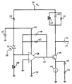
- Fig. 1 is a schematic diagram of a circuit constructed in accordance with the present invention.
- Fig. 1 an input infrared light beam 120, having a carrier which has been modulated with information to be detected, is caused to impinge on a photodiode 101.
- photodiode 101 is shown as a single diode, it can if desired be composed of a plurality of photodiodes connected in parallel in order to maximize the amount of photo current generated by the light beam and to accommodate the reception of light from various angles and distances.
- eight Siemens type BPW34FA photodiodes were connected in parallel, yielding a total light receiving area of 0.56 cm and an operating capacitance of about 170 pf. with the back-bias potential provided.
- Optical filters that pass infrared (IR) and attenuate visible light are built in to the BPW34FA photodiodes that were used. This tends to ameliorate the problem of lower frequency optical interference from fluorescent lights.
- the Q of the tank circuit may have to be lowered in order to broaden the bandwidth of the input circuit. If one attempts to achieve this by simply connecting a resistor directly in parallel with the tank circuit, the reduction in signal to noise ratio (arising from the resistor Johnson noise) may be unacceptable.
- the biasing voltage for photodiode 101 is supplied from a positive potential source 104, V s , through a resistor 102 to the cathode of photodiode 101.
- a capacitor 103 is connected between the cathode of the photodiode and ground potential to provide a low-pass filtering action with resistor 104 which attenuates any unwanted noise components that may be present on power supply terminal 104.
- the anode of photodiode 101 is connected through inductor 105 to ground potential. Since capacitor 103 provides a low impedance at the carrier frequency, photodiode 101 and inductor 105 are essentially connected in parallel to form a parallel resonant circuit at the carrier frequency.
- the signal at the carrier frequency, bearing the modulated data of interest, is coupled from the junction of photodiode 101 and inductor 105 to the input of an inverting amplifier 108.
- the power input to amplifier 108 is connected by way of line 118 to receive the filtered potential available at the cathode of photodiode 101, and line 119 completes the power connection to ground for amplifier 108.
- the output of amplifier 108 on line 117 is connected both to one terminal of a feedback capacitor 106 and to one terminal of a feedback resistor 107.
- the other terminals of capacitor 106 and resistor 107 are connected to the inverting input of amplifier 108 to form a negative feedback arrangement.
- amplifier 108 was implemented with an inverted cascode amplifier having a gain of 40 by using a Motorola MPSA18 NPN transistor input stage.
- This amplifier exhibited an input series noise spectral density of 3.5 nV/(Hz.) 1/2 and negligible phase shift at the operating frequency of 1 MHz.
- capacitor 106 and resistor 107 respectively, cause the generation of an input impedance having capacitive and resistive components across a resonant tank circuit including photodiode 101 and inductor 105.
- the capacitive component influences the resonant frequency of the tank circuit, and inductor 105 is preferably an adjustable inductor which can be changed to provide the correct tank resonant frequency.
- the resistive component of the amplifier effective input impedance advantageously reduces the Q in a manner to be described herein after.
- the depletion layer thickness is essentially proportional to the square root of the total reverse bias voltage V b .
- the photodiode capacitance C d is proportional to the reciprocal of the battery voltage: C d ⁇ 1 V b
- the capacitive component of the input impedance is equal to (G+1) times the feedback capacitor C f .
- Feedback resistor 107 provides a resistive component to the input impedance of amplifier 108 which in turn provides this damping, and it does so in a way that does not result in the introduction of as large an amount of Johnson noise as would be the case if the tank circuit were simply damped by a parallel resistor.
- the receiver Since the input tank bandwidth is quite large in the embodiment which was constructed, the receiver still had a significant gain at lower frequencies where large quantities of modulating interfering signals can still exist. Accordingly, the output of amplifier 108 is connected by way of line 117 to the base of a common emitter stage using NPN transistor 109. This stage of amplification using transistor 109 has two additional methods of interference filtering.
- the base of transistor 109 is connected to a constant current sink 110 to bias the transistor. Also connected from the emitter of transistor 109 to ground potential is a series circuit consisting of capacitor 111 and resistor 220.
- capacitor 111 is chosen such that it presents a significant impedance at low frequencies but is insignificant relative to the value of resistor 220 at the carrier frequency. Accordingly, the gain provided by transistor 109 at frequencies lower than the carrier frequency is considerably reduced.
- the collector of transistor 109 is connected to a parallel resonant circuit consisting of inductor 114 and capacitor 115, the other end of which is connected to the positive potential source 104.
- This parallel resonant circuit is chosen to resonate at the carrier frequency and is damped by the action of resistor 116 which is connected in parallel with the resonant circuit in order to maintain the proper bandwidth.
- a capacitor 113 couples the signal at the carrier frequency to an output terminal which can be connected to further stages of amplification, followed by appropriate demodulation, using standard techniques that are well known in the radio receiver and data communications arts.
- the resonant, capacity cancelling, actively damped IR receiver approach that is described herein is advantageously compatible with all three of the standard modulation techniques, namely frequency shift keying (FSK), phase shift keying (PSK), and amplitude shift keying (ASK).
- FSK frequency shift keying
- PSK phase shift keying
- ASK amplitude shift keying
- the receiver of Figure 1 can be used to drive a standard low-cost FM radio receiver chip such as the Motorola MC3359.
- This chip incorporates a standard quadrature demodulator which can be used to recover the signal information.
- An even better approach is to use the demodulator described in my copending patent application entitled, "Phase Locked Quadrature Demodulator".
- an inverting amplifier configuration other than the cascode can be used to provide compensation for the change in capacitance of the photodiode.
Landscapes
- Physics & Mathematics (AREA)
- Electromagnetism (AREA)
- Engineering & Computer Science (AREA)
- Computer Networks & Wireless Communication (AREA)
- Signal Processing (AREA)
- Amplifiers (AREA)
- Optical Communication System (AREA)
Applications Claiming Priority (2)
| Application Number | Priority Date | Filing Date | Title |
|---|---|---|---|
| US08/316,587 US5481104A (en) | 1994-09-30 | 1994-09-30 | Photodetector circuit with actively damped tuned input |
| US316587 | 1994-09-30 |
Publications (1)
| Publication Number | Publication Date |
|---|---|
| EP0704994A1 true EP0704994A1 (fr) | 1996-04-03 |
Family
ID=23229681
Family Applications (1)
| Application Number | Title | Priority Date | Filing Date |
|---|---|---|---|
| EP95306639A Withdrawn EP0704994A1 (fr) | 1994-09-30 | 1995-09-20 | Circuit photodétecteur avec entrée accordé à amortissement actif |
Country Status (6)
| Country | Link |
|---|---|
| US (1) | US5481104A (fr) |
| EP (1) | EP0704994A1 (fr) |
| JP (1) | JPH08125454A (fr) |
| KR (1) | KR960012797A (fr) |
| CN (1) | CN1126910A (fr) |
| CA (1) | CA2156338A1 (fr) |
Cited By (2)
| Publication number | Priority date | Publication date | Assignee | Title |
|---|---|---|---|---|
| EP0766889B1 (fr) * | 1995-04-21 | 2003-12-10 | Koninklijke Philips Electronics N.V. | Recepteur optique, syntoniseur et reseau optique |
| KR20040050948A (ko) * | 2002-12-11 | 2004-06-18 | 한국전자통신연구원 | 유도성으로 보상된 고속 광전 모듈 |
Families Citing this family (21)
| Publication number | Priority date | Publication date | Assignee | Title |
|---|---|---|---|---|
| US5763873A (en) * | 1996-08-28 | 1998-06-09 | Patchen, Inc. | Photodetector circuit for an electronic sprayer |
| US6307659B1 (en) | 1997-09-24 | 2001-10-23 | Stratos Lightwave, Inc. | Optoelectronic transceiver having an adaptable logic level signal detect output |
| US6046445A (en) * | 1998-04-15 | 2000-04-04 | Spectra Precision, Inc. | Solar powered laser receiver circuit |
| US7155133B2 (en) * | 2002-02-12 | 2006-12-26 | Finisar Corporation | Avalanche photodiode controller circuit for fiber optics transceiver |
| US7002131B1 (en) | 2003-01-24 | 2006-02-21 | Jds Uniphase Corporation | Methods, systems and apparatus for measuring average received optical power |
| US7215883B1 (en) | 2003-01-24 | 2007-05-08 | Jds Uniphase Corporation | Methods for determining the performance, status, and advanced failure of optical communication channels |
| JP2006303668A (ja) * | 2005-04-18 | 2006-11-02 | Matsushita Electric Ind Co Ltd | 出力インピーダンス可変回路 |
| CN100560161C (zh) * | 2006-02-17 | 2009-11-18 | 杭州大力神医疗器械有限公司 | 光电指脉传感红外线发生装置 |
| FR2940432B1 (fr) * | 2008-12-23 | 2011-01-21 | H2I Technologies | Dispositif pour quantifier et localiser un signal lumineux module a une frequence predeterminee |
| US20110169520A1 (en) * | 2010-01-14 | 2011-07-14 | Mks Instruments, Inc. | Apparatus for measuring minority carrier lifetime and method for using the same |
| US8901997B2 (en) * | 2011-11-16 | 2014-12-02 | The Brain Window, Inc. | Low noise photo-parametric solid state amplifier |
| US9800350B2 (en) * | 2012-01-23 | 2017-10-24 | Intel Corporation | Increased density SFP connector |
| CN102832898B (zh) * | 2012-09-24 | 2015-03-18 | 北京新雷能科技股份有限公司 | 一种滤波器阻抗补偿装置及一种滤波器 |
| US11428790B2 (en) * | 2017-06-05 | 2022-08-30 | Texas Instruments Incorporated | Narrowband TIA and signaling for optical distance measurement systems |
| US11444581B2 (en) * | 2018-03-15 | 2022-09-13 | Mitsubishi Electric Corporation | Integrated circuit and light receiver |
| US11050962B2 (en) | 2018-07-20 | 2021-06-29 | Raytheon Company | Dual mode focal plane array having DI and BDI modes |
| US10917599B2 (en) * | 2018-07-20 | 2021-02-09 | Raytheon Company | Focal plane array having ratioed capacitors |
| CN111953305A (zh) * | 2019-05-17 | 2020-11-17 | 中国科学院物理研究所 | 一种前置交流放大器及其应用 |
| DE102019212225A1 (de) * | 2019-08-14 | 2021-02-18 | Fraunhofer-Gesellschaft zur Förderung der angewandten Forschung e.V. | Treiberschaltung für ein oder mehrere optische Senderbauteile, Empfängerschaltung für ein oder mehrere optische Empfangsbauteile zur optischen drahtlosen Kommunikation und Verfahren |
| US10917093B1 (en) * | 2019-11-05 | 2021-02-09 | Micron Technology, Inc. | Self-adaptive termination impedance circuit |
| CN118132889B (zh) * | 2024-01-04 | 2025-02-18 | 中科院广州电子技术有限公司 | 一种电容耐压绝缘测试阈值自动获取方法 |
Citations (2)
| Publication number | Priority date | Publication date | Assignee | Title |
|---|---|---|---|---|
| JPS63303503A (ja) * | 1987-06-04 | 1988-12-12 | Omron Tateisi Electronics Co | 光受信回路 |
| JPH05218806A (ja) * | 1992-01-31 | 1993-08-27 | Nec Corp | 光受信回路 |
Family Cites Families (7)
| Publication number | Priority date | Publication date | Assignee | Title |
|---|---|---|---|---|
| JPS5533324A (en) * | 1978-08-30 | 1980-03-08 | Hitachi Ltd | Remote control receiver |
| US4751745A (en) * | 1986-10-17 | 1988-06-14 | Rockwell International Corporation | High frequency signal filter apparatus |
| IL84684A (en) * | 1986-12-31 | 1992-09-06 | Hughes Aircraft Co | Electronically tuneable fiber-optic receiver for narrow band microwave signal reception |
| US5142401A (en) * | 1990-06-28 | 1992-08-25 | Raynet Corporation | Apparatus and method for a linear, wideband sensitive optical receiver |
| US5373152A (en) * | 1992-01-31 | 1994-12-13 | Nec Corporation | Resonance-type optical receiver circuit having a maximum amplifier input controlled by using an amplifier feedback and its method of receiving |
| JP3207240B2 (ja) * | 1992-04-10 | 2001-09-10 | キヤノン株式会社 | フォトダイオードのバイアス回路 |
| US5296697A (en) * | 1992-08-10 | 1994-03-22 | Parkervision, Inc. | Detection circuit for maintaining constant signal transfer characteristics of a light-sensitive detector |
-
1994
- 1994-09-30 US US08/316,587 patent/US5481104A/en not_active Expired - Lifetime
-
1995
- 1995-08-17 CA CA002156338A patent/CA2156338A1/fr not_active Abandoned
- 1995-09-20 EP EP95306639A patent/EP0704994A1/fr not_active Withdrawn
- 1995-09-27 CN CN95117391A patent/CN1126910A/zh active Pending
- 1995-09-29 KR KR1019950034031A patent/KR960012797A/ko not_active Withdrawn
- 1995-09-29 JP JP7275116A patent/JPH08125454A/ja active Pending
Patent Citations (2)
| Publication number | Priority date | Publication date | Assignee | Title |
|---|---|---|---|---|
| JPS63303503A (ja) * | 1987-06-04 | 1988-12-12 | Omron Tateisi Electronics Co | 光受信回路 |
| JPH05218806A (ja) * | 1992-01-31 | 1993-08-27 | Nec Corp | 光受信回路 |
Non-Patent Citations (3)
| Title |
|---|
| PATENT ABSTRACTS OF JAPAN vol. 13, no. 142 (E - 739) * |
| PATENT ABSTRACTS OF JAPAN vol. 17, no. 661 (E - 1471) * |
| TAKACHIO ET AL: "A novel resonance-type optical receiver for high-speed optical heterodyne transmission systems", JOURNAL OF LIGHTWAVE TECHNOLOGY, vol. 7, no. 9, NEW YORK US, pages 1371 - 1378, XP000065618, DOI: doi:10.1109/50.50716 * |
Cited By (2)
| Publication number | Priority date | Publication date | Assignee | Title |
|---|---|---|---|---|
| EP0766889B1 (fr) * | 1995-04-21 | 2003-12-10 | Koninklijke Philips Electronics N.V. | Recepteur optique, syntoniseur et reseau optique |
| KR20040050948A (ko) * | 2002-12-11 | 2004-06-18 | 한국전자통신연구원 | 유도성으로 보상된 고속 광전 모듈 |
Also Published As
| Publication number | Publication date |
|---|---|
| JPH08125454A (ja) | 1996-05-17 |
| KR960012797A (ko) | 1996-04-20 |
| CN1126910A (zh) | 1996-07-17 |
| CA2156338A1 (fr) | 1996-03-31 |
| US5481104A (en) | 1996-01-02 |
Similar Documents
| Publication | Publication Date | Title |
|---|---|---|
| US5481104A (en) | Photodetector circuit with actively damped tuned input | |
| US7069062B2 (en) | Transceiver capable of causing series resonance with parasitic capacitance | |
| US6885184B1 (en) | Galvanically isolated voltage sensing circuit | |
| EP0660504B1 (fr) | Circuit oscillateur | |
| KR920007091B1 (ko) | 신호강도 표시기 | |
| KR100574753B1 (ko) | 전자 기기를 위한 웨이크업 회로 | |
| US4513209A (en) | Level detector | |
| US5031196A (en) | Receiver for use in a remote control system | |
| US4255812A (en) | Signal regenerating apparatus with DC compensation | |
| US4359693A (en) | Full wave amplitude modulation detector circuit | |
| US5459434A (en) | Detector amplifier for standby system | |
| US4264867A (en) | Demodulator circuit for frequency-modulated signal | |
| US3931576A (en) | Automatic gain control circuit for radio receiver | |
| US3852686A (en) | Automatic frequency control circuit | |
| US4319195A (en) | Demodulator for amplitude modulated signal having high input impedance | |
| US4218776A (en) | Parametric optical detector | |
| US4027268A (en) | Demodulator for PM or FM signals | |
| US5629959A (en) | Wideband square-law detector having a triangular frequency characteristic as well as a transmission system and a receiver including such a detector | |
| JPS596014Y2 (ja) | Am受信機の同調信号発生回路 | |
| JPS5920299B2 (ja) | 光電変換回路 | |
| JPH05218806A (ja) | 光受信回路 | |
| KR830000137B1 (ko) | Fm 검파기 | |
| SU674195A1 (ru) | Частотный детектор | |
| JPS6149846B2 (fr) | ||
| RU1771062C (ru) | Частотный детектор на расстроенных контурах |
Legal Events
| Date | Code | Title | Description |
|---|---|---|---|
| PUAI | Public reference made under article 153(3) epc to a published international application that has entered the european phase |
Free format text: ORIGINAL CODE: 0009012 |
|
| AK | Designated contracting states |
Kind code of ref document: A1 Designated state(s): DE ES FR GB IT |
|
| 17P | Request for examination filed |
Effective date: 19960918 |
|
| STAA | Information on the status of an ep patent application or granted ep patent |
Free format text: STATUS: THE APPLICATION HAS BEEN WITHDRAWN |
|
| 18W | Application withdrawn |
Withdrawal date: 19971024 |